Close
0%
0%

DrDAC USB Audio DAC

An escape from the tyranny of low-quality soundcards

Similar projects worth following
Most laptops, desktops, and phones come with low-quality soundcards built-in, and most users never get to experience the wonder of high-quality audio coming from their device. This project is an effort to restore the wonder and details that high-quality sound contains by making a high quality sound card available in a DIY package to everyone, at a price roughly equivalent to a new pair of mid-end earbuds.

This project is an extension of the pupDAC project by cobaltmute, and was started for a school project.

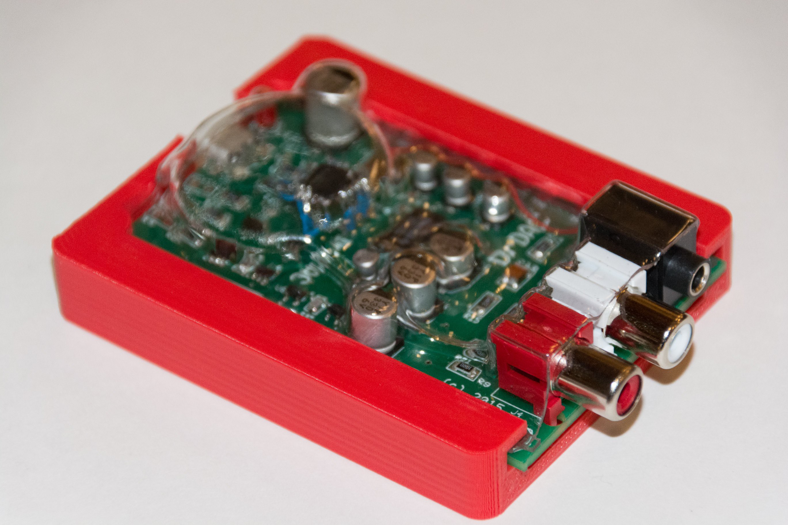
High quality sound should be a right, not a luxury. To that end, I worked to make a cheaper, open-source version of cobaltmute's pupDAC for a EE PCB design class.

Over the course of a semester, we selected a circuit, analyzed it, turned it into a MultiSim schematic, turned that schematic into a board layout , and then ordered and built the board. I knew that it would be a challenge to build this board, as I was targeting a very small footprint (2"x3" for 80 components) and a relatively complicated design, especially for my first board layout ever.

Soldering Challenges

The following video shows a timelapse of me constructing the board, which required great soldering dexterity.

For my board, I started with a solder paste mask, and spread solder paste over the top surface (0:01). Then I used tweezers to place the parts, and stuck it into a reflow oven. Here, I discovered that our school's default temperature profile was inadequate for my board, because it essentially flash-flowed the oven. It didn't have a soak time, which meant that the ground plane didn't have enough time to heat up, and any parts connected to the ground plane (like all my capacitors) needed manual soldering to melt the paste.

Even with this complication, It would've been a simple job, except that I ran into a nasty problem after I had already started assembling the board: the main IC, a USB to I2S audio data converter, was too large for the footprint (I later traced the error to MultiSim having a too-small footprint for the TQFP-32 package).

So, like any enterprising student whose grade relies on his circuit working, I decided to take the logical next step: solder jumper wires directly from the pads to the leads of the IC (no, I couldn't have ordered a new board, I only had a week till the semester ended, and I still had to redesign the board).

Even though both my professor and our lab technician recommended against this jumper idea, I decided to carry on with my audacious plan. I initially thought I could find some 8-wide ribbon cable, and solder that to the pads, and then fan that out to the IC itself. However, the insulation was too wide, and I couldn't get the leads to stay well-joined to the pads. At this point, I should probably note that the leads of a TQFP-32 are spaced .8mm apart, and the pad that I was soldering onto was spaced at .5mm apart. The next step was to get some wire wrap from the school's technician, which was between 30-32 gauge, and JUST BARELY fit onto the pads (I believe they are 10 mil pads).

I couldn't find wire strippers that worked for wire that small, and using my teeth was ineffective (I ended up bending the wire more than stripping it). So I figured out a way of stripping the wire that was more effective than any other method I found yet, with a yield of maybe 50%... I used a knife to cut the wire to length (roughly 1/4"). Then I would roll the wire under the blade while applying very light pressure. Half of the time, this would create enough of an edge for me to pull the insulation off with a fingernail (the other half it would just cut straight through the wire, and I'd start over). This can be seen at 1:08 in the video.

After making the 32 jumpers needed to connect the IC to the pads (and a few extras for the inevitable problems. And then a few more...), I got down to the slow and touchy process of actually soldering them to the pads (0:47). After getting them onto the pads (1:17, a process that wasn't totally included in the video), I then had to somehow carefully bend the fragile fragile wires up (without breaking them or tearing them off the board), and then solder the IC onto them without heating them too much that the pad end of the wire would come loose. Which happened more times than I would care to admit...

Once I found a rhythm, it was fairly easy to get going, but I still ran into some problems. One was the above-mentioned wires coming loose. If the wire was on the end of a set of 8, it was no problem. I'd just put a new one...

Read more »

  • 1 × PCM2706 USB Audio DAC (I2S Data out)
  • 1 × OPA2836 Amplifier and Linear ICs / Operational Amplifiers
  • 1 × PCM1794 I2S to Balanced Audio. Data Converters / Digital to Analog Converters (DACs)
  • 1 × MCP100T-315I/TT IC Supervisor. Power Management ICs / Power Supply Support
  • 2 × TPS79333 3.3V LDO Regulator. Power Management ICs / Linear Voltage Regulators and LDOs

View all 10 components

  • Board Revision Planning

    drewrisinger06/30/2015 at 02:22 0 comments

    So I'm currently trying to decide what to do next with this project. I have a few other projects floating around that have taken priority (such as collaborating with someone who's building something based on my ESP-01/03 Breakout), and work and travel have gotten in the way recently.

    My current thought is to fork my effort, and create two simultaneous layouts with different timeframes:

    • Minor revision: only change the footprint of the blasted PCM2706 that gave me such soldering adventures last time. This will be an easy fix, but I run the risk of the board still not working because I haven't isolated the problem.
    • Major revision: complete redesign. Reexamine all the circuit components, layout, and logic, to confirm that everything is wired right, and that there are no better parts for the job that could reduce my circuit complexity.
      • For example, a high quality USB DAC chip that could output great signal straight from the chip itself (would replace both PCM2706 & PCM1794).

    However, forking will greatly increase cost, as each current run of boards will cost $30 at OSH Park (2"x3" board = $5*(2*3)=$30 for 3), and the parts in the BOM costs roughly $60 each, running to $90 for each iteration of the board (assuming I don't retrieve parts off the outdated boards, which is hard without a hot air gun).

    The better solution would be to order a set of parts that I think I will use, and a bunch of SMD to breadboard breakouts, and try to wire everything up in a breadboard to confirm that it will actually work before I layout & order the board. This has the advantage of enabling troubleshooting & reconfiguring of the circuit, but at the expense of complexity, a large breadboard needed, and

    My least favorite option, but maybe the best to fit within my life, is to simplify the board, and just use the first-stage PCM2706 into the opamp. This would prove that the opamp and PCM2706 are working, and have a higher chance of success. It would also be simpler, which will allow me a quicker turnaround time and to fit it between my other projects.

    If anyone has any opinions, please let me know! I'm currently leaning towards cutting features and getting the PCM2706/opamp combo working on a smaller board, and then trying to get the PCM1794 added in after that's working.

  • Schematic v1.0

    drewrisinger05/28/2015 at 05:44 0 comments

    This is the schematic that corresponds to version 1.0 of my design. It's divided into 4 sections: the USB section (which takes USB signals in, and outputs I2S Data), the I2S DAC (which outputs a balanced audio signal), the output opamp power supply section, and the opamp circuit itself, which provides the output.

    Read more »

  • Constructing the Case

    drewrisinger05/28/2015 at 05:25 0 comments

    I was really fortunate to have access to my school's manufacturing equipment in constructing my case, even though I'm an Electrical Engineering major.

    I was able to construct a case in two parts, with some assistance on the CAD side.

    Read more »

  • Coming Soon:

    drewrisinger05/28/2015 at 05:08 0 comments

    This here is version 1.0 of my circuit board & layout. I'm hoping to add in some posts on the design of the circuit, as well as future revisions as I work towards a 2.0 version that addresses the many problems I had with this board (such as it not outputting audio, which is only a minor problem ;)

View all 4 project logs

Enjoy this project?

Share

Discussions

macsimski wrote 07/17/2016 at 10:44 point

I use regular 0,2 mm enamelled copper wire for patches on boards. if you heat up the bare end of the wire and add some solder, the enamel will just burn away.  My methode would be to make a amount of wires all the same length and tin the ends. then solder the wires flat onto the pcb and bend them in a curve back up. A very sharp tweaser is a must. I can dot his with a regular weller wtcp with the sharpest point available. Oh and tinning the pins of the tqfp beforehand also helps.

  Are you sure? yes | no

John August wrote 06/11/2015 at 06:40 point

Very cool! Check out that jumper wire work!! You should have a look at my project. I wanted to incorporate a DAC into my design but essentially ran out of time and board real-estate! Is this class you have taken an Undergrad course? I've been wishing my school offered such a class. My work was done independently in a senior design class with no such instructor guidance. Also, WOW, I just watched your time lapse. You did that all by hand! Unbelievable, I commend you on your patience. Our group used the Aoyue 968A which can be had on amazon for a very reasonable price considering what you get. It is a TOP notch hot air station and you should totally buy it. It will save you so much time and the results are that much more professional. We primarily used 0603 package but for my next iteration I want to push it down to 0402 which is SUPER tiny. This will let me shrink things down just that much more. Skulls to you!

  Are you sure? yes | no

Michele Perla wrote 06/04/2015 at 09:00 point

Dude, that PCM1794 has out-of-this-world specs, good choice! 

Anyway, I don't think that the PCM2706 is a good pairing for that DAC, 98 dB SNR vs 130ish :D btw, neat project!

  Are you sure? yes | no

drewrisinger wrote 06/10/2015 at 02:56 point

Michele, interesting comment. My understanding is that the SNR of the PCM2706 doesn't actually matter. Essentially, the PCM2706 acts as a digital interface to the PCM1794. So it will take the USB signal from the computer, and convert it to the digital I2S protocol (I don't remember what the bit-depth for the PCM2706 is off top of my head, but I think it's 16-bit...). For this digital portion of the circuit, SNR shouldn't matter, as long as the I2S signals quickly transition 0->1. Noise shouldn't significantly affect this transition from 0-> 3.3V, because the noise would have to be more than about 1.7 V to trigger a high value in typical transistor logic.


Then the PCM1794 is what actually provides the analog output. This is really where you want the noise floor to be low (high SNR), because this is what is output straight to the opamp and then to the headphones. A low SNR here would probably cause noticeable white noise in the background. The 96 dB SNR of the PCM2706 doesn't actually matter, because it's not output to anything except another digital chip.


I agree, they're not terribly well-matched (I used the pupDAC as a basic parts list for this, and changed a few things), and I might try to find a better match in a future redesign. But I'll still probably keep the PCM1794, cause there's no kill like overkill. And it's super easy to not make that the weak link in my design.


From what I understand, the PCM1794 is typically used in professional digital mixing boards (such as concert audio engineers or recording studios) might have, which kind of explains the high price and fantastic specs.

  Are you sure? yes | no

Similar Projects

Does this project spark your interest?

Become a member to follow this project and never miss any updates