Hayden Kroepfl
-
Now it's own board
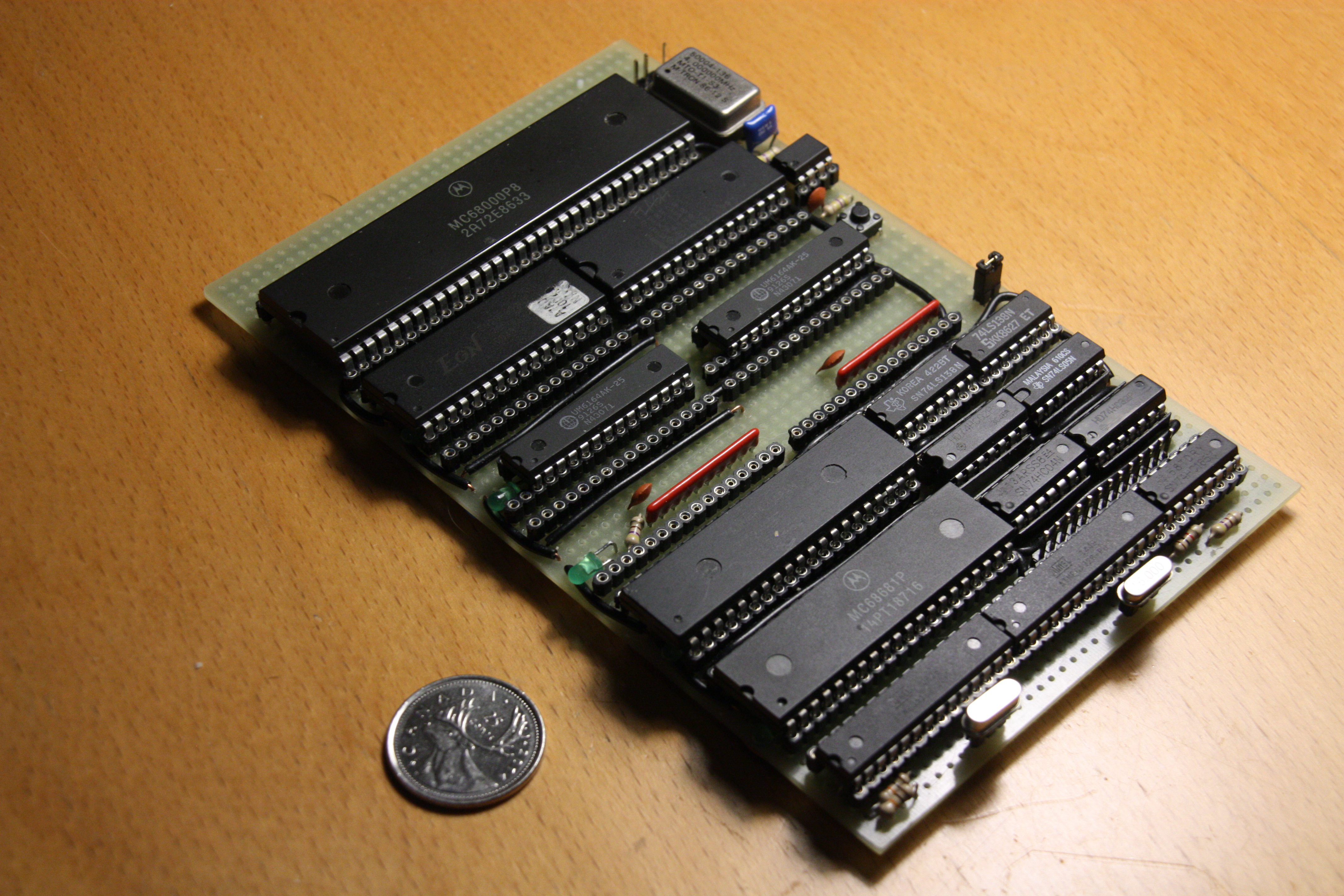
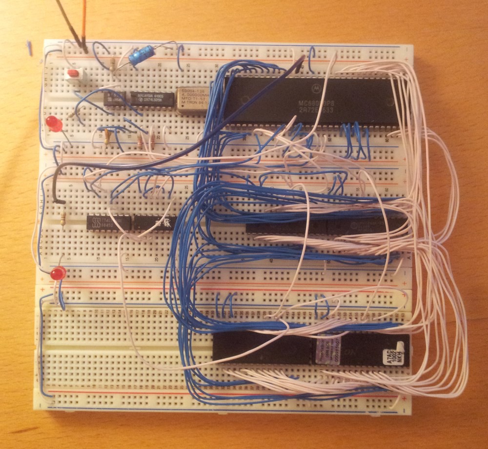
07/19/2016 at 00:31 • 0 comments![]() Well the breadboard part of my computer is no longer there. It's been all moved onto a single 3U euro-card sized protoboard. So I guess now I've got to change the title of the project. Was quite a bit of work to wire up the hundreds of point to point connections. All of it was done using 30AWG wire wrap wire, soldered point to point.
Well the breadboard part of my computer is no longer there. It's been all moved onto a single 3U euro-card sized protoboard. So I guess now I've got to change the title of the project. Was quite a bit of work to wire up the hundreds of point to point connections. All of it was done using 30AWG wire wrap wire, soldered point to point. ![]()
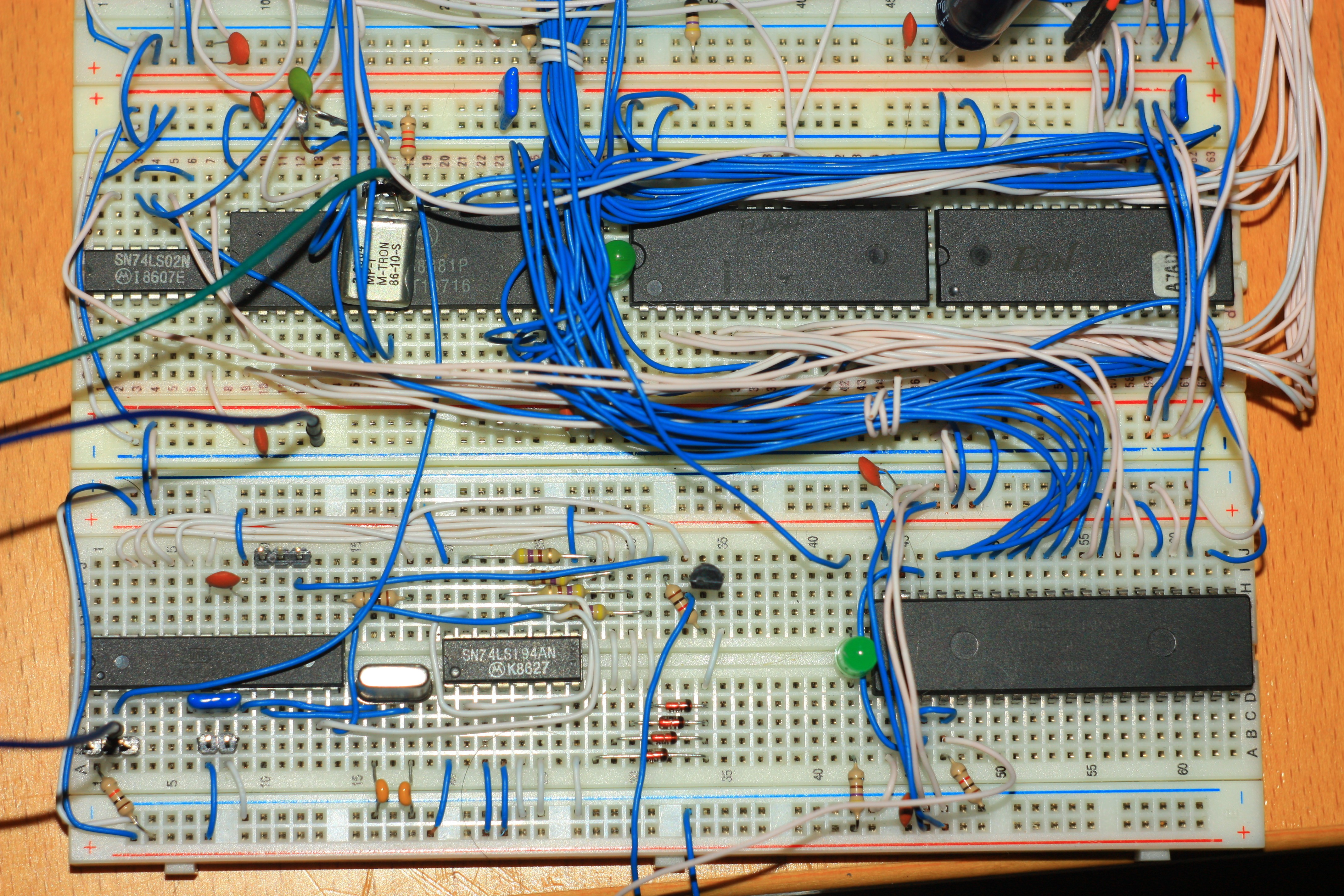
I changed a few things with the circuit when I moved it over. The main change is in how the address bus is decoded. I opted to go a bit excessive and used two 74138s to fully decode the entire 16MB space. Each output corresponds to a 1MB section of address space. ROM and peripherals are mapped into the lower 8MB, and RAM is mapped in the upper. On the board you can see two unused sockets, with the upper one having a RAM chip connected to part of it. The board is designed to take 2MB of memory in the form of 4 AS6C4008 4Mbit SRAMs, I just haven't ordered them yet. So for compatibility I added a inner header on the first RAM socket, so that I could put my 6164 SRAM chips in in the mean time.
One thing I should have done was to eliminate the 7404 hex inverter since I'm only using one gate of it, and I've got two NOR gates still unused.
![]()
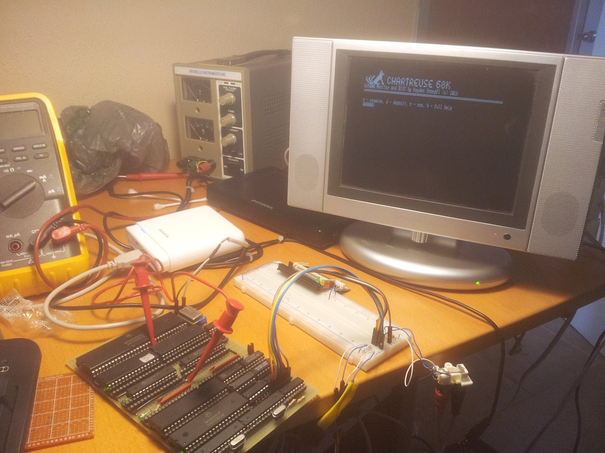
Also added/changed was the video interface. I chose to replace my 32x24 column color text display with Grant Searle's 80x25 B/W display for AVRs. Along with the corresponding PS/2 keyboard and serial driver interface. On the board this can be seen at the very bottom with an ATMEGA168 on the left handling PS/2 and serial, an ATMEGA328 in the middle generating the video, and a 74HC165 at the right shifting out the video bits. One thing I'm thinking of doing is changing the interface AVR to instead scan a keyboard matrix taken from a laptop. This would allow me to more easily find a keyboard that would fit in my goal of making this computer into a laptop.
To go along with these changes I've updated the original monitor program on my GitHub to use the new memory map and display.
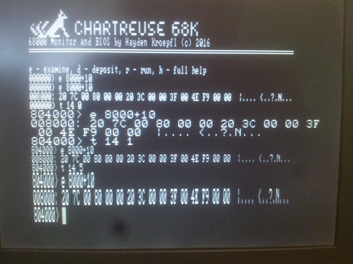
I've also partly re-wrote the monitor such that it can function as a BIOS for my operating system that I am currently written. I've added a number of BIOS routines accessible using trap #15 including standard screen writing, serial port access, a simple beep from the YM2149, and disk access routines. The new monitor/BIOS can also be found on my GitHub.
I still don't have any storage medium hooked up. I'd like to do IDE since it's trivially simple to implement with the 68k's BUS. Only requiring some logic to generate the positive level write and read signals from the R/W and AS pins. The problem though is that I've got almost no board space left. I've got just enough space to put an expansion header, or to put the IDE interface. What I really should have done was to put the video generator onto it's own board as it only requires 4 wires (Vcc, GND, Rx, Tx) to interface with the computer, while IDE would take something around 30.
There's also a slight hardware bug, due to one of my ROMs being a boot block ROM. One of the pins that's normally an unused or an address line pin is instead an active low chip disable. Since I wired the board such that I could replace my random pulled ROMs with new 4Mbit ROMs that pin was being pulled low by an address line. As a temporary fix till I get my ROMs in, I've bent the pin out of the socket. And used a clip to pull that pin to Vcc as unfortunately it can't just be left floating.
![]()
-
Video, Audio, Progress!
05/12/2016 at 03:22 • 0 commentsAlright so it's been quite a while since I posted an update. Most of the work done on this update was done a few months ago, but school got in the way of getting it polished up a bit and written up. So, things that have been done since my last update. First things is that I've added a custom color NTSC serial terminal based on a ATMEGA328.
![]()
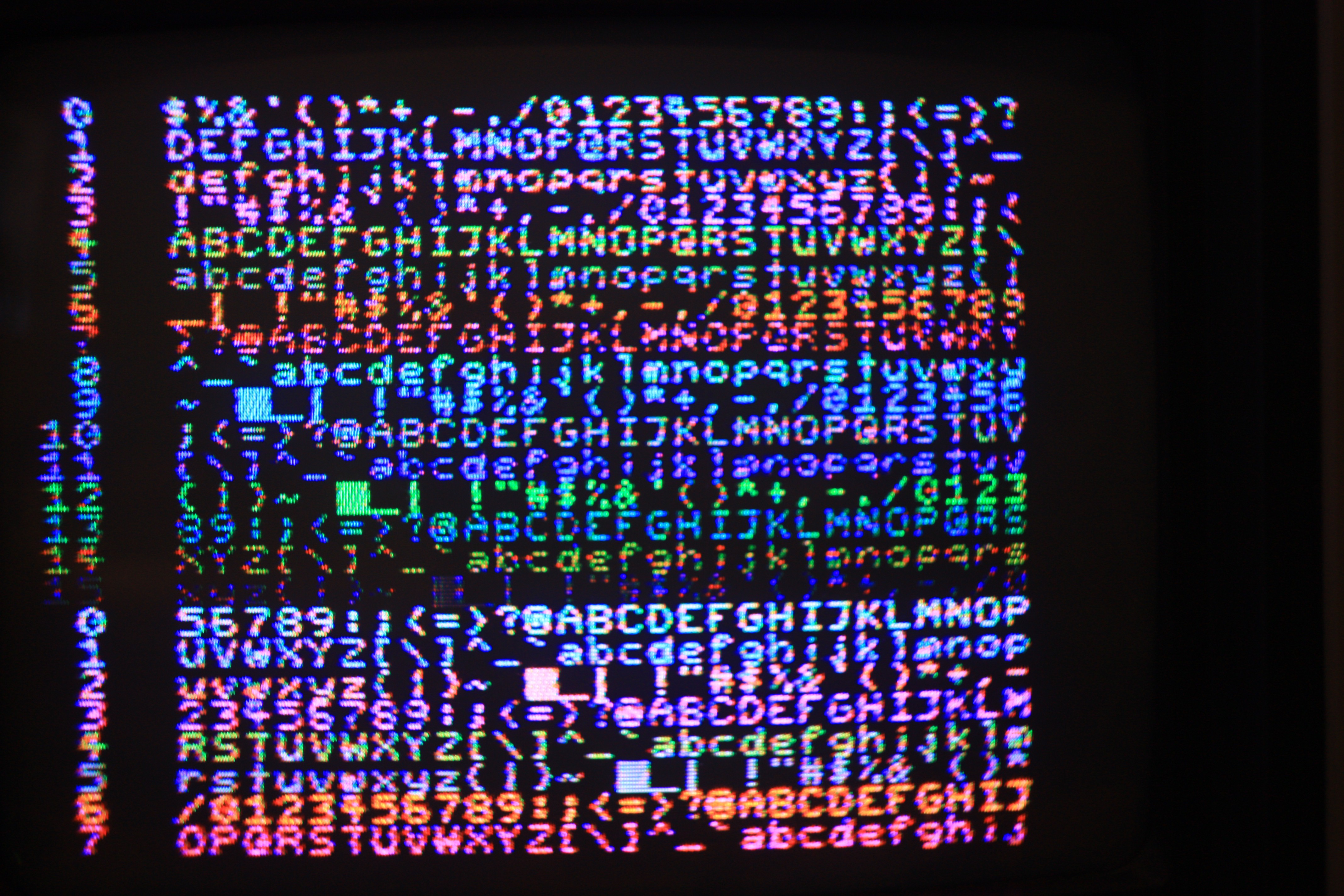
The video terminal is based on an earlier project of mine which was a B/W 40 column terminal with PS/2 keyboard running on a stock Arduino Duemilanove. For this project I decided I wanted a color terminal, so I redesigned the project from scratch using a bare ATMEGA328, A 14.318MHz crystal (4x NTSC color burst), and a 4 bit shift register to generate different phases of 3.8MHz. The downside of moving to color with the lower clock frequency was that I was unable to squeeze out more than 32 columns of text properly (also not helped by the SPI hardware in the ATMEGAs putting out a 9th bit for every byte sent). To support color over the serial terminal I added a parser for ANSI escape sequences to the terminal, and assigned the various colors I got from the shift register to the ANSI colors.![]()
The second major addition was to add a YM2149F programable sound generator. I wanted my computer to be able to play chip-tunes of some sort, and the YM2149F used in the Atari ST seemded like a good candidate. The only downside to this chip was it's weird bus inheritied from the AY-3-8910, which I had to add an AND gate (7402) to my circuit to develop my minimal interface circuit. Since I wanted to use as little logic as possible, access the chip is a little odd. To select a register you write to $180000 with the register number, to write to the register you write the value to $180002, and if you want to read the value of the register you read from $180000. The chip also gives me access to 2 more 8-bit parallel ports if they are needed.
Finally the interrupt line was hooked up from the 68681 DUART to interrupt line one on the 68000. The proper way to do this would be to hook it up through a priority encoded, but since we're only dealing with one interrupt source we can simply hook it up to the low bit, and tie the others low. With the interrupt line we can now have an interrupt handler listen for new data recieved by the serial port, and put that into a ring buffer. Rather than having to poll for new data constantly. This also lets us recieve serial data when the program is busy doing other things. Another feature we can now use is the DUARTs built in timers and counters. For my computer I programed a 300Hz timer to serve as the main system tick as it was divideable by both 50Hz for the Atari ST music, and 60Hz for VSYNC. Though this may be too fast if I decide to write a multi-tasking operating system later since there's only around 13,000 cycles at 4MHz between interrupts.
To take advantage of these hardware upgrades the monitor program was updated to handle the interupts, as well as including a simple interrupt driven player for YM2149 chiptunes. I used the MYM format used by the Oric Software Development Kit (http://osdk.defence-force.org/index?page=documentation&subpage=ym2mym) as an alternative to the YM format for computers with limited memory. The YM format is optimized to be decompressed in full into memory, which would take around 250k for a standard song. The MYM is optimized to be decompressed in 128 length frames. My implementation of the decoder is far from optimal at decoding the format as there is a noticable pause every 2.5s as it refills the buffer. This is due to the decoder taking much longer than the 1/50th of a second that it has before the next register dump is needed. -
Update and Working Monitor Over Serial
08/31/2015 at 05:02 • 0 comments![]()
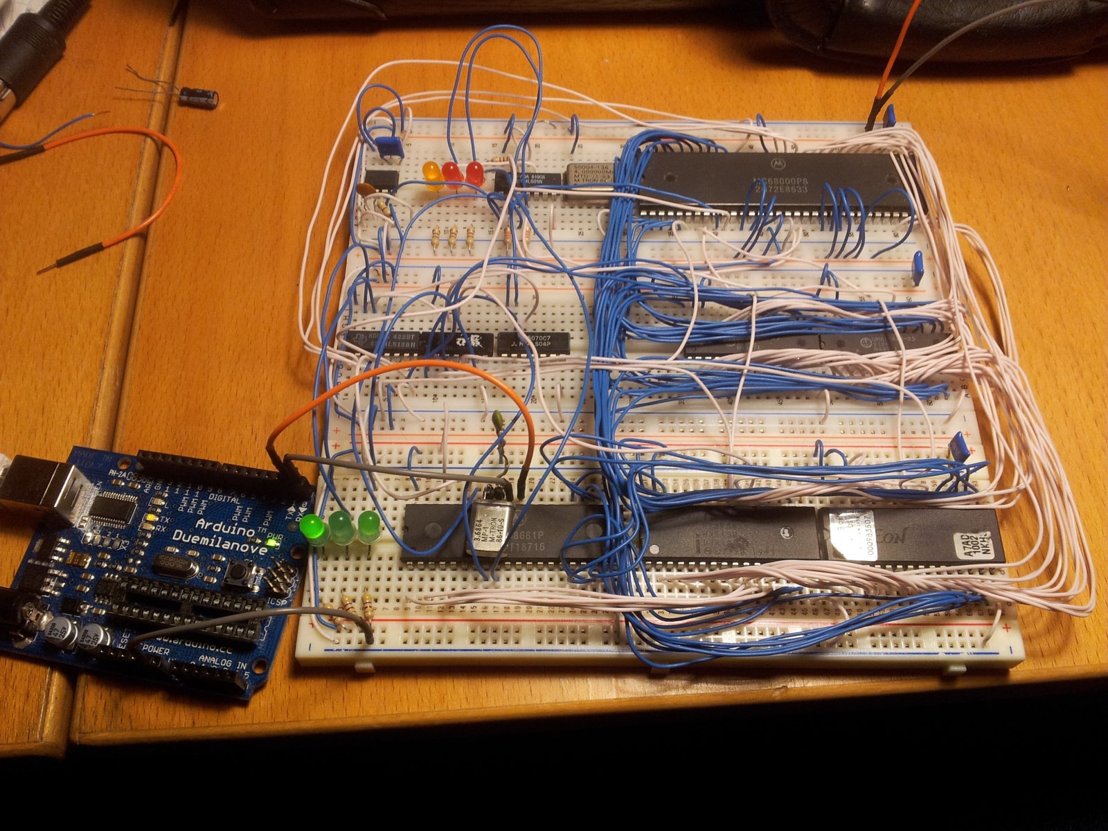
So a lot has changed since my last update on here, I've redone the address decoding to use a 74138 3-8 line decoder to allow me to partition the address space. I've added some status LEDs to help show the state the computer is sitting in, so I don't need to break out the logic probe as often. And the final, and probably the most important, addition is that I've added a 68681 Duart chip, giving me a means of input and output.
The 68681 chip wasn't a too difficult of a chip to add in, you just need to map it into the address space with it's chip select, attach it's 4 register select lines to the address bus, and tie it's 8 data lines onto one of the data buses. The other thing that adding it changed was necessitating me to add some /DTACK logic, rather than just grounding it, as the 68681 puts out a dtack signal. This was accomplished by using one of the open collector inverters to ground /DTACK when the 68681 isn't selected, but when it is selected it passes the /DTACK signal from the 68681 through a resistor to the 68000.
On the software side of things, my first tests were to get the 68681 to output something useful, for a while I wasn't succeeding and ended up putting the project on hold for a while. Fast forward to a couple weeks ago, I sat down to try and get it working again, and after writing the initialization code again (with the help of some online resources) I managed to get a Hello World! out of it. My computer was finally properly working.
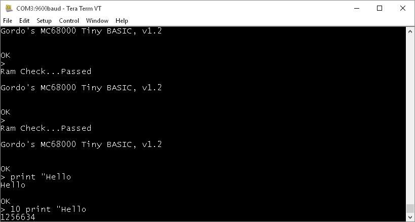
My next thought was to try and get a simple BASIC interpreter ported over to it, I quickly found a 68000 version of Tiny BASIC, which I modified the I/O to match my setup. As well as changing where it assumed RAM was. After quite a bit of debugging I finally got it to a partially working state as shown below.
![]()
I was able to get it to do get it to do a few things in interactive mode, namely the PRINT statement, but when I tried to store a program line, it would lock up. I tried doing some debugging over the serial port (hence the 1256634 on the last line) but what it was doing wasn't making much sense. In the end I was getting frustrated with it and moved on to writing my own program for the machine from scratch.
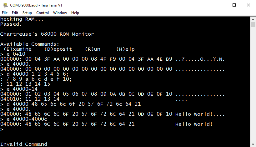
Enter my ROM Monitor. I decided I wanted to have a simple ROM Monitor program that would let me examine memory, deposit values into memory, as well as jump and execute to any address. I used this project as a way of getting some experience coding 68k assembly, as this computer is the first time I had done so. MarkeyJester's 68k Tutorial was a very nice reference for quickly learning the instructions I needed. Since I didn't want to spend all the time debugging over the serial port, flashing many ROMs and such I chose to use the built in simulator in Easy68k. What I did was write the I/O routines into functions that used the simulators I/O routines, so that when I was ready I'd swap in the routines I had written for the Tiny BASIC. After getting the monitor working as I wanted it in the simulator I finally flashed it to my ROM. Now it would have been great if it had worked perfectly first time, but there turned out to be a bug, when the examine function was told to examine more than 16 bytes at a time it would increment the address by 0x110 bytes instead, after a bunch of debugging I found the culprit, I was using only a byte of r4 (and so was using .b instructions), but I was doing a suba.l with it on an address, thus in the simulator where r4 was initialized to 0, it would work since the upper bytes were all 0, but on the real hardware where r4's initial state was unknown it failed. After fixing the code to initialize r4 and r3 in the dumpRAM routine, it worked perfectly on the real hardware.
![]()
Now as for what I'll be doing next, I'm not too sure. I may start with merging this and my arduino NTSC serial terminal project to give this computer a real computer feel. And having a TV output and keyboard would definitely do that. I also might give another try to porting a BASIC interpreter to it.
I posted my monitor over to my github if anyone feels like taking a look at it and/or using it. https://github.com/ChartreuseK/68k-Monitor
-
Blinken Lights
06/10/2015 at 22:04 • 0 comments -
It's Always The Thing You Never Think Of
06/10/2015 at 05:34 • 0 commentsWell now I'm feeling a little silly, the issue turned out to entirely be that I was flashing my Flash chips backwards. The tool I was using to output my byte code produces two bin files, name_0.bin and name_1.bin, for some reason I assumed that 0 would be the low bytes, and 1 the highs. However if you look in the program it does show that the even (low) bytes are in 1. Now with that sorted it worked! It finally worked! Though not before I had completely rewired the computer and added a proper reset circuit (based off this document the only changes made were that I used 470k resistors as I didn't have 1Meg handy, this gives a reset of 270ms which is still enough) .
The new computer:
![]()
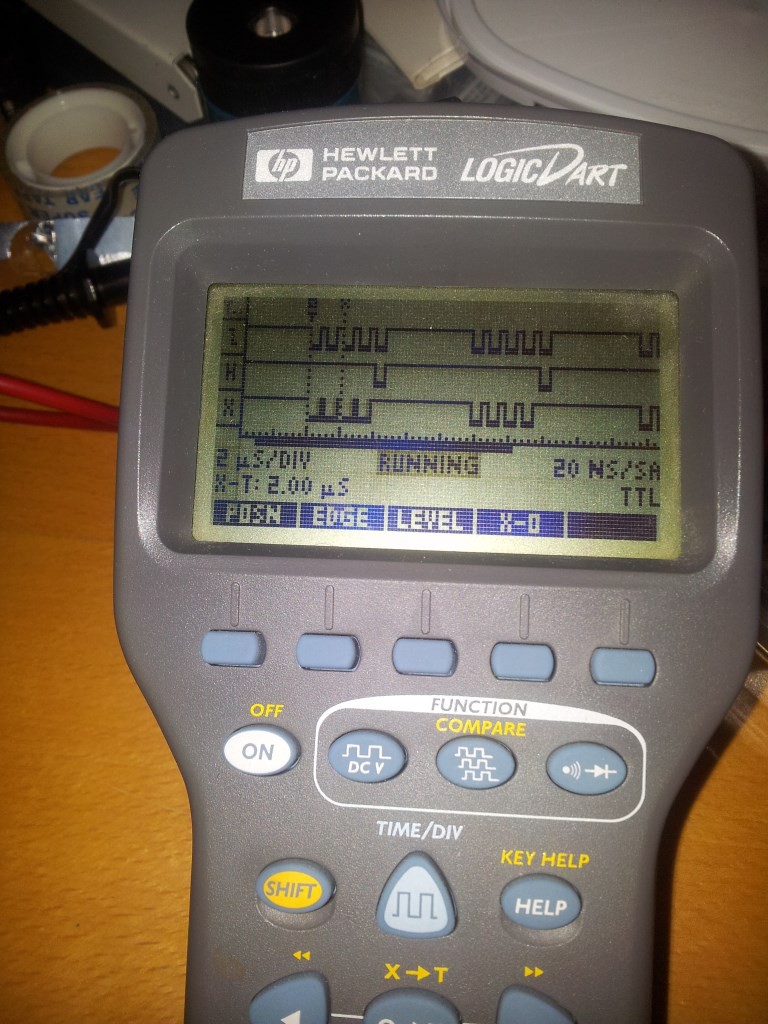
And here's the circuit behaving as expected, top line is the chip select from the RAM, indicating that A18 is set which happens during the write to memory, middle line is the chip select for the ROM, finally the bottom is the output on the led. This picture was taken while the LED was on, the pulse on the bottom line appears when the LED is on, and doesn't appear when it's off. It's not a very precise output but it's enough to show that the code and processor are working.
![]() Video of it working to come tomorrow, (potentially with my Arduino acting as a parallel to serial converter to print a Hello World message)
Video of it working to come tomorrow, (potentially with my Arduino acting as a parallel to serial converter to print a Hello World message) -
Odd Behaviours
06/09/2015 at 22:30 • 0 commentsWell sometimes it seems like it's working, but it only ever does half of what I expected. My initial attempt at getting visible output has been to use the A23 pin to blink an LED. I've gone through various iterations of the code, fixed bugs such as not have the the supervisor stack pointer in the ROM before the starting address. The problem I keep getting is yes the led blinks, and it even does it's pulses at seemingly the right time compared to the address strobe, but I can't control the rate at which it pulses. In the code I'm counting down d0 while writing to an address with A23 high, then I toggle A23 in the address and repeat the cycle. The problem being that changing the starting value from the count never affects the pulse rate. Another odd behavior noticed is that all the other address lines above A18 pulse at the same rate which makes little sense, they're all just floating (adding a pull down doesn't change it though) and the code is writing to address $840000 which should not be touching them.
    ORG    $0

    DC.l $0043000        ; Supervisor Stack Pointer
    DC.l start           ; Initial PC
start:
    movea.l #$840000, a0 ; Address of the first byte of ram
                         ; But with A23 set so it's written to LED
loop:
    move.l #10000, d0
delayloop:
    subi.l #1, d0
    move.b d0, (a0)
    cmpi.l #0, d0
    bne.s delayloop

    move.l a0, d1
    eori.l #$800000, d1
    move.l d1, a0

    jmp loop
In the picture below you can see what I mean by it seeming to work, the top row is the ~AS line, every time it goes low there's a valid address on the bus, the second is the ~chip select for the RAM, and the third the ~chip select for the ROM. It kind of makes sense there being 4 ROM accesses, then a RAM as the RAM is getting written to one in the loop. However there only being 4 ROM accesses doesn't seem quite right as I believe there should be 6 16-bit accesses in that loop, plus the 1 8-bit access to write to the RAM.![]()
I did some further experiments trying to read data straight off the bus using an Arduino and the A23 line as an interrupt trigger on the Arduino to latch. As well as trying to rig up some DTACK circuitry to make that more stable at triggering, I never quite succeeded as the Arduino was never quite triggering when I wanted it so I couldn't tell if the numbers that I sometimes got were the ones I was expecting or random noise.
At this point I'm tempted to re-wire the circuit, make a better halt/reset circuit with debounce so that I'm certain that it's reset correctly. Another idea may to be make a single step circuit to allow for easier debugging as I only have a 3 channel logic probe at the moment.
MC68000 Computer
My attempt at building a small computer based around a full Motorola 68000 processor.
 Well the breadboard part of my computer is no longer there. It's been all moved onto a single 3U euro-card sized protoboard. So I guess now I've got to change the title of the project. Was quite a bit of work to wire up the hundreds of point to point connections. All of it was done using 30AWG wire wrap wire, soldered point to point.
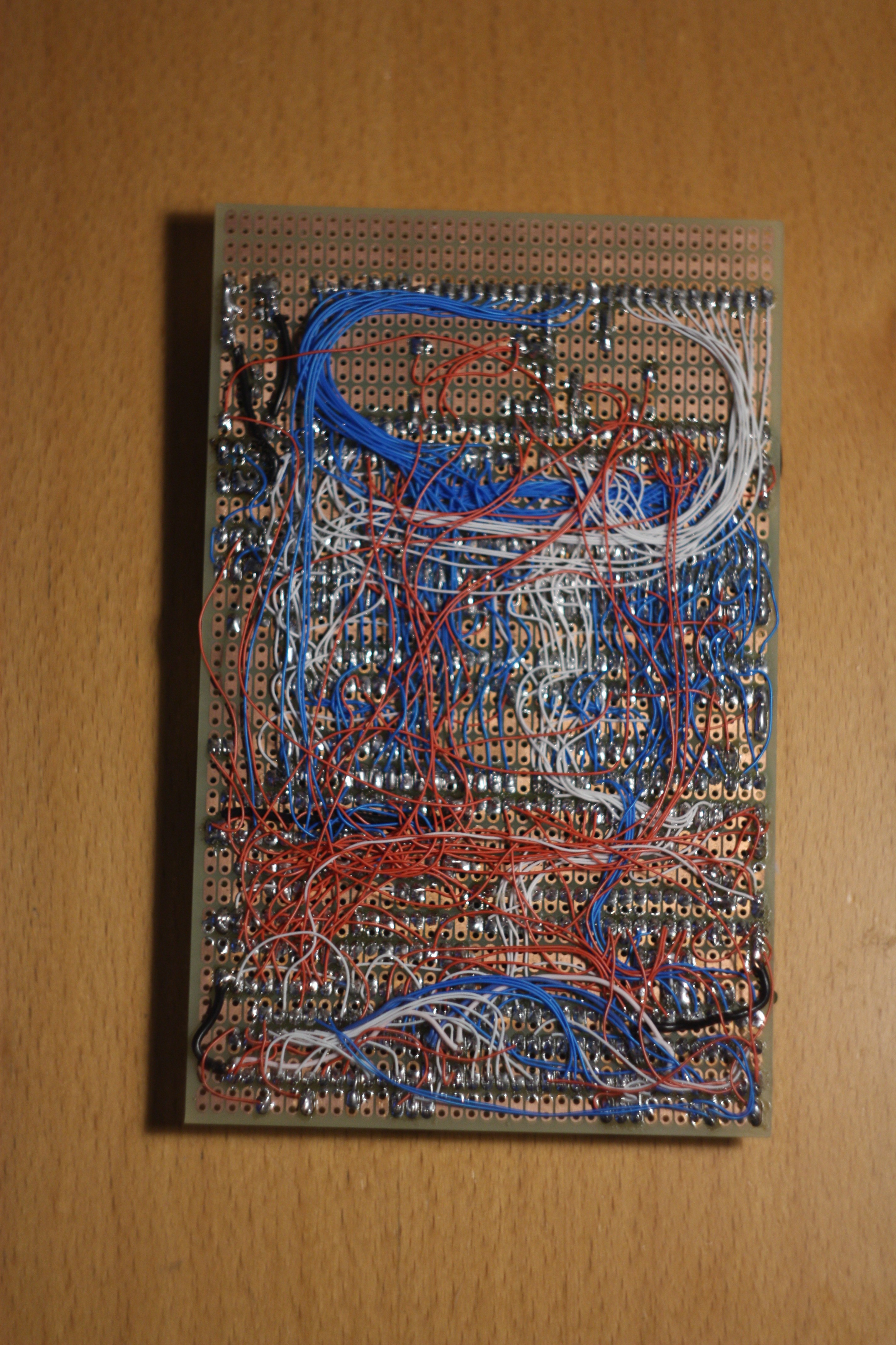
 Video of it working to come tomorrow, (potentially with my Arduino acting as a parallel to serial converter to print a Hello World message)