Quick and Dirty Parallel FLASH Programmer
Use an Arduino Mega and minimal parts to programme parallel FLASH.
Use an Arduino Mega and minimal parts to programme parallel FLASH.
To make the experience fit your profile, pick a username and tell us what interests you.
We found and based on your interests.
The hardware is simple enough to make rather quickly.
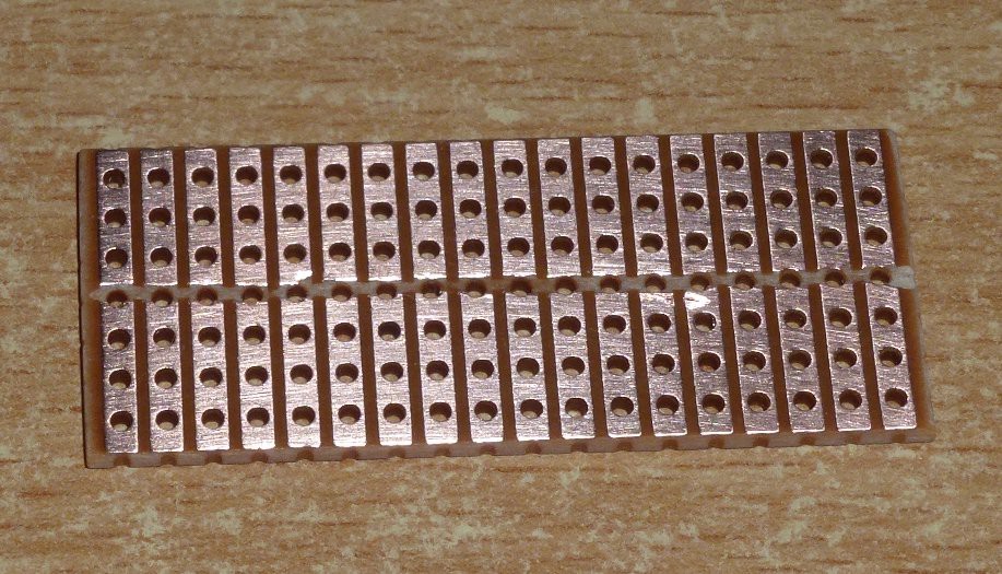
Cut a piece of strip (vero) board to size and cut a groove down the middle. I used a Dremel like tool to cut the gap.
Grab some right angle header pins and a dual row header. An old IDC socket like a hard drive IDE cable would do. 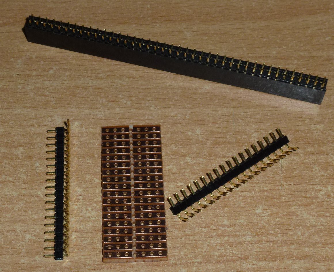
Remove the second last pin from the end of each row as shown. This is to stop Vcc and ground shorting to IO pins of the Mega.
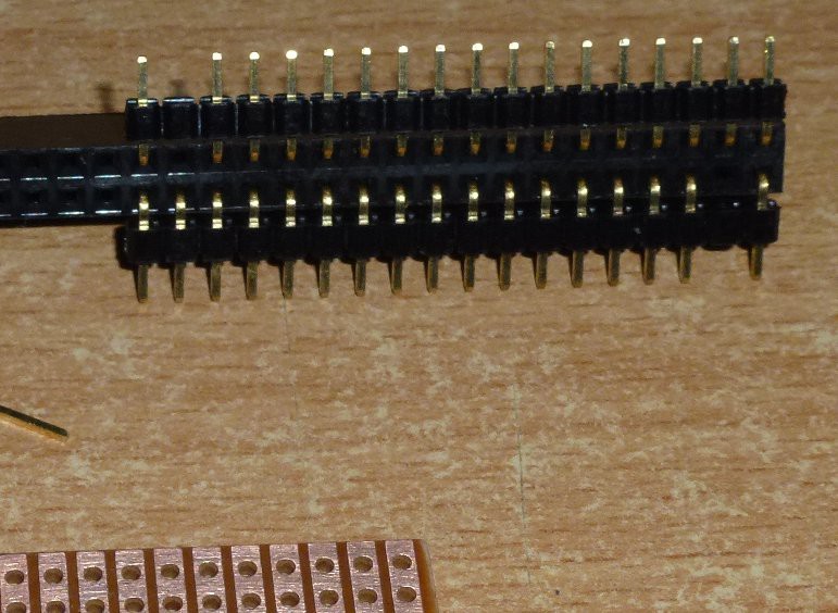
Now cut the pins shorter as they are too long and would cover the ZIF socket pins.
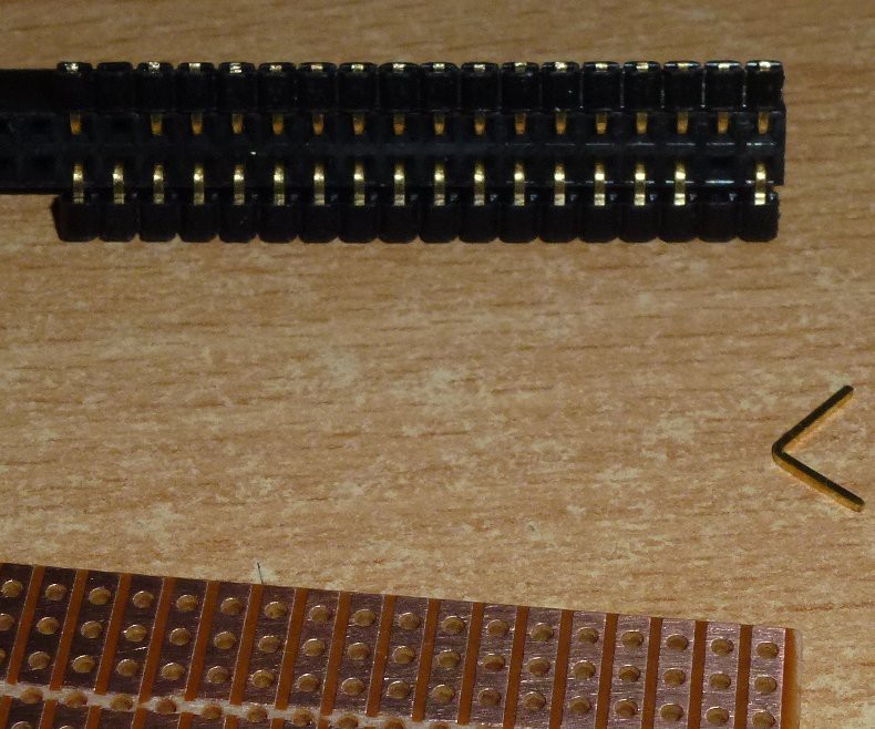
Remove the plastic strips from the pins. This takes a little patience. I ended up using a vice to hold it. then solder the whole thing to the strip board. Note the solder bridges at the ends for Vcc and ground.
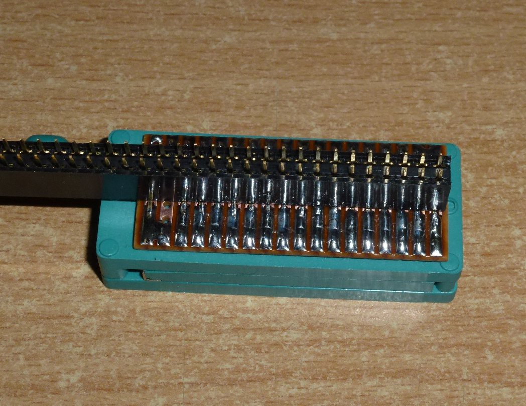
Now remove the header and check it over.
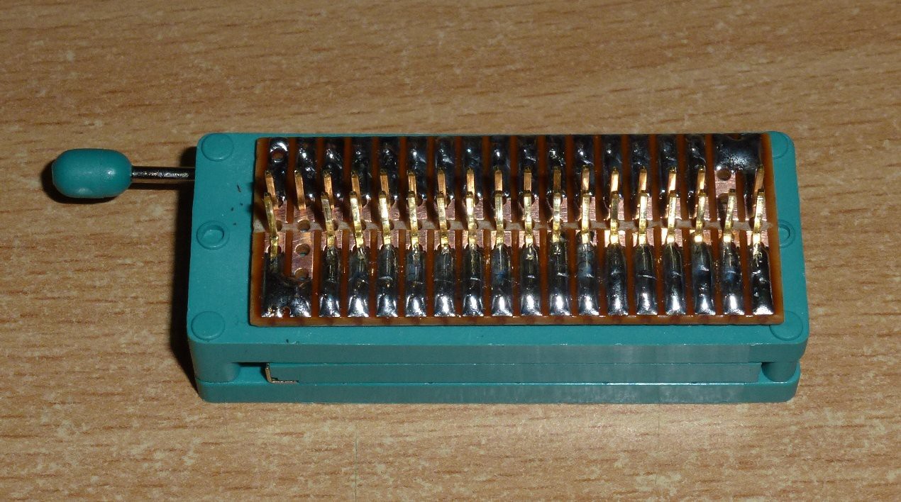
If all good then plug it into the Arduino Mega this way up -
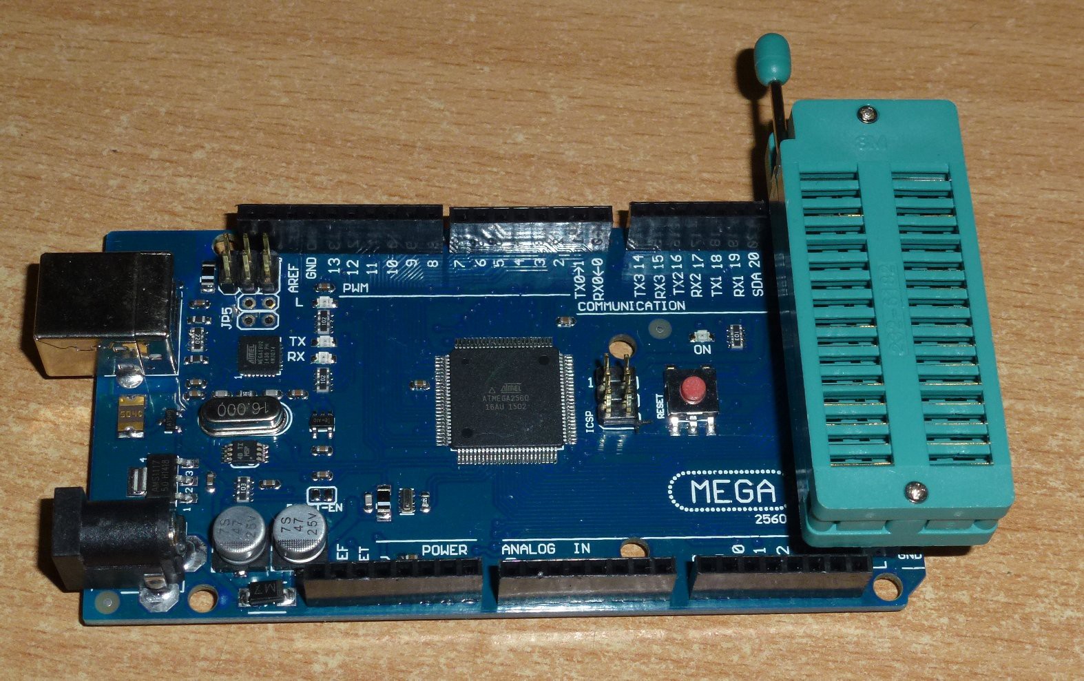
Ready to go -
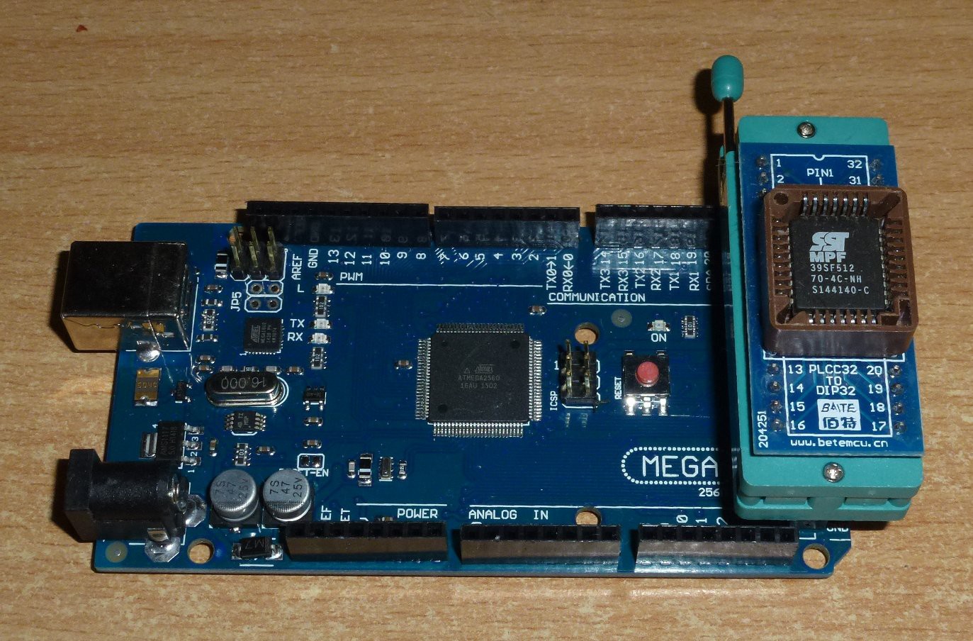
My next log will have the Arduino code (still don't know what Arduino code is called).
I already have the code done for a serial interface so I just have to port it over.
Create an account to leave a comment. Already have an account? Log In.
Dam it! I came here looking for the code because I have to program a 28 or 29 series EEPROM. So I guess there will be code for EEPROM and FLASH in 28 pin and 32 pin soon.
Ive been trying to do this kind of thing for a LOOONG time! I love how compact and pratical this is. I need to make one!
Been meaning to do something like this, myself... parallel flash chips (even in the MBs!) scrounged from old motherboards and whatnot could be quite handy for projects.
Cool job with the ZIF -> IDC layout!
yay ! I need something almost like that for the #Discrete YASEP :-)
The history seems to be -
1) Really old EEPROMS that couldn't be accidentaly written to because writing needed a higher (11.5v) Vcc.
2) Flash that was five volt programmable that needed 3 write per bit to prevent accidental writes from the CPU
3) LPC programming.
The parallel programming sequence is just some extra codes, like I mentioned it's about 3 writes to write 1 bite. I would suspect all parallel programmable FLASH has (at least) this feature and with the same code because there is a code there to read the manufactures ID code so there must then be cross manufacturer compatibility.
However some FLASH chips support *extra* features that may be manufacture specific, for example for some chips you can LOCK the whole FLASH chip and for others you have a finer grain control to lock specific sectors.
I agree with the AVR: speed/voltage thing. An ATmega328P-pu will run fine at 35MHz and at room temp (with an active oscillator, the internal won't do the higher speed). It's the temp range that is compromised by running them fast with a low Vcc.
I have seen lots of modern parallel FLASH on various circuit boards. The bit widths vary now and 8-bit is less common. Many of them are 16 bit or even 32 bit like modern SRAM. I still haven't seen any FLASH that is faster than about 70nS.
SD cards are good option when speed isn't needed as they're slow. You can solder them to a board and uses them like directly addressed FLASH but they have a higher write failure rate that the chips. There is also often the need for a file system and SD cards would be perfect for this.
I went through the junk room and here's what I found with PC tech -
Main boards have been using 3.3v BIOS PROMs (FLASH) for some time and there most often a PLCC32 chip soldered to the board.
Really old main boards used 5.0v chips in sockets (bingo!)
CD ROM drives more often use 5.0v PLCC32 chips and sometimes they're even socketed.
For the non-socketed chips - I put the whole CD ROM board upside down into a Pyrex bowl in the oven and heated it until the FLASH drooped off.
Most of the chips support Low Pin Count (LPC) programming but I didn't bother with that.
They also support write protection mode where you send sequences on the Address and Data buses / control and this is what I programmed for.
I don't know if the Arduino Mega will run 3.3v but some (small number) of 3.3v FLASH chips are 5 Volt tolerance.
The really old EPROM type chips need and extra voltage so they wouldn't
work this way.
Great findings. Hadn't heard of LPC programming, I'll have to look into that. The ("unlock"?) sequence is something I've wondered about, does it seem like it's standard amongst most devices, or do they differ?
The vast-majority of AVRs will do 3.3V... And if you're not doing mission-critical (product-design) stuff, they can usually run at their 5V-rated speeds even when running on 3.3V. If you've got an Arduino that's running at 5V it might not be too difficult to run it at 3.3, if necessary, maybe just replace (or add) a voltage-regulator. Or, the 74AHC-series (e.g. 74AHC245) are 5V-tolerant and great for level-shifting to 3.3V.
I've come across quite a few long-skinny-thin rectangular chips that have tiny-spaced pins on the ends (rather'n the sides) in the MegaBytes in things like DVD players and laptops that often are clearly marked "FLASH" in italics. Not nearly as mechanically-versatile as PLCCs, of course... actually, they'd be pretty difficult to solder-up without a dedicated PCB, and difficult even then. Nevermind, you'd have to program 'em in their end-circuit, rather'n before-hand. Maybe, at that point using an SD-card might be a wise path. OTOH, I think these chips use the regular-ol' address/data-bus interface that can be useful. I often desolder 'em with a heat-gun and some tweezers and throw 'em in a box, even though I've yet to use one...
The pins are all over the place. I just added the port pins below. I haven't yet done ATmega ASM so I just used the Arduino program to do one pin at a time. Is there a way to use C in the Arduino language to do ports as 8 bits/1 Byte? Although it's a couple of extra loops to get the buses out, it saves a lot of effort on the hardware side. I did a quick check of the port pins below but my sight isn't good so a second check would be advisable.
I haven't done C but it looks like any other curly bracket language but with strong type casting. I have to learn it yet but I don't know which type of C to start with.
ATmega FLASH Size / Pin Name
2560 IDE FLASH 512kB 256kB 128kB 64kB (kilo Bytes)
Pin Pin Pin 4Mb 2Mb 1Mb 512kb (kilo bits)
PA0 22 1 A18 NC NC NC
PA2 24 2 A16 . . NC
PA4 26 3 A15 . . .
PA6 28 4 A12 . . .
PC7 30 5 A7 . . .
PC5 32 6 A6 . . .
PC3 34 7 A5 . . .
PC1 36 8 A4 . . .
PD7 38 9 A3 . . .
PG1 40 10 A2 . . .
PL7 42 11 A1 . . .
PL5 44 12 A0 . . .
PL3 46 13 D0 . . .
PL1 48 14 D1 . . .
PB3 50 15 D2 . . .
16 GND . . .
32 VCC . . .
PA3 25 31 WE . . . *Active Low
PA5 27 30 A17 . NC NC
PA7 29 29 A14 . . .
PC6 31 28 A13 . . .
PC4 33 27 A8 . . .
PC2 35 26 A9 . . .
PC0 37 25 A11 . . .
PG2 39 24 OE . . . *Active Low
PG0 41 23 A10 . . .
PL6 43 22 CE . . . *Active Low
PL4 45 21 D7 . . .
PL2 47 20 D6 . . .
PL0 49 19 D5 . . .
PB2 51 18 D4 . . .
PB0 53 17 D3 . . .
These will straighten out if you copy it to a normal text editor. ie system font or fixed width font.
I just put the pin numbers into an array and index them out per bit.
// Hardware Platform specific parameters
int flash_address_pins[] = {44, 42, 40, 38, 36, 34, 32, 30, 33,
35, 41, 37, 28, 31, 29, 26, 24, 27, 22};
int flash_data_pins[] = {46, 48, 50, 53, 51, 49, 47, 45};
int flash_ce_pin = 43;
int flash_oe_pin = 39;
int flash_we_pin = 25;
One of the most valuable classes I've ever taken was Programming in C for engineering majors. These days it seems everything is descended from C, so knowing it makes picking up other languages much easier.
The Arduino environment makes use of the standard C AVR libraries. This makes it really easy to input/output bytes to GPIO pins in a single statement.
For output, set the Data Direction Register for the port/pins to 1, so to set all of the port A pins to output, use DDRA = 0xFF. For any pins configured as output, use PORTx to set their state. So PORTA = 0xFF would set all of the port A pins high.
For input, set DDR for the pins to 0, so to set all of port A to input, DDRA = 0. To read the state of the pins use PINx, so myVar = PINA. For any pins set as input, the PORTx register sets/clears the pull-up resistors.
Nice, I never thought of putting everything into that one header like that. Much more compact than the programmer I built.
How well did the pins on the flash line up with the ports on the ATMega? One of my OCD things is to always try to line up the data pins 0-7 with one of the ATMega's port's pins 0-7, so I can use direct I/O register read/write (rather than using Arduino's digitalWrite or trying to do bit math).
Become a member to follow this project and never miss any updates
By using our website and services, you expressly agree to the placement of our performance, functionality, and advertising cookies. Learn More
I made an adaptor for 28 Pin chips - the one here is for 32 - Pin.
I found parts of the code at different stages of development. Enough to get me going again.
One fork was using a CPLD to interface to the EEPROM/FLASH and loading the data code over serial Intel Hex.
The other fork is ATMEG2560 (Arduino Mega) in this project page that can hold 128kB (1 Mbit) in the code so it doesn't need serial. Larger chips can be done on blocks by using a start offset.
So hopefully I can do some coding on the weekend - I will be focusing on the AM28(C)xxx EEPROM and the SST39SFxxx FLASH but I will make the code adaptable without too much fuss.
I may be able to use DEFINE for chip parameters to save some SRAM in case someone wants to extend it.