I received the die hard dipsy kit yesterday (see here: https://hackaday.io/project/6592/log/23900-first-dipsy-diy-kit-shipped). It included two PCBs:
- one with a pre-soldered FPGA
- one bare PCB and fresh FPGA
The core voltage regulator (SOT-23) and 0402 resistors and capacitors (I was wrong about assuming they were 0201) were also included.
First board and blinky test
I couldn't reflow the pre-assembled board because the FPGA was already soldered, so I had to hand-solder the rest. It worked quite well.
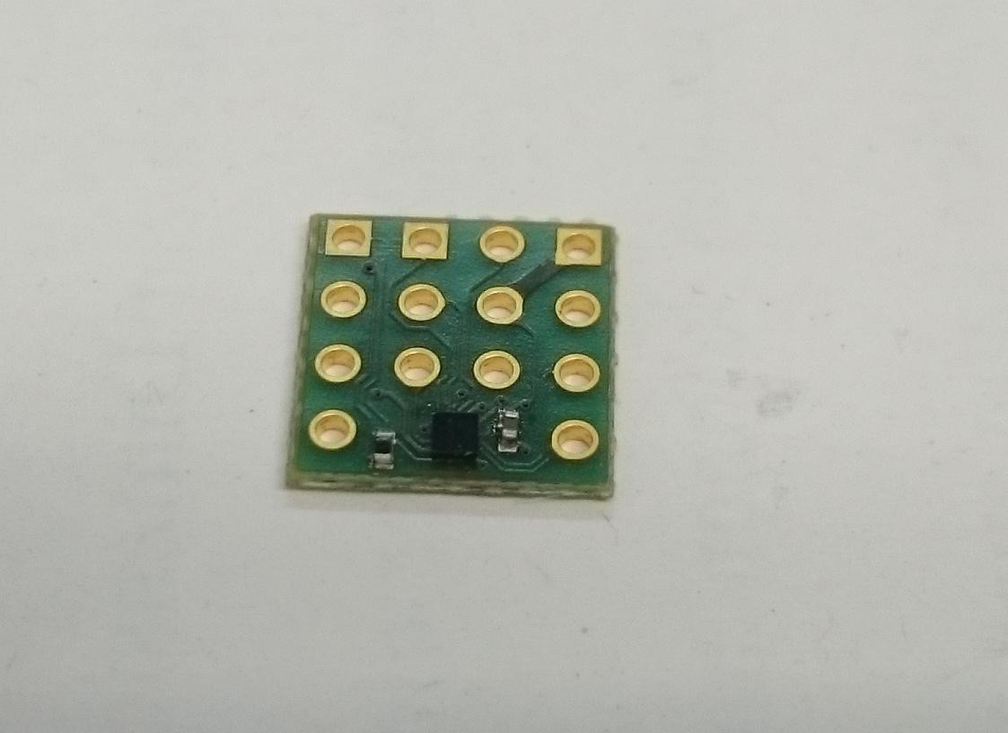
There are several ways to configure the FPGA, and one of them is volatile SRAM configuration. This means that an SPI master must transfer a configuration file to the FPGA after power-up, and the configuration won't be lost until the device is reset again. This was easy to implement on a Teensy 3.1, which has enough space to store the ~ 31 kB configuration file. Using Antti's AVR implementation, I got a first blinky. Here's the hardware:
Sorry, no video yet! More project logs on configuring the FPGA and first steps in VHDL will follow in the coming week.
Second board
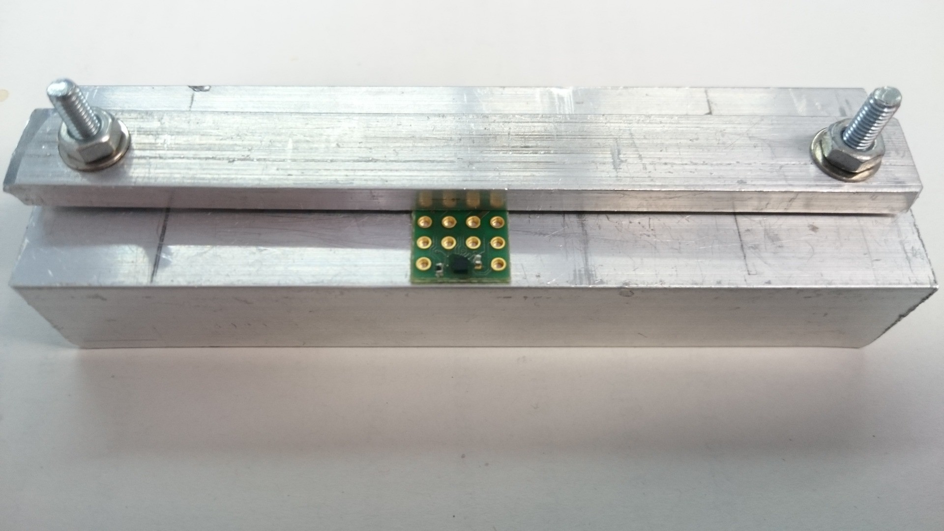
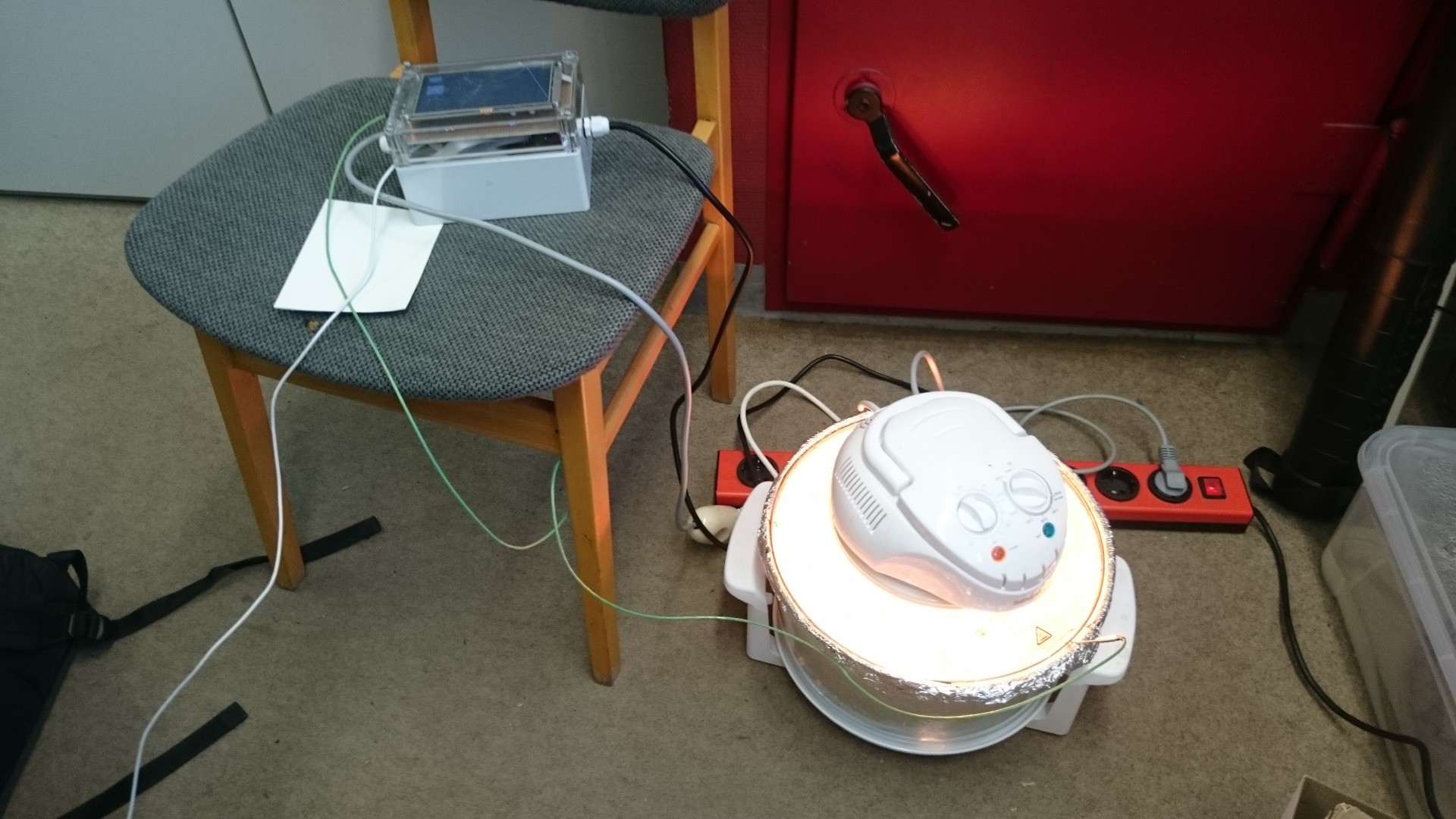
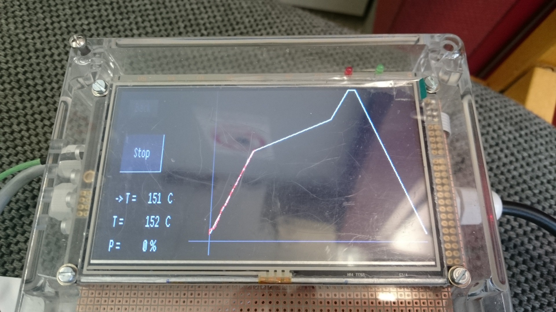
The second (bare) PCB could be reflowed. This was my first BGA and consequently the first BGA in my reflow oven.Applied a bit of flux to the BGA pads and solder paste for the passives, all components placed:
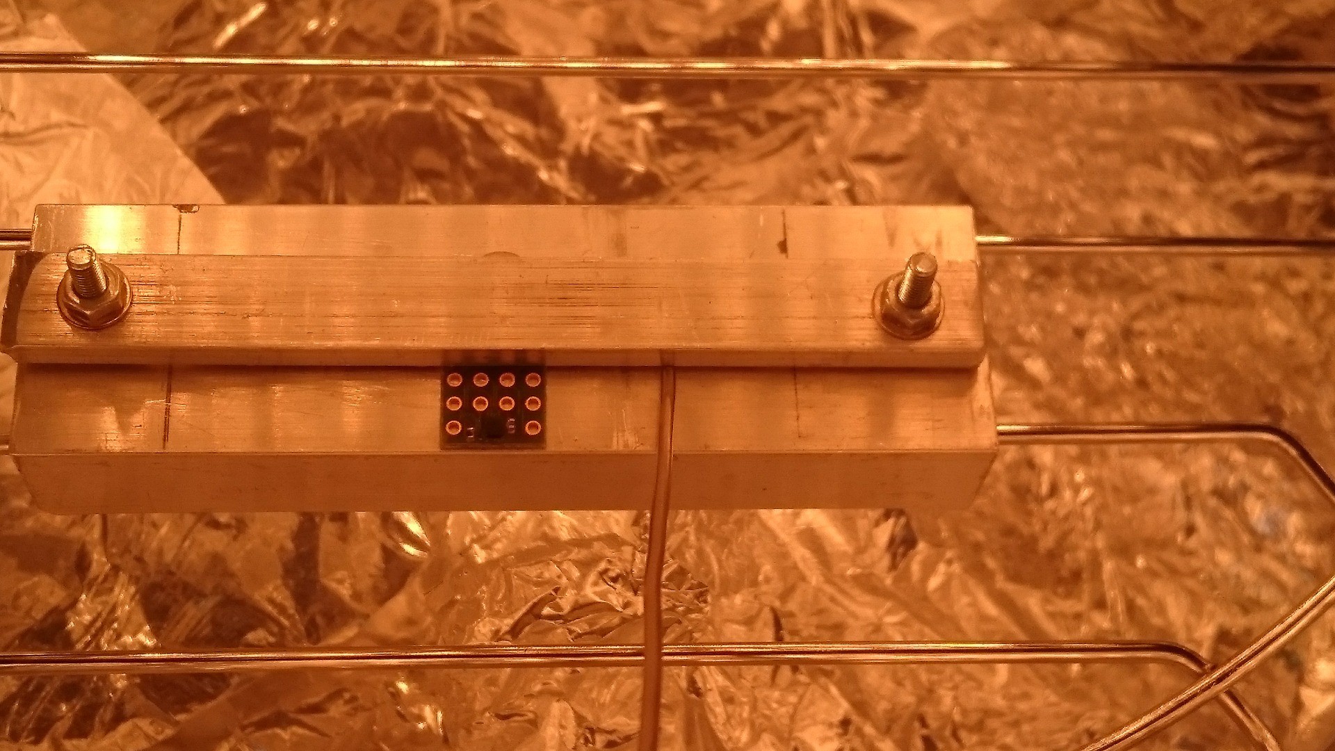
Result looks good:
Not tested yet, because I still need to add the bottom parts (one capacitor and the voltage regulator) manually. But I'm quite confident that the second board will work as well!
 Christoph
Discussions
Become a Hackaday.io Member
Create an account to leave a comment. Already have an account? Log In.
You are probably aware of this procedure, maybe for others - after soldering leadless packages, where I can't be sure whether everything is soldered properly, I use multimeter on diode test to check internal clamping diodes on IO pins against ground or Vdd lead, as I did it on #Pavapro - portable AVR programmer here
https://hackaday.io/project/3511-pavapro-portable-avr-programmer/log/12321-switching-on-the-soldering-iron-and-a-lot-of-pictures
I perform the test after soldering the leadless parts and before anything else, so it doesn't concide.
Are you sure? yes | no
Hey yes this is how it in most cases can be done, and how I tested first boards also. This is poor-man's "in circuit tester" methode !
Are you sure? yes | no
Successfully tested the outer pins (push-pull), they all have about 0.6...0.75 V. The inner open drain pins don't give any reading (neither in diode test mode nor in resistance mode), but I guess that's just architecture-related. The datasheet doesn't show too much detail about the I/O stage. I hope to find time for an in-circuit test later today.
Are you sure? yes | no
reverse the polarity of the multimeter in resistance mode, the LED I/O pins should also give some reading. Also GND-VCC gives some resistance reading.
Are you sure? yes | no
That's interesting about the open-drain IOs. I'd expect at least diode path between GND and the pin, resulting in ~0,7V reading in diode test DMM mode (not in resistance mode, there is usually too low voltage to open PN junction). Perhaps try to test from IO to VDD, if you tested from GND to IO before.
Are you sure? yes | no
tested the inner pins again in resistance mode with reversed polarity, and got some very high readings (10M) one some pins, and nothing on others. Might be related to the meter, though, it's not the best... I'll just try the dipsy later in circuit
Are you sure? yes | no
Wow!
Are you sure? yes | no
Wow2 ! This looks more pro then mines!
Are you sure? yes | no
Hey I haven't even tested the second one yet. Beauty doesn't matter if it doesn't work...
Are you sure? yes | no