Since I was born in mid-eighties, I've never experienced
real 74xx build. Few gates here and there was common, but lager designs were practically
unneeded - as microcontrollers, CPLDs or FPGAs replaced need for such as work.
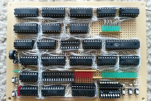
But my possession in vintage systems and desire to understand inner working
principles of modern devices brought me to design of simple CPU made of simple
74xx devices.
CPU design
CPU is not that complicated circuit, if we keep goals simple - so no hardware
multipliers, few registers, no fancy addressing modes. Such as CPU is not
particular useful, as even old 8080 outperforms this easily, but performance is
not primary goal now.
Basically, CPU does simple things - moving data from/to memory locations and
making operations on it. Program flow should be allowed to change and IO
latches are needed for real world operation.
Registers
Registers are elementary part of CPU design. They serve as most used and useful
memory locations, source or target of most of instructions. We will have a few
registers in our design.

Heart of register is latch 74HCT574. It latches data from data bus DB on rising
clock of WE signal. Passing this data to DB is controlled by OE signal, using
bus driver 74HCT245. Theoretically we can use OC signal of 574, but data should
be accessible even when output is not brought to DB. That is why two ICs are
needed to build single register.
We can have a lot of registers on single bus, with WE and OE signals for each
one register.
ALU
Adding ALU is quite simple task, thanks to 74181 developed in late 60's/start
of 70's. It is 4-bit wide ALU, capable of performing almost all common logical
and arithmetic operations.
Let's put two registers together, add 74181 and serve with single bus driver.

Nothing special here, but this starts to be quite useful. We have two registers
(A and B), controlled by respective OE and WE signals, ALU, with operation
controlled by signals on M and S1 to S4 signals (for more details see 74181
datasheet). Because 74181 doesn't have tristate outputs for connecting to DB,
bus driver is needed here. So, data in both registers (accessible from DB) can
be passed through ALU and put on DB again.
Imagine we want to do this sequence: put data to A, another data to B, perform
ALU operation and put into A again. We need to put A data on bus, assert and
release AWE, then put B data on bus, assert and release BWE. In the meantime,
ALU does its job (it is only combinational logic) and on F1 to F4 outputs is
result. We can assert ALUOE to put result on bus. To write it to A register,
asserting AWE is needed... but wait. If we assert WE, latched data (ALU result)
appears on data lines of A register, ALU changes its output and this is (or may
be) transferred to A register.
That's why third register is needed. Let’s call it T - temporary register.
After putting ALU content on bus, we write it to T register and then (when ALU
output is securely saved) to A register again.
PC
Let's focus now on another important part of CPU, program counter - PC. It's
main job is to increment whenever new instruction is needed or set to value
when program jump is to be made.

Nothing special again. Two chained 74HCT193 counters, EEPROM memory holding
program and instruction register (IR). It holds current instruction byte until
it is fully executed.
Preset inputs of counters (A, B, C and D) are connected to BD, in order to
allow direct change of PC (program jump). Otherwise PC changes after each
single instruction by CLOCK UP signal (pin 5).
Instruction decoder, part one
PC and registers with ALU are muscles of CPU, doing hard work, but it needs a
brain - to decide when and how to change control signals. Instruction decoder
does this job. Now starts the real fun and messing with 74xx logic.
Before actually building instruction decoder, it is necessary to decide which
instructions we are going to decode.
Instructions
For this computer, I decided to use only three instructions:
1, load direct data...
 jaromir.sukuba


 Szoftveres
 agp.cooper
 zpekic