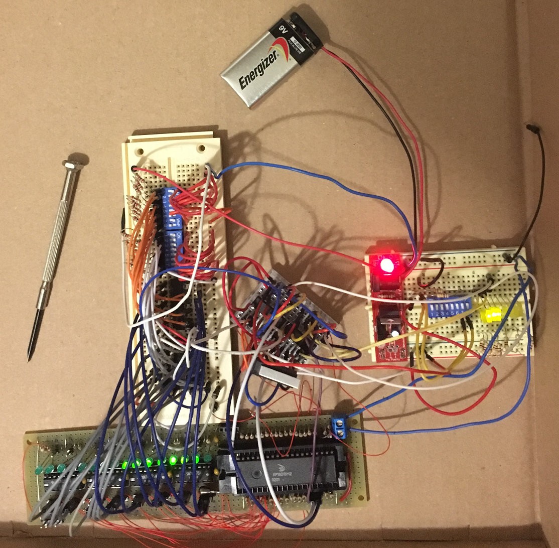
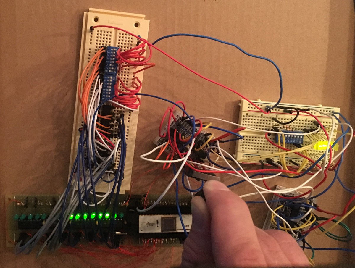
-
Possible videomodes
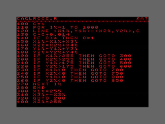
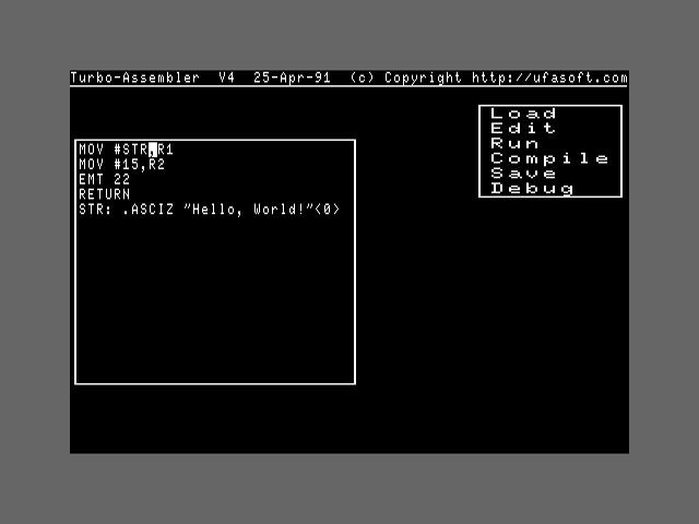
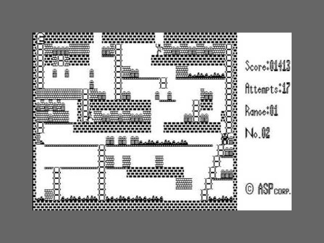
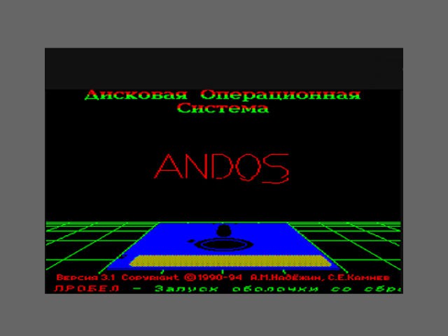
04/23/2018 at 09:20 • 0 commentsIdeally I want to be able to run not only text-oriented PDP-11 software, but also system and gaming software from Soviet BK-0011M home computer that had 512x256 monochrome video mode and 256x256 4-color video mode (with some predefined palettes). Output might be VGA with 2 resolutions - 640x350 (to display mentioned above 512x256 and 256x256 with some border space around) and 640x400 (to display "extended" video modes 640x200 monochrome and 320x200 4-color when every line will be shown twice by hardware) - both resolutions have the same pixelclock 25.175 MHz and the same field frequency 70.086 Hz. These are some photoshopped examples:
![]()
![]()
![]()
![]()
![]()
![]()
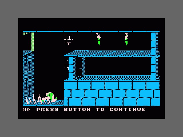
It was existing BK-0010 and BK-0011M software and now - new modes:
![]()
![]()
640x200 monochrome (first) and 320x200 4-color (second)
It's even possible to create very tricky videomode for 320x200 where every line may have its own 4-color palette...
-
Peculiar VM2 pipelining
04/23/2018 at 07:18 • 0 commentsFirst PDP-11 compatible chip in USSR named 1801VM1 was slow, so Soviet engineers decided to add instruction pipelining into next 1801VM2 to make it faster (microcode became so sophisticated that they left a few unnoticed holes in VM2 microcode which were patched only in later CMOS version 1806VM2). This is how I found out how VM2 pipelining works:
![]()
I wanted to know how many cycles this subroutine from Elektronika MK-85 will take (it's display clean procedure):
; clear screen

decimalnumbers

   org 0

.word   L0A34
.word   0

   org 0A34h
; 0A34:
L0A34:   mov   #80h,r0
; 0A38:
L0A38:   inc   r0
; 0A3A:
L0A3A:   clrb   07F80h(r0)
; 0A3E:
   clrb   (r0)+
; 0A40:
   bit   #7,r0
; 0A44:
   bne   L0A3A
; 0A46:
   cmp   r0,#0E0h
; 0A4A:
   bcs   L0A38
; 0A4C:
make_mk85_rom "clr.bin",32768
Program is compilable by PDP11ASM utility, but in my experiment I set every word manually by switches every time when new address is shown on address LEDs:
0003 0000                            decimalnumbers
0005 0000                               org 0
0007 0000 005064                     .word   L0A34
0008 0002 000000                     .word   0
0010 0004                               org 0A34h
0012 0A34 012700 000200              L0A34:   mov   #80h,r0
0014 0A38 005200                     L0A38:   inc   r0
0016 0A3A 105060 077600              L0A3A:   clrb   07F80h(r0)
0018 0A3E 105020                        clrb   (r0)+
0020 0A40 032700 000007                 bit   #7,r0
0022 0A44 001372                        bne   L0A3A
0024 0A46 020027 000340                 cmp   r0,#0E0h
0026 0A4A 103766                        bcs   L0A38
Below addresses are hexadecimal, but opcodes and arguments - octal (as usual for PDP-11):
0A34h 012700 mov #80h,r0 <<< 1st half (actual instruction opcode) took 8 cycles
0A36h 000200 <<< then 2nd half (argument 0x0080) took another 12, so it's 20 cycles total
0A38h 005200 inc r0 <<< increment of R0 took 8 cycles (now R0=0x0081)this is beginning of the loop:
0A3Ah 105060 clrb 07F80h(r0) <<< then clear BYTE memory location with offset R0 - 1st half took 8 cycles
0A3Ch 077600 <<< 2nd half (argument 0x7F80) took another 28 cycles (because it then goes to address 0x8001 to read word and then write modified word back), so it's 36 cycles totalat this point everything is logical and as expected, but then I observed a chaos:
0A3Eh 105020 clrb (r0)+ <<< it should clean BYTE by address R0 with post-increment, so we should expect read-modify-write from/to 0x0081 (current R0 value) - reading of opcode took 8 cycles
BUT THEN IT DOESN'T GO TO READ-WRITE FROM MEMORY - it goes to fetch next opcode!
0A40h 032700 bit #7,r0 <<< read next opcode in 8 cyclesthen we go to read argument 0x0007, right? WRONG! then it goes to finish previous command and perform READ-WRITE on address 0x0081! another 18 cycles
0A42h 000007 <<< and now we read argument 0x0007 - another 12 cycles
0A44h 001372 bne L0A3A <<< conditional branching opcode - 8 cycles to read
0A46h 020027 cmp r0,#0E0h <<< and then it reads NEXT OPCODE (just in case?) in 8 cycles, but this instruction will NOT be executed, because conditional branching was successful, so CPU doesn't bother to read argument 0x00E0 of that "just in case" instruction:0A48h 000340 <<< ignored
and jump - address indication shows 0x0A3A now...
So one run through loop is taking 36+26+20+8+8=98 cycles of CLCI - it's clearing 2 bytes in different parts of memory with post-increment of R0 and test that 3 less significant bits of R0 are not 0 to decide if it needs to continue (loop is intended to run through 96 bytes with skipping every 8th one).Per information from one knowledgeable person:
- 1801VM2 without dots on the package is capable of doing 12.5 MHz of CLCI
- 1801VM2 with 1 dot was tested on the factory with 10 MHz of CLCI
- 1801VM2 with 2 dots is worst from the series that was passed only 8 MHz test (but they recommend not go higher than 6 MHz for this kind)
Now you can estimate performance of your chip: 10-MHz one can do 1.25 million simple 8-cycle instructions per second and 12.5-MHz one - 1.5 million!
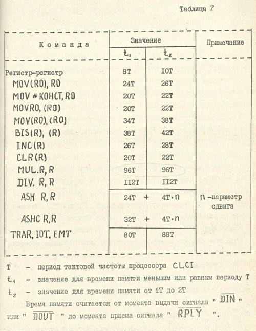
P.S. Actually my experiments with timings some sort of confirmed official VM2 documentation (in my case I didn't have delay between DIN/DOUT and RPLY at all, so it was 1st column):
![]()
P.P.S. Actually it is strange that VM2 does READ-MODIFY-WRITE cycle for clrb - it is NOT required, because PDP-11 is able to write half of the word (with WTBT=0 and A0=0 means lower byte and A0=1 means higher byte) and when we clear something we don't need to know what it was there before put 0 there... -
Experiments with KR1801VM2
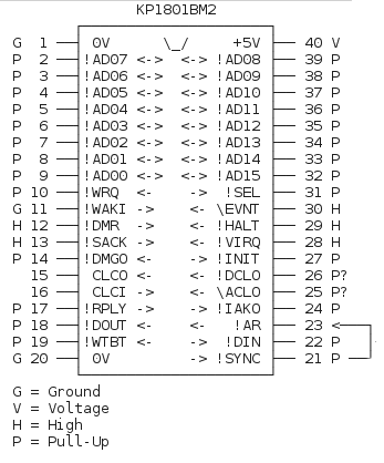
04/23/2018 at 06:09 • 2 commentsIt's time to explain experiments that I performed on actual 1801VM2 in February (some pics were in gallery since the beginning of this project without explanation). So it is important to know that most of VM2 pins have to be pulled up to +5V through resistors (I used 2K):
![]()
Here everything marked H and P are pulled up. G is grounded and V (pin 40) is actual +5V line:
![]()
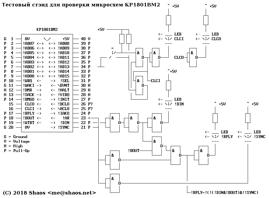
Then I decided to build a simple circuit to test VM2s by manual clocking through not existing memory (later I added a NOP instruction 0240 that is hexadecimal 0x00A0). Also PDP-11 architecture assumes a special handshake during reading and writing to support slow peripheral devices - on every !DIN and !DOUT external device must produce !READY triggered by !SYNC otherwise processor will go to trap subroutine after some number of cycles, so this is schematics that use three 74LS00 to generate !READY (without a delay - as fast as possible) and indicate on LEDs some important signals:
![]()
Clock is generated by manual pressing a switch button (because 1801VM2 has fully static design and may handle 0 Hz frequency) that goes to simple RS-trigger and then to CLCI input (pin 16) and indication through inverter (LED CLCI). CLCO output (pin 15) is CLCI frequency divided by 2 - it goes to indication as well (LED CLCO). 1801VM2 added another handshake that doesn't exist in PDP-11 - !AR that must be returned everytime when device catches address in the beginning of !SYNC - for simplicity !SYNC and !AR could be directly connected (see above pins 21 and 23). !SYNC goes to indication through inverter (LED !SYNC) and also used to generate !RPLY (pin 17) with help of !DIN (read control signal on pin 22) and !DOUT (write control signal on pin 18):
!RPLY = !(!(!DIN&!DOUT)&!!SYNC)
NOTE: In real application with interrupts also !IAKO should be used here, but we don't have interrupts for now so this simplification should be good enough to start.
Another handshake from PDP-11 is special procedure to power things up - after switching power on 2 signals !DCLO (BDCOK H in PDP-11 world) and !ACLO (BPOK H in PDP-11 world) must be low. Then !DCLO goes Hi (at least after 5 clocks CLCI from power on) and then !ACLO goes Hi (at least after 10 clocks CLCI from !DCLO went up) - here I simply used 2 grounded wires that I manually connected to pulled-up pins 25 and 26 in proper order after some number of clocks.
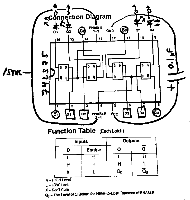
Also I added address latch on 4 chips 74LS75 that stores address from AD lines in the beginning of !SYNC to show it on LEDs and use in future when actual memory is connected:
![]()
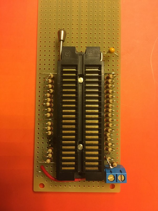
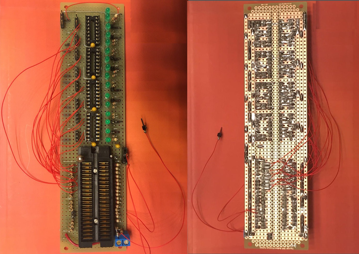
Here D1-D4 are four AD-lines from VM2 and !Q1-!Q4 are inverted latched address bits that were inverted so it's not inverted anymore (and Q1-Q4 go to indication and stay inverted). This is a board with ZIF socket (and I should be honest - inserting Russian chip with metric pitch there was a little problematic):
![]()
![]()
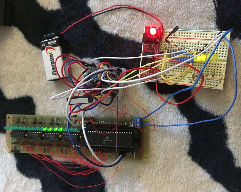
First test (circuit was even simpler that time - it used only 2 74LS00):
![]()
I put results of initial start in Wavedrom to make it more visible:
![]()
You can see !DIN goes down 3 times - 1st time without !SYNC when it's reading starting vector from external circuit - because nothing is there and AD lines are pulled up it reads 0xFFFF inverted or 0x0000, so it assumes that starting address and flags are stored in address 0x0000 so then it reads address as a word from 0x0000 (2nd !DIN) and then flags as a word from 0x0002 (3rd !DIN).
Then I added 2 buffers 74ALS240 with 16 switches to imitate memory response on reading to have NOP instruction 0240 (hexadecimal 0x00A0) be on data bus when !DIN is down to turn VM2 into counter:
![]()
At this point I was able to test all my VM2 chips - I assumed SUCCESS if chip was able to run at least to address #00FE (0000000011111110) - as pictured above. So from 4 black (plastic) KR1801VM2 (КР1801ВМ2 1992 & 1993) ALL were good! But, from 6 white (ceramic) KM1801VM2 (КМ1801ВМ2 1989 & 1990) only ONE was good :(
![]()
TO BE CONTINUED
-
PDPii.com
03/09/2018 at 06:16 • 0 commentsI just registered domain name pdpii.com ;)
Now I'm thinking about a family of modules (main processor one and many peripherals) that shares the same bus ( breadboard friendly Q-bus extended or BBFQ-bus+ ; ) - all open source of course :)
Using such modules anybody should be able to build "oversimplified" PDP-11 compatible machine or PDPii...
 SHAOS
SHAOS