-
Separate Project for Hackaday Prize
04/22/2019 at 04:48 • 0 commentsIn order to be able to participate in HacladayPrize2019 I created separate project #PDPjr that will be focused on creating simplified (but still usable) version of PDPii so please LIKE that project as much as you LIKE this one ;)
-
Hello, World!
03/20/2019 at 05:57 • 0 commentsI don't have backplane yet, so I can use breadboard instead ( it is Bread Board friendly Q-bus after all ; )
![]()
Couple yellow diagonal wires on the left are for BDMGO-BDMGI and BIAKO-BIAKI deasy-chains.
![]()
Actually if CPU module is the last board then those two wires should be rotated, because CPU generates both BDMGO and BIAKO so they should go from right-top to bottom-left, but for now it doesn't matter because we don't use DMA or interrupts...
Now we will try to do something with LCD 16x2 that has 8-bit parallel interface. Simple circuits from 74LS32 OR-gates and couple 74LS374 registers does the trick - by writing to address 0xFF00 it will store 16-bit value on registers to be used to control LCD. Important thing when you are playing with LCD is delay between commands during LCD initialization and work that should be long enough for LCD to work properly. To implement precise delays we will use PDP-11 instruction sob (subtract 1 and branch if not equal to 0):
    mov #100,r0 ; 100 cycles of sob
delay1:
    sob r0,delay1
Step-by-step run of the 1st draft of the test program showed that 1 cycle takes 24 CLCI ticks (8 ticks to read sob instruction from memory, another 8 ticks to read NEXT instruction and then another 8 to execute branch), so we can easily compute for how long we should cycle to perform 15ms, 5ms and 1ms delays:
decimalnumbers
    org 0
    .word 0100H,0E0H ; reset vector
    org 0100H
start:
    mov #12500,r0 ; delay 15 ms for 20 MHz
delay0:
    sob r0,delay0
    mov #init,r4
initloop:
    movb (r4)+,r0
    beq endinit
    com r0 ; invert character
    bis #0FF00H,r0 ; set all bits of higher byte
    mov r0,@#0FF00H
    bic #800H,r0 ; inverted E=1
    mov r0,@#0FF00H
    bis #800H,r0 ; inverted E=0
    mov r0,@#0FF00H
    mov #4167,r0 ; delay 5 ms for 20 MHz
delay1:
    sob r0,delay1
    jmp initloop
endinit:
    mov #msg,r4
loop:
    movb (r4)+,r0
    beq endloop
    com r0 ; invert character
    bis #0FF00H,r0 ; set all bits of higher byte
    bic #200H,r0 ; inverted RS=1
    mov r0,@#0FF00H
    bic #800H,r0 ; inverted E=1
    mov r0,@#0FF00H
    bis #800H,r0 ; inverted E=0
    mov r0,@#0FF00H
    mov #833,r0 ; delay 1 ms for 20 MHz
delay2:
    sob r0,delay2
    jmp loop
endloop:
    mov #0FFFFH,r0
delay:
    sob r0,delay
    jmp start

msg:    .byte    "Hello, World!!!",0
init:    .byte    30H,30H,38H,8H,1H,6H,0CH,0
As I wrote before I have one strange VM2 that is capable of running on 20 MHz and it says "Hello, World!!!" now :)
But I see that 20 MHz is too much for VM2 anyway - it is glitching and eventually stops showing anything meaningful on LCD. Lower frequency 16 MHz is much more stable (no glitches)...
-
NOP test with ROM module
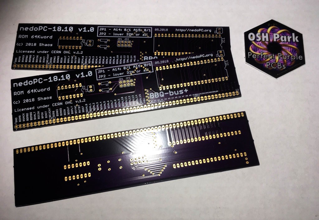
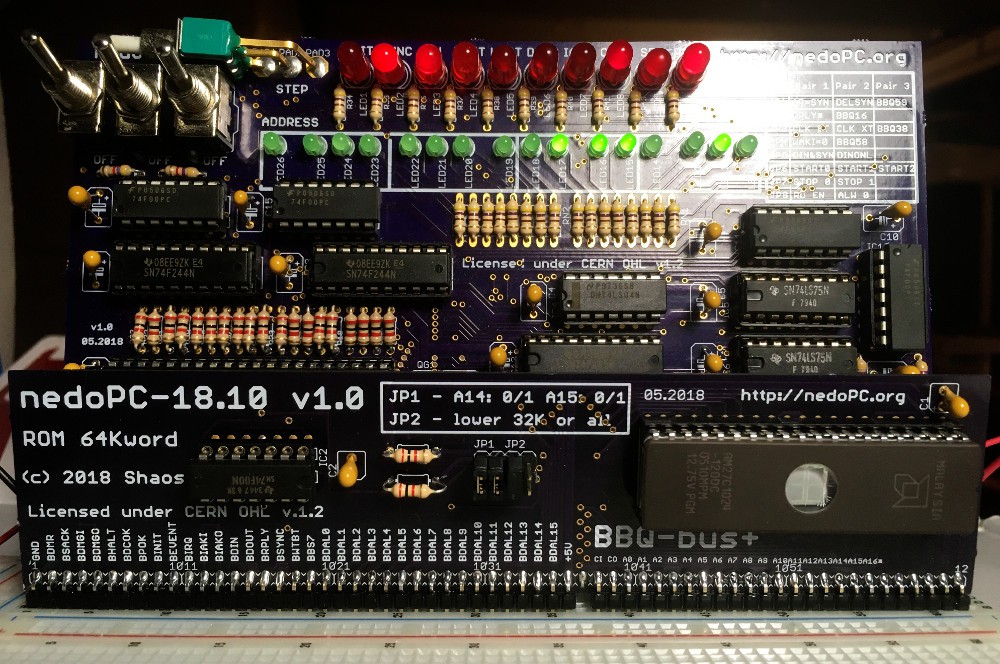
03/16/2019 at 06:19 • 0 commentsA few days ago I received 3 PCBs from OSHPark:
![]()
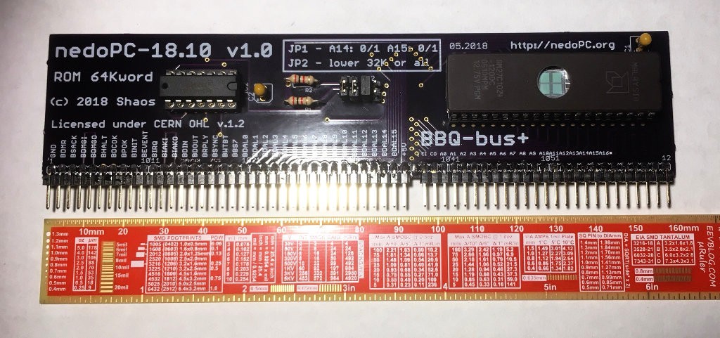
and today built one of them:
![]()
It could be inserted into large solderless breadboard together with CPU module for testing without backplane:
![]()
I flashed ROM with very simple program - a lot of NOP instructions (for PDP-11 it is word 0240 or 0x00A0 that should be inverted and stored to ROM as 0xFF5F because our databus in PDPii is inverted). With 1 MHz oscillator we see this:
It is possible to calculate that most significant address LED (green one on the left) blinks about every 0.4 seconds and it sounds about right because 1 NOP is 12 external ticks (6 internal) and 32768 NOPs (whole address space) with 1 MHz external clock should be done in 1/(1000000/12/32768)=0.39 sec.
Now I should write something more complex for it ;)
P.S. Also I successfully tried 3 MHz, 4 MHz and 10 MHz oscillators on black VM2s with 1 dot on the package (rated 10 MHz on the factory), but higher frequencies expectedly failed to work (namely 16 MHz and 20 MHz).
P.P.S. Black VM2s without dots (highest rated) appear to be working with 16 MHz oscillator!!!
P.P.P.S. One recently bought black КР1801ВМ2 with dot (so it has to be <=10MHz) worked not only on 16 MHz, but even looked functioning on 20 MHz ( but not 25 ; )
-
CPU module testing without memory
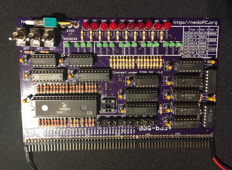
05/21/2018 at 05:56 • 0 commentsAs I already wrote before, CPU module alone could be used to test 1801VM2 CPUs - with manual clock (when user presses button periodically) and without memory (databus always returns all zeros). This board was tested today:
![]()
This is video in 1080p60 mode:
and this is a success! ;)
![]()
-
CPU module PCB built
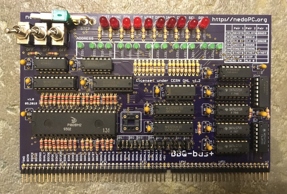
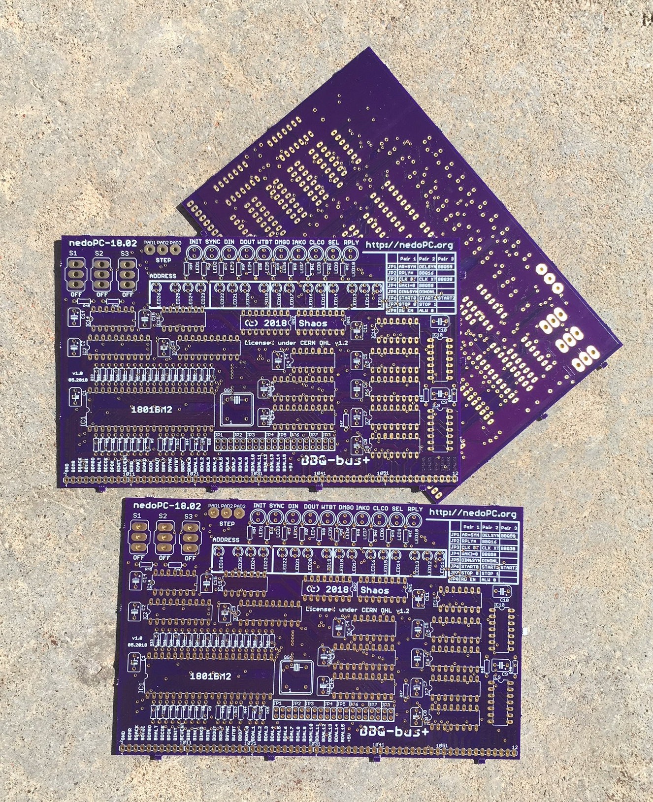
05/13/2018 at 05:11 • 0 commentsA few days ago I received 3 PCBs from OSHPark:
![]()
and today built one of them:
![]()
for testing purposes all ICs have sockets - now it's time to test :)
![]()
-
Live video of RAM module making
05/12/2018 at 04:49 • 5 commentsLive video stream 1280x720 from my PowerPC G4 laptop ended - speed-up video is here:
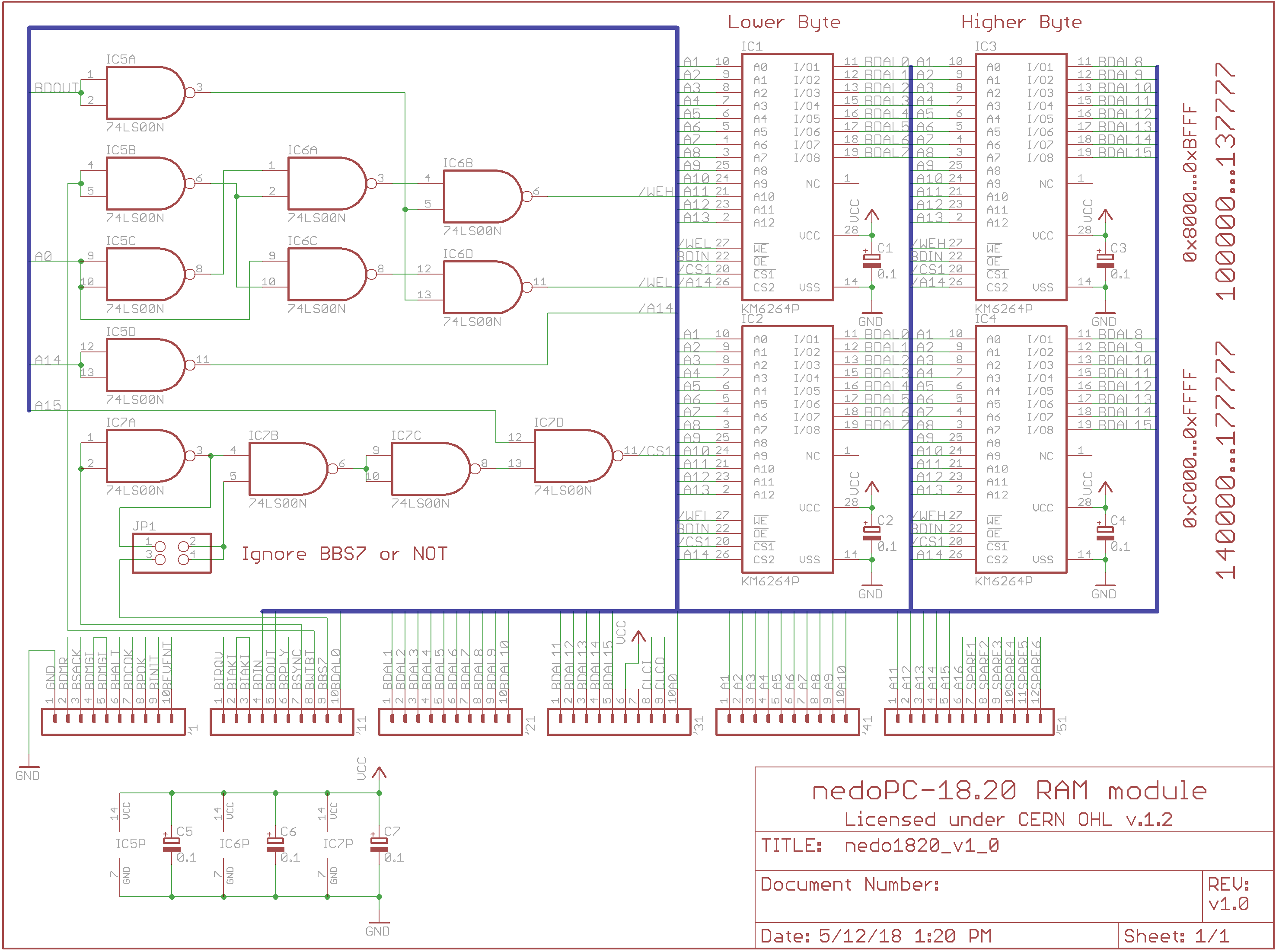
This is a result of almost 6-hour work:
![]()
![]()
ZIP with SCH and BRD uploaded to Files
-
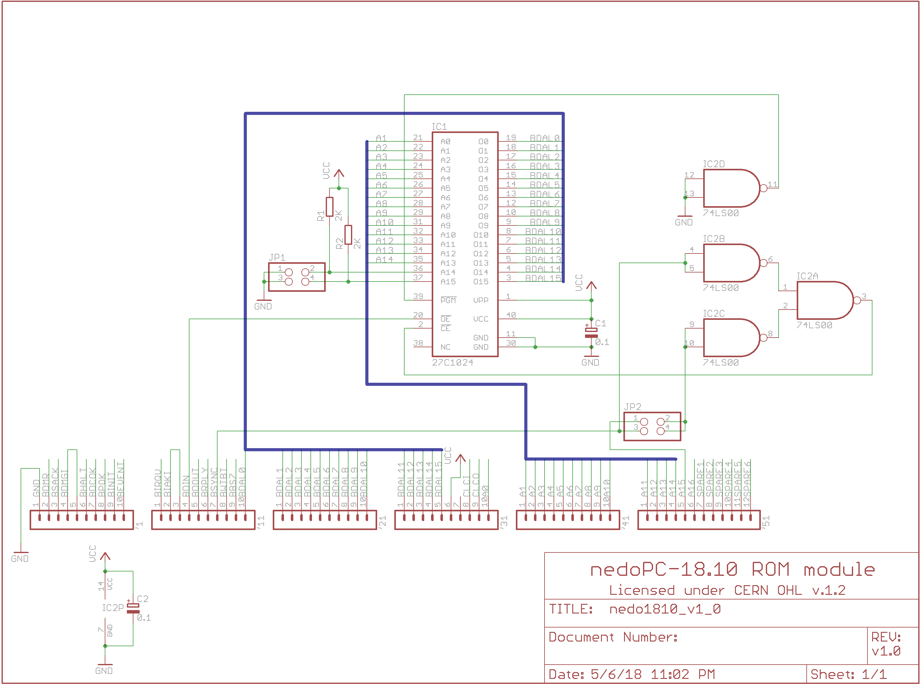
Live video of ROM module making
05/06/2018 at 03:56 • 11 commentsI live streamed creation of ROM module board in Eagle v5 running in MacOS X 10.4 on the one of the latest PowerPC G4 laptops that I own since 2007 ;)
Later I edited archived videos to remove pauses and made it 8x faster:
Results (ROM 64K board) added to GitHub and here in Files:
![]()
![]()
-
Board templates
05/05/2018 at 15:38 • 0 commentsI added board templates here and at GitHub repository (moved to GitLab in June 2018)
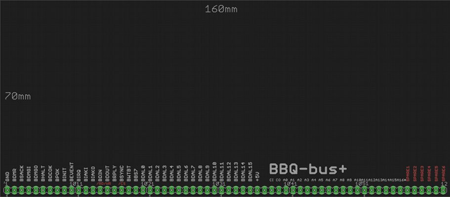
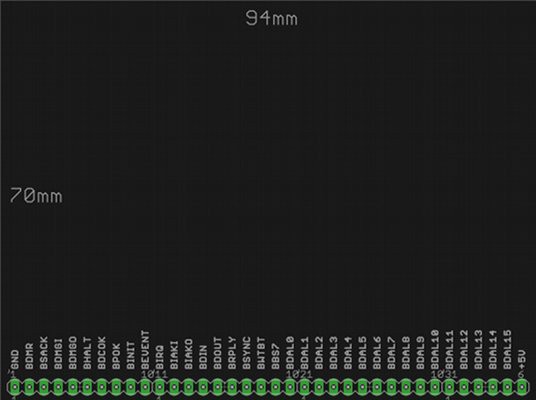
![]()
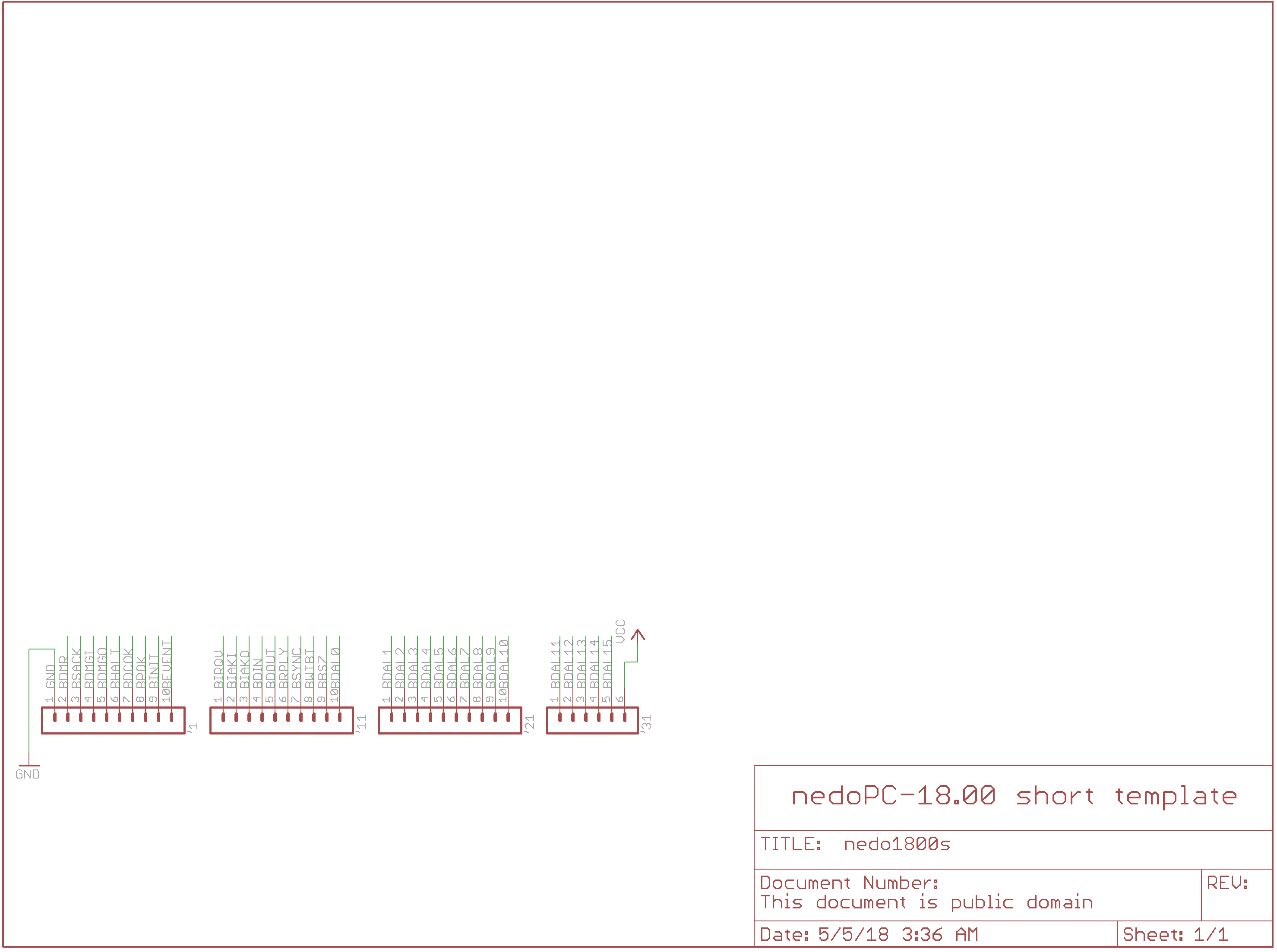
it's full size board with height 70mm to make sure it fits under the power supply in mini-ITX computer case. Schematics have just header in it and nothing else:
![]()
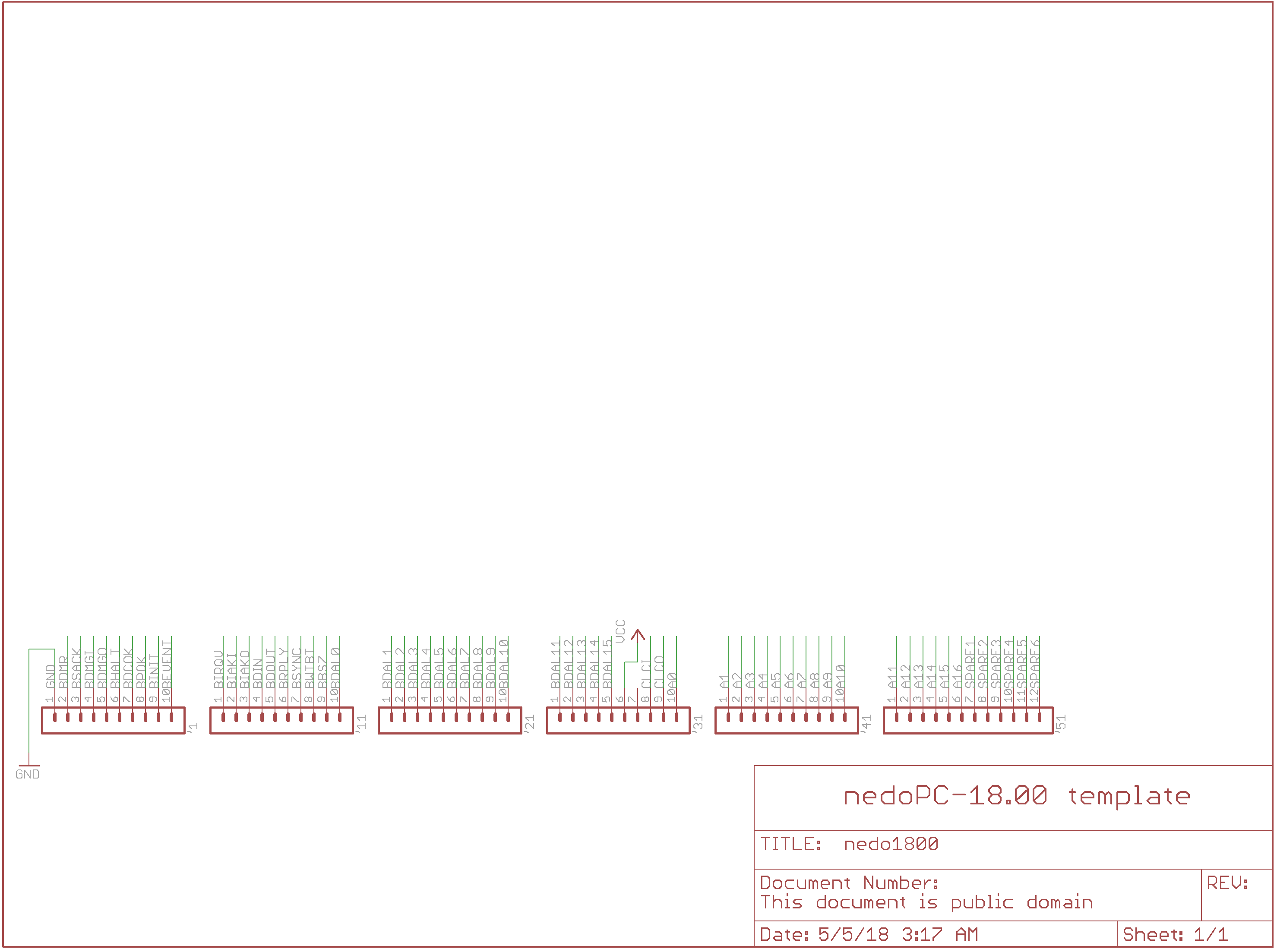
Shorter version, that use only Q-bus part of BBQ-bus+ interface (and fits into limits of Eagle v5 free edition):![]() Schematics:
Schematics:![]() Here you need to do address latch on your own, but PCB might be much smaller.
Here you need to do address latch on your own, but PCB might be much smaller.
Also in both cases if you don't use DMA or interrupts then you should connect BDMGI to BDMGO and BIAKI to BIAKO to make sure those daisy chains are keep functioning for the next boards connected to backplane after your board. -
CPU module PCB ordered
05/02/2018 at 04:05 • 5 commentsCPU module v1.0 was ordered through OSHPark:
![]()
![]()
SCH and BRD files for Eagle v5 attached in Files section:
https://cdn.hackaday.io/files/673692882315296/nedo1802_v1_0.zipand also uploaded to GitHub and later moved to GitLab:
-
Working on CPU module
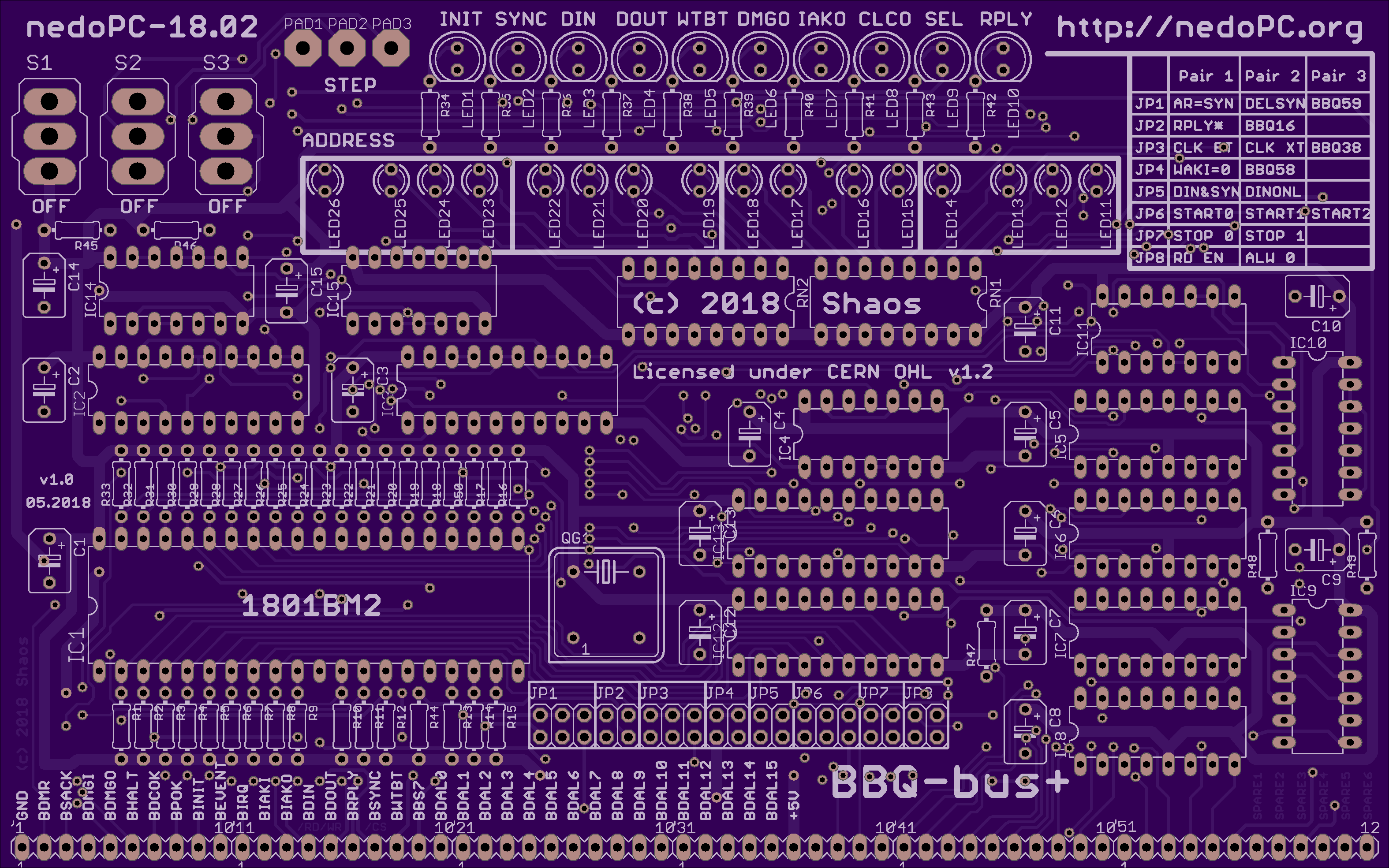
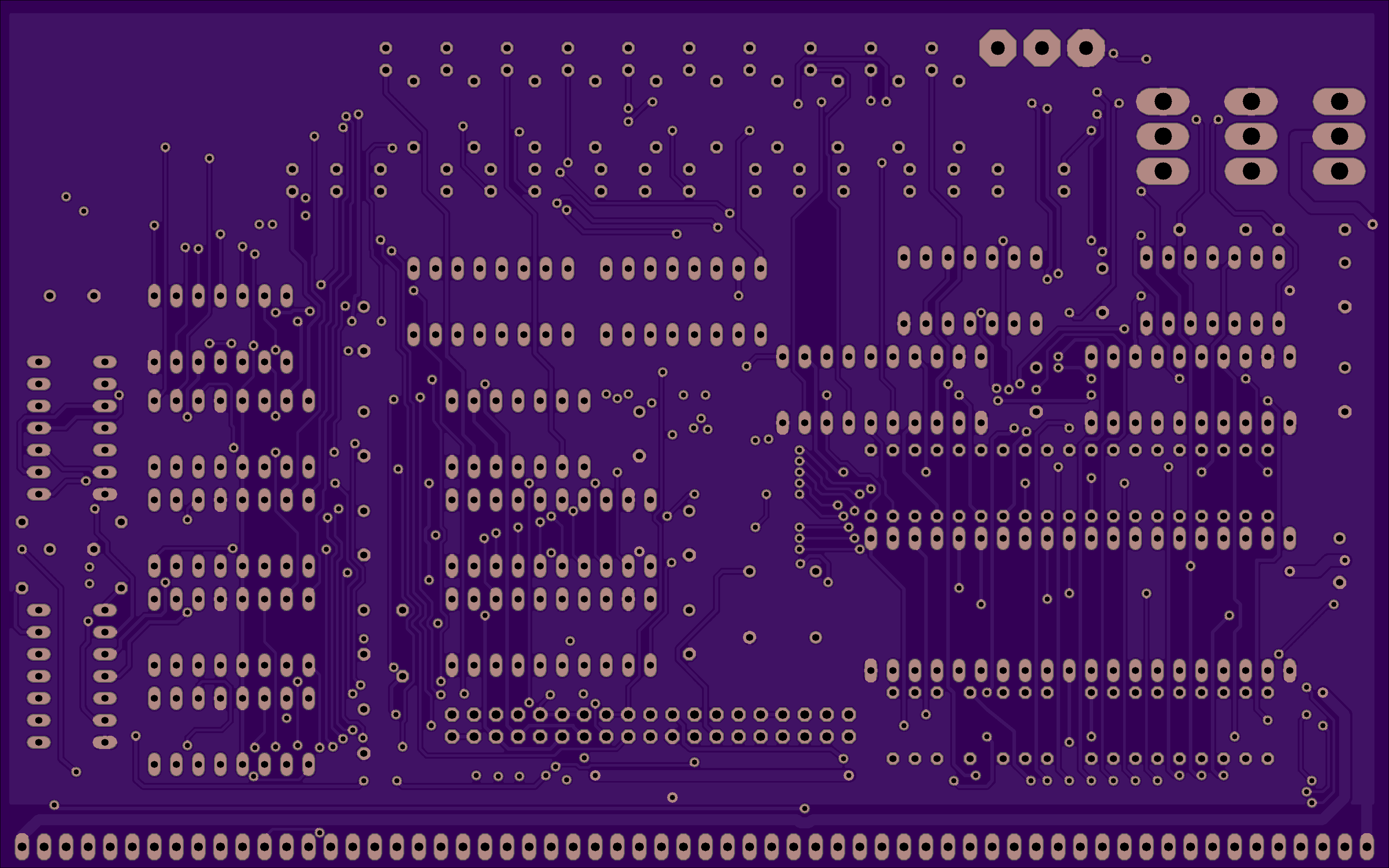
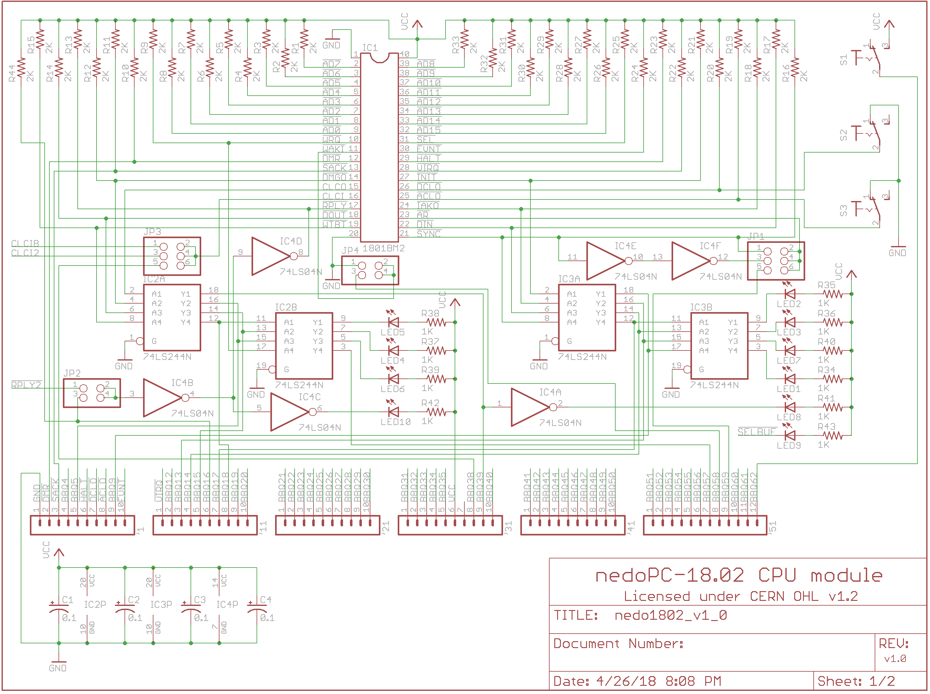
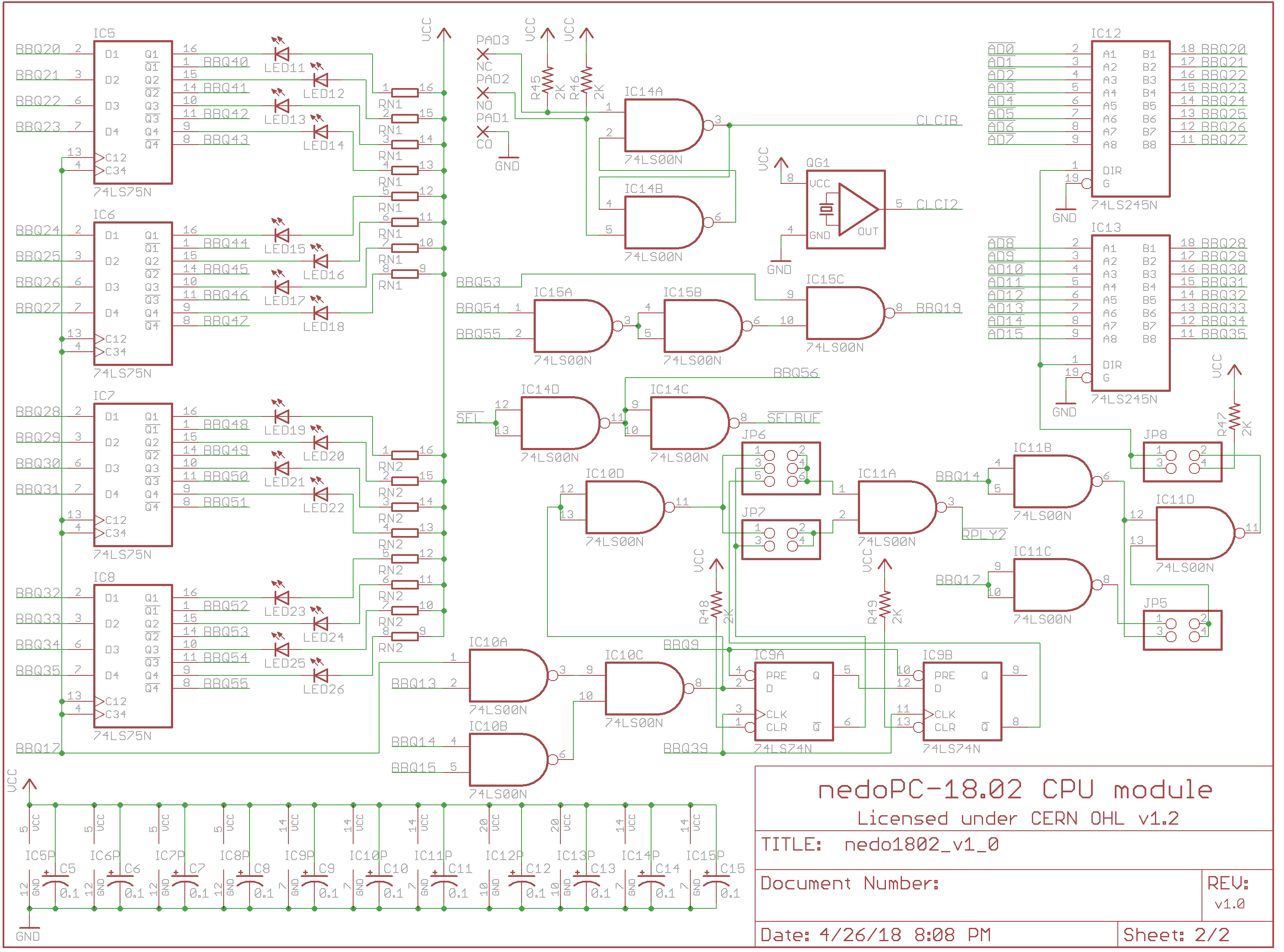
04/27/2018 at 06:36 • 0 comments1st module that I'm trying to create right now is CPU module with 1801VM2 onboard - I'm buffering everything (VM2 pins are very weak) and also this module has address decoding and indication for some important signals:
![]()
CPU might be clocked by button, by TTL oscillator or by external clock (CLCI):
![]()
Board will look like this (160x100 mm):
![]()
It could be vertically inserted into mini-ITX backplane (not yet designed), but also might be used as a standalone VM2 tester
BTW thanks to OSHPark for rendering this image ;)
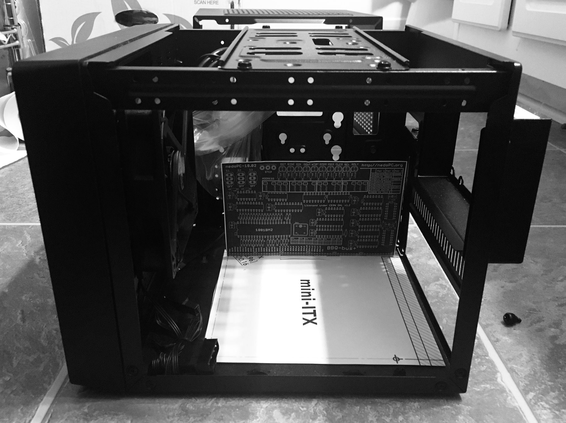
Printed it on paper to see how it may fit into mini-ITX computer case:
![]()
As you can see CPU module is a little too high - power adapter will not allow to put it in most of the slots of mini-ITX backplane but if it will be the last board (as pictured above), it should be ok, because power adapter is a little bit shorter than mini-ITX board and we have some free space there on the side...
 SHAOS
SHAOS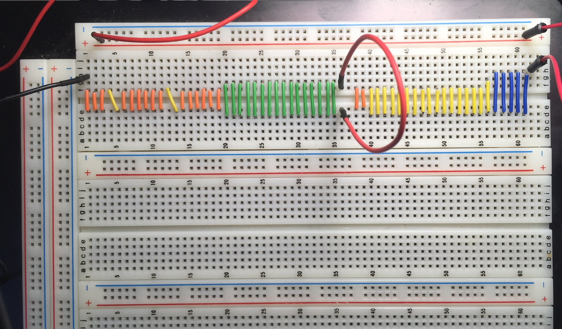





 Schematics:
 Here you need to do address latch on your own, but PCB might be much smaller.