Ted Yapo
-
The Rise and Fall of 74LVC1G04
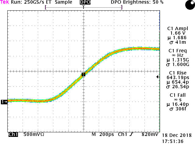
12/18/2018 at 23:21 • 0 commentsRise and fall times, that is. I have finally been able to measure the rise and fall time of these fast little single-gate packages. I was previously limited by the 1.2ns rise time of my old scope, but I suspected they were faster than that. Now, I have proof. The rise time is around 650ps and the fall 460ps. That's pretty fast.
![]()
This gate is being run at 3.3V with a 47-ohm series termination resistor through a short cable into a 50-ohm terminated scope channel. The waveform looks pretty good.
![]()
I have some 74AUC1G04 gates ordered, which have a shorter propagation delay, but I'm not sure about the edges. They supposedly use some kind of 3-mode output stage that dynamically changes its impedance to drive lines accurately. Or something like that; the datasheet isn't very specific. -
One blue wire: 296 MHz
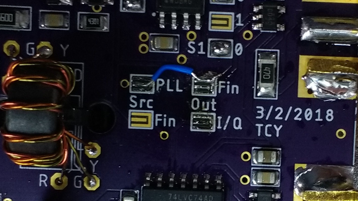
03/21/2018 at 00:33 • 2 commentsI finally got around to reworking the PCB to route the 4x PLL directly to one of the output drivers. It only took a few mm of wire and a steady hand.
![]()
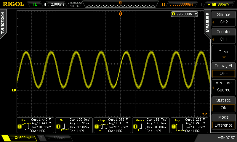
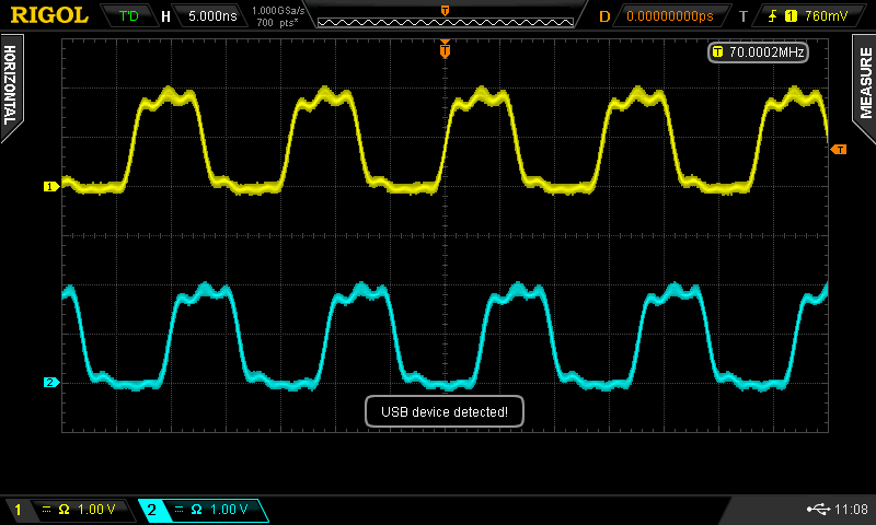
With this mod, the input signal is buffered, the frequency is multiplied by 4, and the result output on one of the ports. I cranked the TG frequency up until the PLL stopped following at 4x (at that point the PLL's VCO just stuck). The highest controllable frequency I was able to get was 296 MHz, shown here on a 300 MHz scope:
![]()
That's what you get when you look at a signal near the scope's bandwidth - everything looks like a sine wave, since none of the harmonics make it through. The input frequency from the tracking generator was 74 MHz (=296/4).
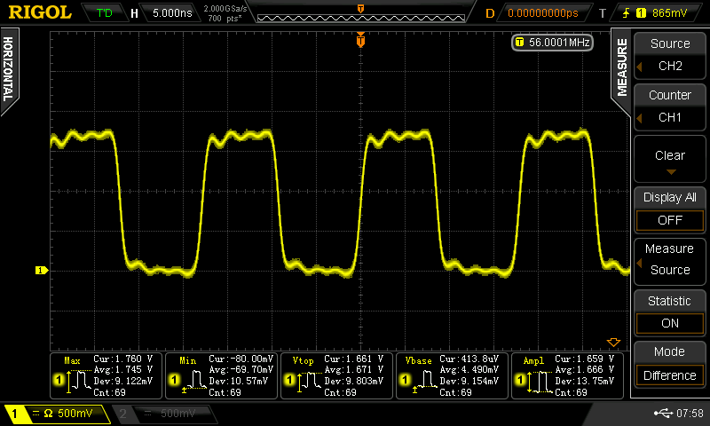
With lower frequencies, the scope can render the true shape more accurately, as shown here for 56 MHz (14 MHz input).
![]()
I think based on this experiment, I won't re-spin the board. I have 3 copies of the PCB from OSH Park, so I'll make one of them for I/Q outputs up to 70 MHz, one of them for a single clock up to 296 MHz, and maybe one that skips the PLL to go below 300 kHz.
A DC-296 MHz logic clock will do for the immediate future. That ECL is looking pretty good, though...
-
Debugging
03/18/2018 at 16:32 • 0 commentsI spent a little quality time at the bench this morning, trying to diagnose the issues with the first prototype board. The first find took much longer than it should have. I was poking around hopelessly at the front end with the oscilloscope when I realized I had a spectrum analyzer in front of me!
![]()
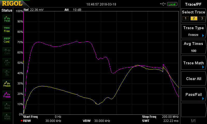
To capture these traces, I plugged a 10:1 oscilloscope probe into the input of the SA. This is always a little scary since the SA input is a bit delicate, but I was very careful. The vertical is set to linear mode to show the problems more clearly. The yellow trace is the signal right at the input jack, while the magenta is after the transformer (across R1), shown here for reference:
![]()
The difference in levels between the two is in part due to the transformer boosting the voltage. But, the shape of the traces shows the real problem. Although the input level drops off slightly up to 90 MHz, it picks back up afterwards, becoming very large between 140 and 160 MHz. I think this is due to reflection from the transformer performing poorly at these frequencies. The magenta trace tells a similar story. The magnitude drops off precipitously between 90 and 100 MHz, right where the input stage stops working.
I think the first thing to try is a different input transformer. I have a box of various cores I can try. Transformers on this core have worked very well for me in the past, but that has all been in the HF range or 50 MHz. It's interesting to see the limits.
I also suspect the protection diodes. They add a decent amount of capacitance, which could be an issue. Now that I think about it, removing the diodes (a single package) is easier than swapping the transformer, so I'll try that first. I'm not even sure I need the diodes with the 560-ohm termination there.
I also have a bunch of MSA0486 MMICs I could use for a preamp stage on a next PCB spin. They're almost perfectly suited to this application: DC - 3 GHz, with 8dB nominal gain and a +12 dBm P1dB. The only problem is the power supply. They need 5V at 50 mA, which has to be regulated with a resistor from a higher supply (at least a few volts higher). The easiest way to do this would be to bring 12V onto the board from somewhere, but it's kind of a big change.
While I'm thinking about next spins, there are a bunch of ECL flip-flops that could easily generate the I/Q outputs up to the maximum 1.5 GHz output of the tracking generator. ECL is a little bit of a pain to work with, but it might be interesting to make a version of this board that would go that high. I'd probably learn a whole bunch of stuff.
Output Source Terminations
I didn't have any 43-Ohm 1206 resistors, but I had some 39's. I swapped those out for the 27's I had originally to try to make a better match to 50-Ohms. The output swing went from 2.0V to 1.8V into a 50-ohm termination. A little more algebra shows that the output impedance is now 41.6 Ohms, so I should use a 47-ohm resistor instead. The 39s I had are only 5% tolerance, so this isn't exact, but It looks like it's converging. I do have some 47-Ohm 5%'s I can try on there next. They're easy enough to swap out.
Power Supply
I did a quick search on DigiKey this morning, and there a number of 3.3V regulators in the SOT89 package with current limits up to 800 mA (although 200 seems more common). Either would do for the approximately 150 mA maximum I'm seeing on the board. I need to re-check the power dissipation and make sure heat won't be an issue, though.
-
First PCB Assembled
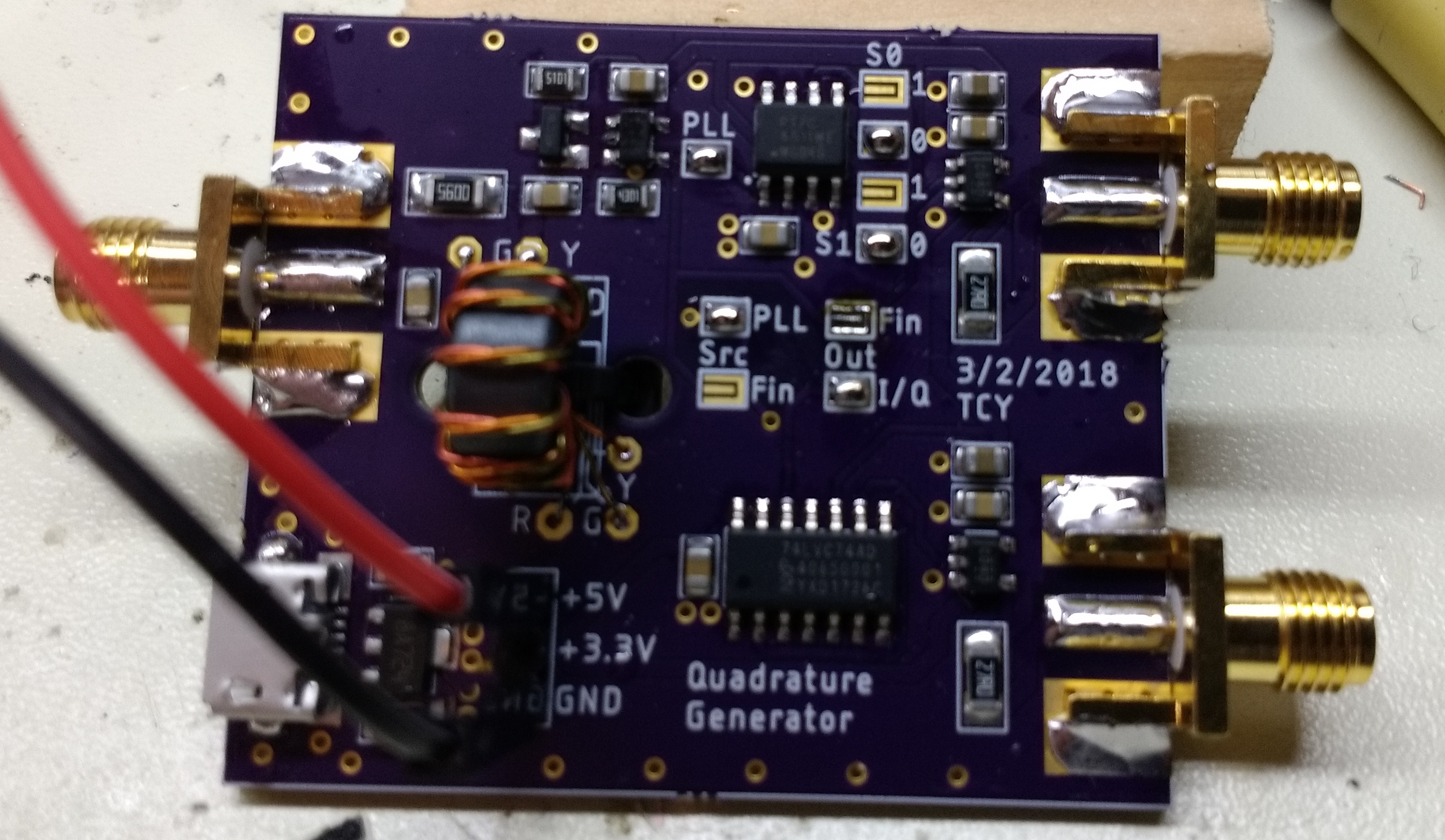
03/18/2018 at 04:25 • 0 commentsI found some time to populate one of the the PCBs this evening. The only problem was forgetting to put the USB jack on there before putting it on the skillet. I realized just as the first flux fumes were rising off the board, so pulled it back off to place the jack.
![]()
You can see the trifilar-wound input transformer on the left. I originally planned to load 10 turns of wire on the core, but only 8 would fit comfortably. I thought this might affect the low-end response, but it didn't (see below). You can also see the solder-blob programming sites I used instead of zero-ohm jumpers (or DIP headers) to configure the circuit. These worked better than I expected. To short one, you just melt a blob of solder on it, and you can open it back up with solder wick. Very easy to do. You can see them in various states here:
![]()
I wouldn't use them for sensitive analog stuff, but for digital lines, they're fine. The one thing I would change is to add thermals when the outer terminal is at ground. I usually don't do thermal reliefs on SMT boards, but the ones surrounded by the ground plane were a little more difficult to solder.
Testing
I tested the PCB by connecting the outputs to a 300 MHz oscilloscope.
Input Buffer
I first hooked the board up so that the output from the input buffer (a 74LVC1G14) was passed directly to one of the output drivers (a 74LVC1G04) so I could test the frequency range. I drove the input from the tracking generator of the DSA815-TG set in zero-span mode. At 1 MHz, the input buffer toggled down to -7 dBm input level, but the waveform symmetry was best above -4 dBm. On the high end, the input buffer was good to 93 MHz when driven at 0 dBm, the maximum output of the tracking generator. I honestly expected this to go higher. When I get a chance, I'll have to dig into it a little bit more.
Quadrature Generation
In this configuration, the input buffer feeds a 4x PLL clock multiplier, then the quadrupled frequency drives a quadrature clock generator made from a 74LVC74 dual flip-flop. Because the I/Q generator divides the frequency by 4, this configuration yields in-phase and quadrature clocks at the same frequency as the input. This mode worked better than expected. Here's the quadrature outputs at 300 kHz, about as low as it will go reliably when driven with 0 dBm input:
![]()
At this frequency, you can start to see a little jitter on the edges. It will actually toggle at lower frequencies, but the jitter becomes progressively worse.
The output is 2V p-p into a 50 ohm load (the scope has a 50-ohm termination mode). That's +13 dBm.
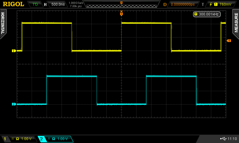
On the high end, it seems to work reliably up to around 70 MHz, shown here:
![]()
It's only a 300 MHz scope, so looking at the shape of 70 MHz square waves isn't absolutely precise, but they don't look bad. A very odd thing happens above 70 MHz - you can turn the input up to around 90 MHz, but the output sticks at 70 MHz! What's happening is that the PLL's VCO is maxed out at 280 MHz (70x4). That's still very good, since the PT7C4511 is only guaranteed to 180 MHz at 3.3V (200 at 5V). So, you can't count on this performance if you build one, but you might get it. Still, I expected to see a maximum of around 50 MHz at the I/Q outputs, so I'm pretty satisfied.
What this means, though, is that the PLL and the 74LVC74 are both running at 280 MHz. If I wanted a very fast clock, I could just wire one of the output drivers to the PLL output. Unfortunately, I didn't think of this when I designed the PCB. If I make another revision, it's definitely something to add. In the mean time, I still have 2 blank PCBs I could rework to try this out.
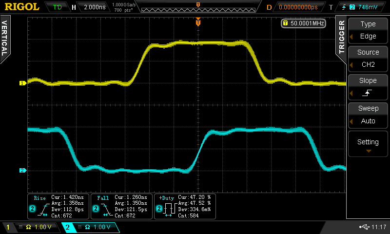
I measured the rise and fall time of the output clocks at around 1.35 ns, which is about the rise-time of this scope, so the outputs may be faster.
![]()
That's pretty fast, so terminated lines are required for any substantial cable runs, which brings up a problem I didn't see at first.
The outputs are source-terminated with 27-ohm resistors, which I thought would make 50 with the output impedance of the 74LVC1G04s. If this were true, the output peak voltage should be 3.3/2 = 1.65V. Since the output peak voltage is 2.0V, it means the 27-ohm resistors are too small. A little algebra (I won't bore you) shows the output impedance of the drivers plus resistors must be 32.5 Ohms, and the drivers themselves must be 5.5 ohms. This is much lower than I expected. Based on this, I'd need 44.5-Ohm resistors in the output to get a good 50-ohm termination. They make 44.2-ohm 1% resistors, and I probably have some 43-ohm 5% ones around to test. When I get a chance, I'll have to swap them out and see how the output looks.
Power Consumption
I had hoped the circuit would draw less than 100 mA so that it could be run off any USB port. At 1 MHz, I measured 78 mA from the 5V supply, but this rose to 144 mA at 70 MHz. The original idea was to power the PCB from the USB jack on the front of the DSA815. Now, I'm not so sure. 144 mA is definitely out of the USB specification. Maybe I'll use a USB current meter and plug something in there that requests more than 100 mA. If the request is granted, I can assume the DSA815 is capable of supplying that much. I'll have to experiment a bit. I can always power then thing from any one of a dozen USB power supplies around here, too.
Unfortunately, this also means that the 78L33 I'm using to create the 3.3V supply from the 5V input is being abused. It's only rated for 100 mA output. It didn't burn my finger during testing, but this probably isn't a good thing to do long-term. The PCB has a 3-pin header for GND, +3.3 and +5 volts, so I could power it from an external 3.3V supply until I figure out exactly what to do.
Overall, I'm pretty happy with this as a first version. It's definitely usable as-as, although I'd like to get that 280 MHz maximum output frequency working. That would probably be all I would ever need in a lab clock generator. Even as it is, the 70 MHz outputs greatly exceed what I could do with a 25MHz DDS which I was using before.
-
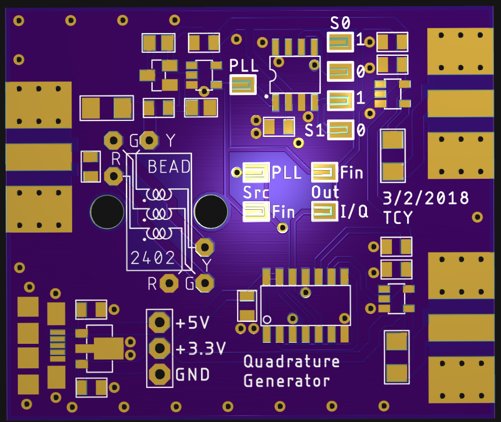
First Design
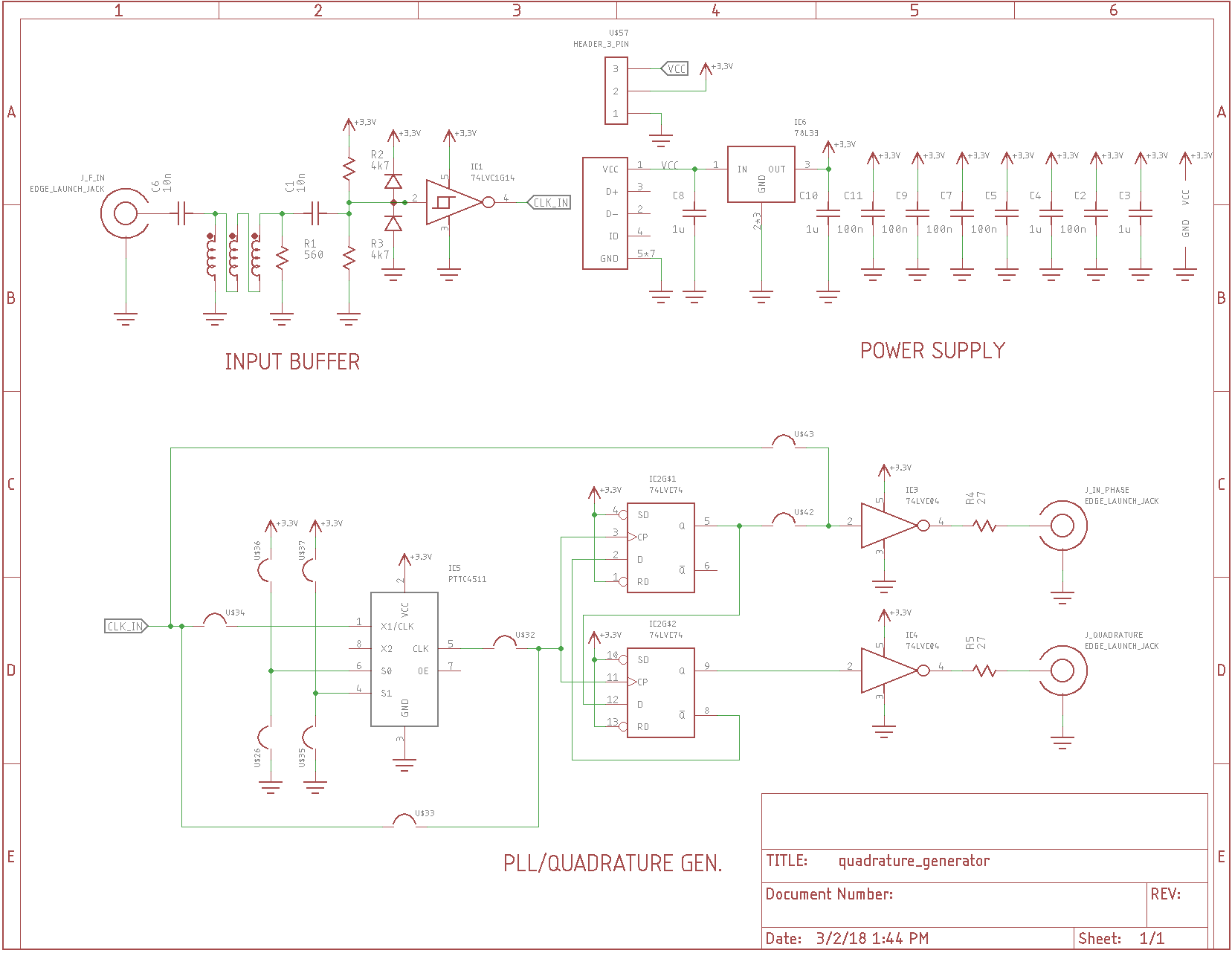
03/02/2018 at 19:15 • 3 commentsHere's the first design I just sent to OSH Park.
![]()
Input
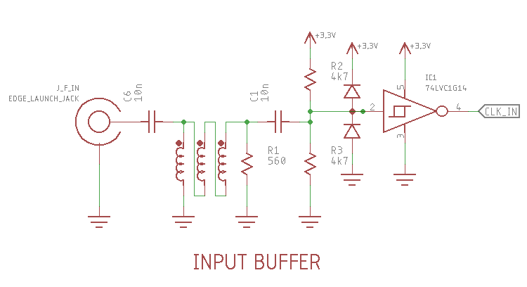
The input jack connects to the tracking generator output of the DSA815. This output has a maximum level of 0 dBm, or about 632 mV peak-peak into 50 ohms. I threw together a quick circuit to transform the 50-ohm input impedance up to 450 and boost the voltage up enough to toggle a 74LVC1G14 Schmitt-trigger inverter. To check things out, I simulated the front-end in LTspice XVII. Here's the schematic (note that the component designators don't match the schematic above):
![]()
The input is assumed to have a 50-ohm impedance. C3 is included just in case I decide to drive this board from some source with a DC offset (like another clock signal). As a first guess, the transformer is 10 turns trifilar wound #28 Ga wire on a Fair-Rite 2643002402 core (43 ferrite material). It's sold cheap as a noise suppression core, but the electrons don't know this. Hams can substitute an FT37-43. I'll have to see how this core performs at 100 MHz and beyond. A different core material might be better.
The 1:3 turns ratio transforms the impedance up to 450 ohms, which is terminated with the three resistors in parallel. The 5.1k and 4.3k resistors bias the inverter input half-way in between the worst case high- and low-going input thresholds (1.5V). The dual diode protects the inverter input from ESD. These diodes are optional - they may not really be needed, and do alter the performance a little bit. The 4.5 pF capacitor represents the typical input of a 74LVC1G14 inverter.
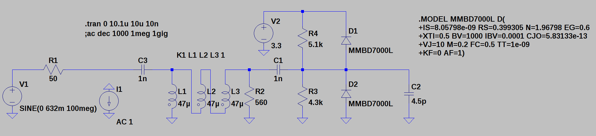
I ran a transient simulation at 100 MHz. Note that the amplitude of the input voltage source (before back-termination) is 632 mV p-p, since it delivers 0 dBm into 50 ohms.
![]()
The output has peaks about 2.25V, and troughs of around 0.8V. The 74LVC1G14 isn't spec'd at 3.3V, but from the 3.0 and 4.5V specs, I estimate the worst case positive-going threshold to be 2.04V, and the negative-going, 0.95V. Just on the edge, really. At 10 MHz, the peaks are 0.6V and 2.4V, which looks better. Of course, the transformer simulation is very rough, so this is little more than an informed guess at this point.
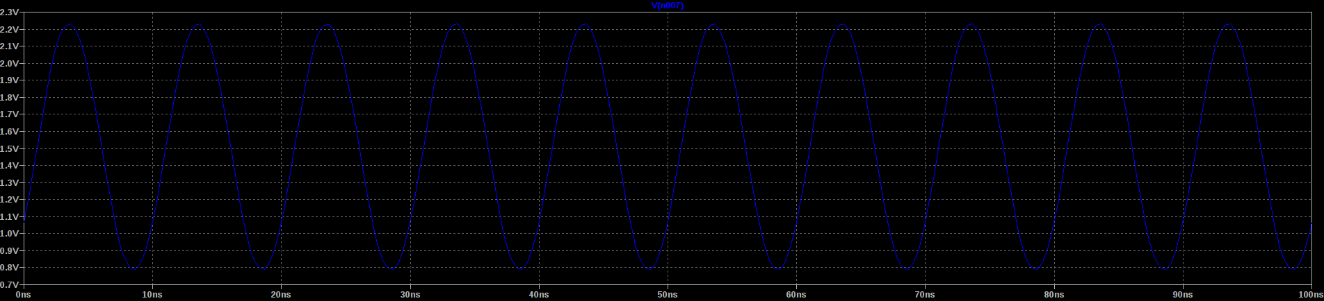
Input Match
I also looked at the input impedance of the simulated circuit. You can see here that the input VSWR is 2:1 or less from around 1.8 MHz to 117 MHz.
![]()
This is even more of a guess than the transient analysis above. It will be interesting to measure the input return loss of the assembled board and see how close it came.
PLL
I added a clock-mulitplying PLL on the board for three reasons. First, I'm not sure how fast the front-end will go, and the PLL provides the option of a faster output clock than the input. I also wanted to be able to generate I and Q outputs at the same frequency as the input, which requires a 4x PLL. Finally, I just wanted to play with this particular PLL. It's a PT7C4511 from Diodes, Inc (was Pericom). It can output frequencies up to 200 MHz with 9 different multipliers, in this case, selected with solder bridges on the PCB.
Quadrature Generator
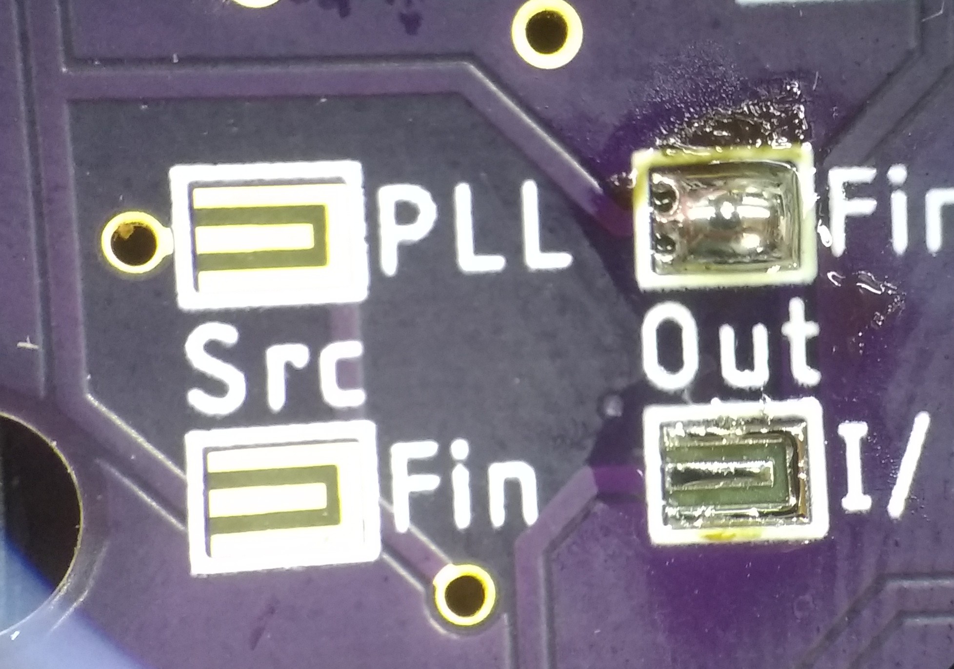
I used the classic Johnson-counter quadrature clock generator with a 74LVC74. It's supposedly good up to 200 MHz. There are solder bridges on the PCB for driving the clock from the input frequency or the PLL output.
Outputs
The I and Q outputs are driven from 74LVC1G04 inverters. The outputs are back-terminated with 27-ohm resistors, which I think will make 50 combined with the output impedance of the gates. I'll have to test this once the boards come back.
Power Ssupply
I added a micro-USB connector and 3.3V regulator as a power supply. The DSA815 has a USB port on the front which could be used for power (if I trust my PCB). Any USB supply should work. I also added header pins for 5/3.3V input or output.
Solder Bridges
I've used zero-ohm jumper resistors for board configuration before, but thought I'd try the cheaper solder-blob method this time. I made an Eagle component for this, and I can't wait to see how it works.
![]()
You should be able to blob some solder on there to close the "switch," or turn it off with some desoldering braid.
I sent the design off to OSH Park, so now I just have to order parts and wait for everything to arrive.
![]()
DSA815-TG Quadrature Clock Generator
An adapter to generate I/Q clocks from the TG output of the DSA815 spectrum analyzer