-
Intermittent Hardware Problems
07/09/2018 at 18:03 • 2 commentsThe intermittent hardware problem became obvious when I finally had the bootloader caused "bricking" issue resolved.
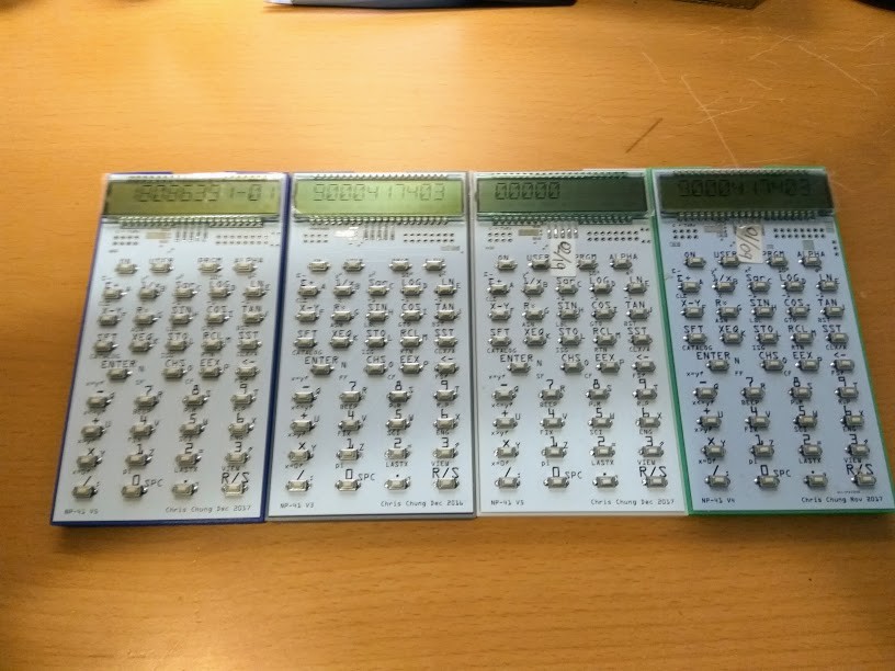
This is my first project that involves a LQFP device w/ 0.5mm pitch. When I was prototyping the project with the initial PCB designs, I had trouble hand soldering the MCU. After some research on the web, I tried and explored different methods, including stencil mask, baking it in an oven, etc. It took me about 6 or 7 PCBs and a few toasted MCUs I finally settled on a drag soldering method, which gives better and more consistent results.
Visually inspected solidly soldered boards still failed (not all) intermittently after use, typically this can happen after a few days to a few weeks. Most of them can be repaired via solder re-flow and sometimes a replacement PCB.

I had gone through 6 or 7 versions of PCB, and although there are improvements after working on trace length / size and ground planes, I still cannot eliminate this intermittent hardware failure. Unlike the bootloader problem which makes the calculator fails while executing, the hardware failure is more straightforward in that the calculator will refuse to start, or the charge pump will fail to attain LCD voltage, in turn fails the LCD display.
As a hobby level project, there is not much I can do except to do my trials and errors. I did tried and included troubleshooting code (like watchdog timer use) that the MCU can provide and can sometimes sees how things failed from the MCU perspective, the originating cause, however, is hard to trace.
The fact that the problem is intermittent suggested that it may be environmental. Did they fail more when the weather is dry? Or near a washer or dryer when they start to operate? How is ESD affecting the unit? I recalled the times when I was working in retail, seeing POS machines resetting themselves when a nearby ice cream fridge had it's condenser started spinning.
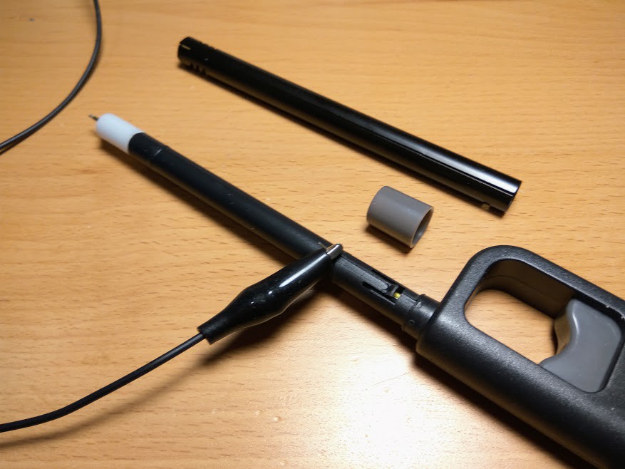
As a hobby level lab (and one without an O-scope), we improvised. I built this EMC testing rig from a $1 BBQ lighter. This particular lighter is easy to modify. After removing a sleeve and ring there is already a ground lead exposed.

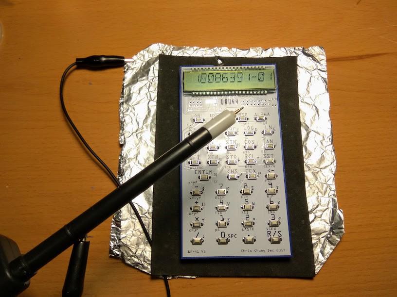
I would just need to use alligator clips to attach it to my ground which is a fold of aluminium foil where I would place the test unit on top. I would fire the lighter at a distance from the calculator and observe. When close enough the calculator under test would reset itself.

When I started to perform this test, I already had 5 different PCB designs.
By measuring the distances between the lighter and the calculator of different designs I can decide which design is more robust against ESD. I then focused on the best design and build multiple units.
The best PCB design improved the situation but did not eliminate the intermittent fails. Other facts from the ESD testing includes;
- I can improve the ESD tolerance by adding ground shield (aluminium foil) to the simple 3D printed case.
- If I fire ESD close enough and fire successively, I can kill a MCU.
I had since somehow concluded that this is caused by my soldering process and there is not much I can do about it.
As a hobby project, I am satisfied and happy with my results. I still have a few working units that I built and the oldest unit had been working for 2 years on the same battery. I used the calculator whenever I need to and sometimes will play with the programming and they are all fine for this purpose. It is fine because I created the project and if there are little glitches (button failed, segment missing due to cold solder), I can fixed that in one minute. Even if the unit failed to start, I will be able to fix it by re-flowing the MCU. This (the quality of the project) is not unlike many projects I created before.
For a kit project offering, this is very different though. I can give away these for my friends and if they failed next month, I could take them back and have them fixed. And when you sold these over the world (for my NP-25 project, I sent 100+ units to at least 15 countries), having them fixed is not that easy and economical. As I had mentioned in the comments section, my first batch of 10 units offered had 6+ units returned for repairs. It does no good to my customer and myself when they are these unreliable. So I had suspended offering them until I can reach a completely robust solution.
With the conclusion (I hope it is correct) that the problem lies on my manufacturing skills, the next logical step is to have it soldered professionally. And this is what I intended to do next. This may cost more and involve more logistics (parts, firmware flashing, shipping etc), but I think it is necessary if the project is to be offered as a product / half-kit.
-
Small Batch Production Trial
07/05/2018 at 18:36 • 0 commentsIt had been quite a while since my last project log. I had worked on the project on and off for the last 2 years.
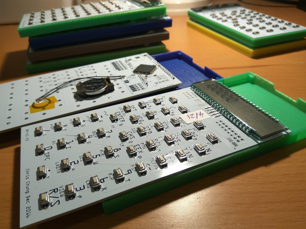
After successfully built the two-part prototype unit. My target was to create a design that allows me to offer the project as a DIY kit. And the two pcb design although works, is not ideal for DIYers. The headers need to be bent and it takes time to get the alignment right. I simplified the design into a single PCB to allow for easier assembly.

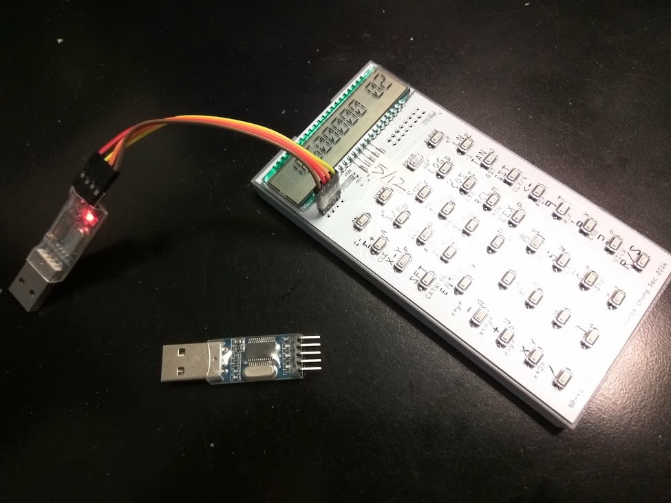
A buzzer had been added, along with an experimental application ROM support feature via USB-TTL upload.

I had also design a very simple case to house the PCB. A number of units were created in hope of that I can offer them for those who are interested. The units are hand soldered and after a few failures my skill was getting better and I had produced a dozen or so working units. Since the units were not reliable and did have intermittent failures, I held on to these for 5 or 6 months before finally offered them for sale. During which I would turn them on and off every few days and do simple operations to ensure their reliability, or so I thought.

10 units were sold and 6 of them were either DOA or failed after a few uses. I was not expecting this and it was a real set-back for my intention to provide the project as a hobby kit.
After retrieving some of the failed units I found that I can revive most of them by flashing the firmware again. I then spent time to reproduce this "bricking" problem and eventually found that the firmware was corrupted if the supply voltage was not stable during the application of initial power. This actually happens when the battery was being inserted. It had not happened during my 6 months testing with these units as I never tried to change battery. It was the jiggling of the CR2032 into the coin cell housing that triggered the failure.
Still this was a mystery as according to specification of the MCU this should not have happened. Eventually I found out that the issue lies on a custom bootloader I created to allow for user firmware upgrade via a USB-TTL cable. In my bootloader code I had relocated the PUR (power on reset) interrupt vector to point to my bootloader code. In my bootloader code I would wait for USB-TTL connection signals and instructions to upload firmware, which includes code to write to MCU's FRAM memory. There were certain standard MCU peripheral initializations that I had to skip (code space, I don't even setup a stack in the bootloader). And the jiggling of the coin cell had created a series of resets, combined with the lack of proper MCU startup, had caused random memory corruption.
This problem was corrected after I spent a couple of months of investigation. I had since re-written a more robust bootloader and had this issue fixed.
But this was not the only problem, newly assembled and repaired units were still failing, not when batteries were inserted but after a few days or weeks usage. There was something on the hardware side, not properly designed PCB, poor assembly method and skill, combined with environmental EMI issues is another challenge this project faces. I shall dictate that to another project log update.
-
NP-41 Taking Shape
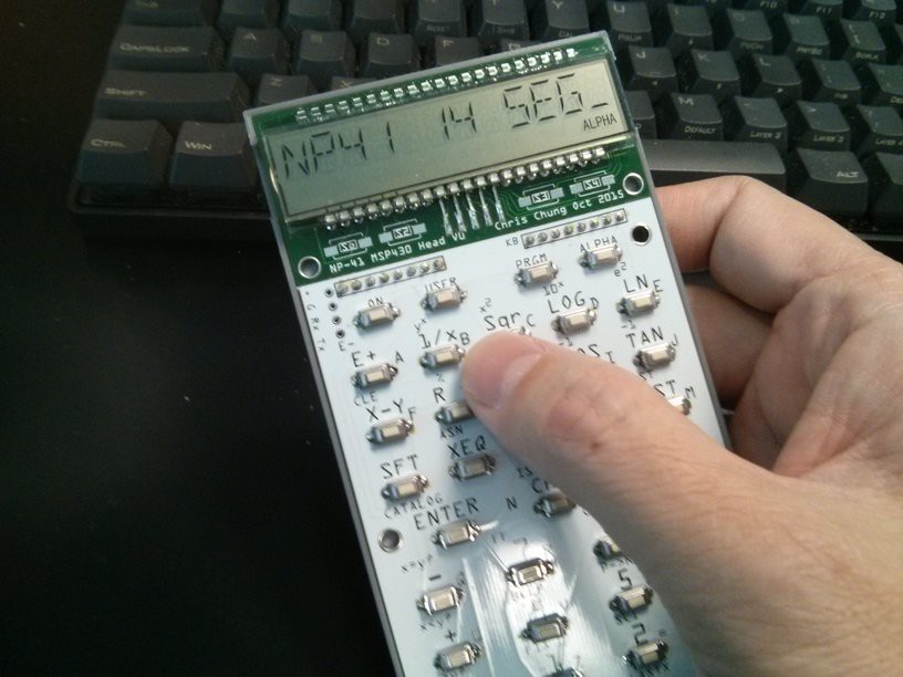
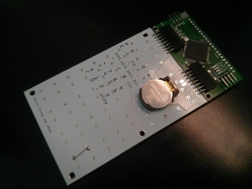
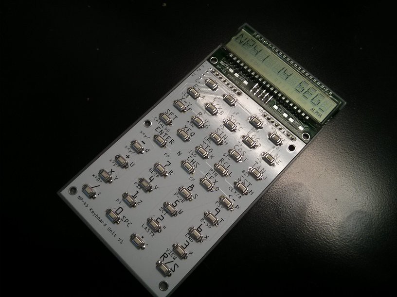
03/08/2016 at 16:15 • 1 commentThis is a new version of PCB design. There are actually two PCBs. The green head unit contains the LCD display and MCU. They keyboard part is in white PCB contains only the keys and the battery. This allows me to trial various keyboard designs.
They are connected via header pins as shown.
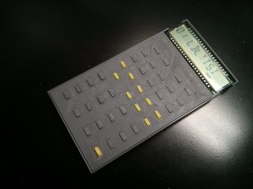
The whole unit "sinks" in a 3D printed case to allow for comfortable holding and operation.
There is also an experimental keytop structure w/ 3D printed keys. I do prefer the bare PCB instead, as I do not have means to print key legends and the 3D keys are coarse. I might try another 3D design in the future.
The calculator is basically operational. I am spending time to enhance the firmware. Mainly need to find ways to load extension modules. Will give updates in the future.
-
Engineering Unit #1
10/11/2015 at 23:25 • 0 commentsGot the keys working, will need more timing adjustment (scanning) as they are sometimes not very responsive.
I am running this on a partially depleted coin cell at around 2.85V. A 3V battery will produce too much ghosting on the LCD.
Will be designing a new PCB to move on. The charge pump still fails after 1/2 second. It drops to 1.66V instead of staying at 2.8V. I had tried different values and types of capacitors and still cannot get it to work. I had also ripped the capacitor pad off after excessive re-flows. Will include more options in a new PCB design for charge pump trials (also allows custom biasing to see if contrast can be improved.
Also found out that the current design w/ the use of a port 9, I cannot assign the "ON" key the role of h/w interrupt after getting into deep sleep. So the current unit does not have a good power saving sleep scheme.
I am just showing the video here as there is a lot of interest for it. My next PCB will just contain the MCU and LCD, plus a 9-10 pin connector to a keyboard. This will save cost at the current stage.
The final unit (for this PCB) is a bit large for my liking. I was indecisive when doing the LCD and had chose to match the HP-41C LCD size. It appears that based on that the product is more likely a desk unit (a slim one though) instead of a pocket unit. -
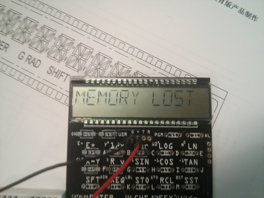
MEMORY LOST
10/06/2015 at 00:23 • 0 commentsThis is the first message you will see on a HP-41C calculator. Or when you replace your battery and have the internal memory reset.
I had assembled the a first prototyping unit. Took me two takes and a fired MSP430FR6989 MCU. I have not yet get the internal charge pump working so the LCD does not have the best contrast and have some ghosting issues.
This is an important step in this project as it's a proof of concept.
-
Custom made LCD Glass testing
10/01/2015 at 12:09 • 2 commentsI ordered custom made LCD glass for this project. They are about the same size of the original HP-41C display. It's a 14 segment display w/ 12 digits.
The LCD glass is made w/ 6 Mux and 1/3 bias. With 1/6 duty cycle the contrast is not the best but there are so many segments and my target controller for this project does not have enough segment pins for a 4 Mux.
I have not yet make this into a PCB so I am testing drive the LCDs w/ a test rig setup of GPIO direct driving the display. Resistor arrays are used to allow for setting proper bias voltages.
-
2015-08-19 Prototyping on TI LaunchPad
08/19/2015 at 17:36 • 0 commentsVideo showing a test run, 9, sin, cos, tan and back for forensic test.
And a "Cat 3" for internal functions. Some characters (like > and ?) was messed up and since fixed.
NP-41 RPN Calculator
NP-41 is a hardware realization of the Nonpariel calculator simulator. It executes the original HP-41C / CV byte-codes.
 Chris Chung