 Bruce Land
Keypad
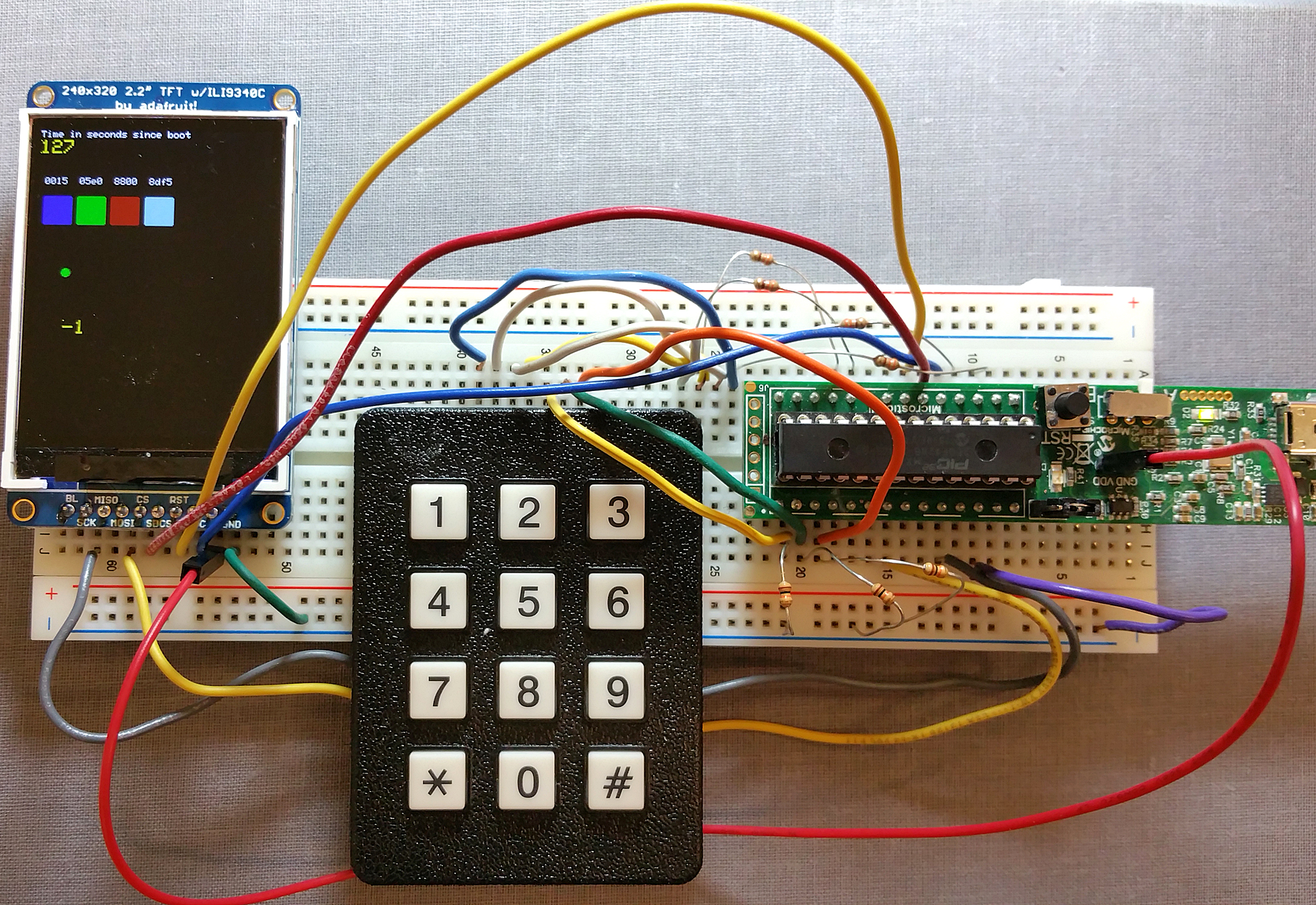
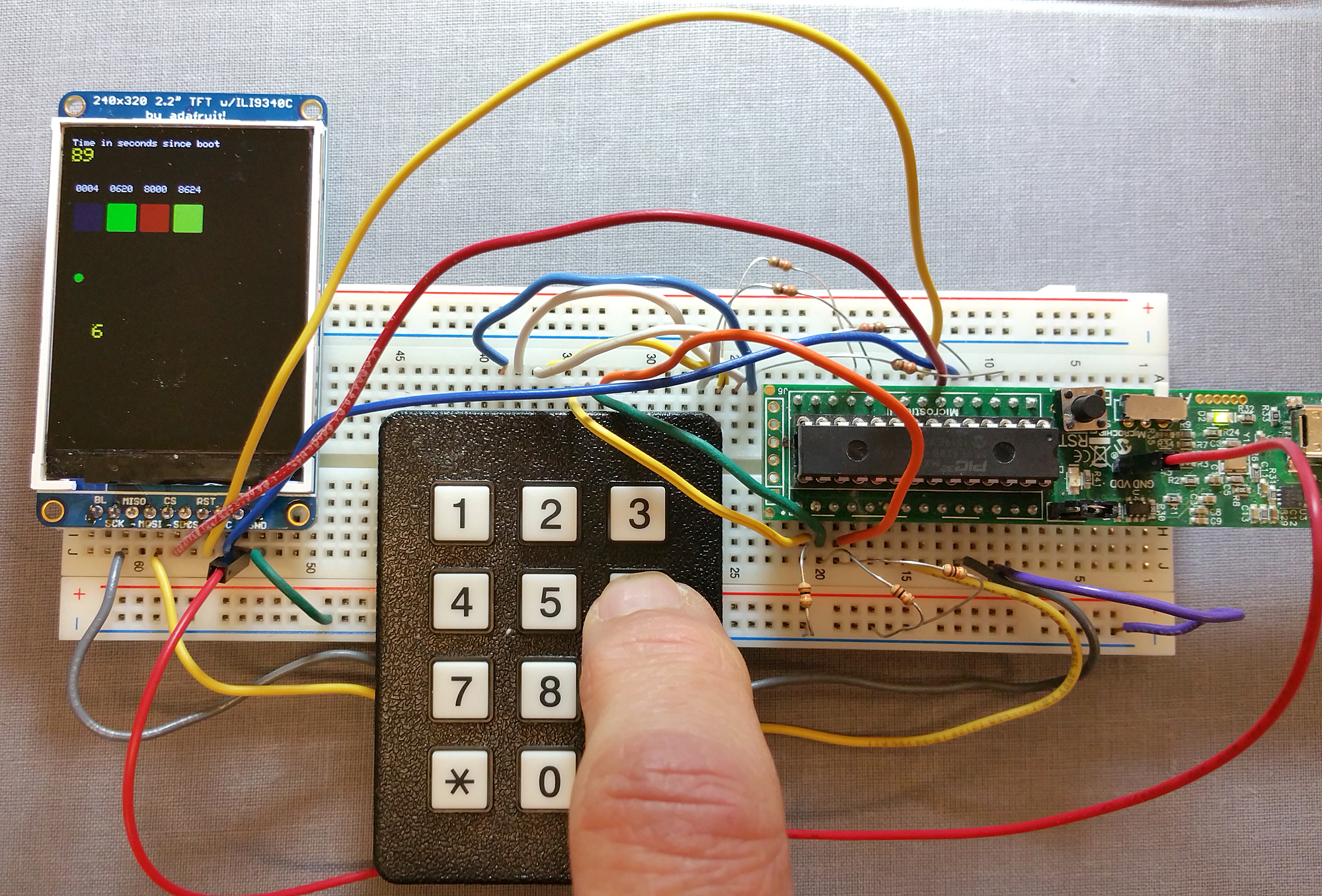
Adding a 12 key keypad (0 to 9 with * and #) requires seven i/o pins. Each switch connects one row wire to one column wire. Connection scheme used in the test code is shown below. 300 ohm resistors protect the outputs from short circuits when multiple switches are closed. The 10K pulldown resistors provide an input source when the switches are open. The code displays the button label when a button is pressed, and -1 when no button is pressed. If you add one line of code, you can eliminate the three 10k pulldown resistors by turning on internal pulldowns. The poorly documented CNPDB register (Change Notice Pull-down Enable B) selects input bits to pull down. Setting <br>CNPDB = BIT_7 | BIT_8 | BIT_9
in the keypad thread pulls down B7, B8, and B9. To be safe, you should probably clear the CNPUB register to turn off pull up resistors.
If you include the following macros:// PORT B<br>#define EnablePullDownB(bits) CNPUBCLR=bits; CNPDBSET=bits;<br>#define DisablePullDownB(bits) CNPDBCLR=bits;<br>#define EnablePullUpB(bits) CNPDBCLR=bits; CNPUBSET=bits;<br>#define DisablePullUpB(bits) CNPUBCLR=bits;<br>//PORT A<br>#define EnablePullDownA(bits) CNPUACLR=bits; CNPDASET=bits;<br>#define DisablePullDownA(bits) CNPDACLR=bits;<br>#define EnablePullUpA(bits) CNPDACLR=bits; CNPUASET=bits;<br>#define DisablePullUpA(bits) CNPUACLR=bits;
Then you can just write EnablePullDownB( BIT_7 | BIT_8 | BIT_9);
ZIP of project.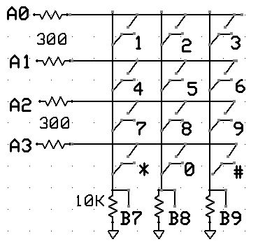
The physical connections for servral styles of keypad are shown below. You probably will want to use the
12-key models.

Connector:  top:8-pin      top:9-pin   bottom  12-key
Pin 1  ---- row 1 2 3 A    col 1       col 1    row 1 (pin A0)
Pin 2  ---- row 4 5 6 B    col 2       col 2    row 2 (pin A1)
Pin 3  ---- row 7 8 9 C    col 3       col 3    row 3 (pin A2)
Pin 4  ---- row * 0 # D    col 4       col 4    row 4 (pin A3)

Pin 5  ---- col 1 4 7 *    row 1       row 1    col 1 (pin B7)
Pin 6  ---- col 2 5 8 0    row 2       row 2    col 2 (pin B8)
Pin 7  ---- col 3 6 9 #    row 3       row 3    col 3 (pin B9)
Pin 8  ---- col A B C D    row 4       row 4    ----
Pin 9  ----              (NO CONNECT--common)

(a) Each switch shorts one row to one column. When in doubt, get the ohmmeter!
(b) On the 9-pin models, do not connect the common lead.
For DDS lab:
- TFT uses
pins 4,5,6, 22 and 25(RB0, RB1, RB2, MOSI1, SCLK1)
SCK1: connected to RB14 on the PIC
MOSI (SDO1): PPS output group 2 connected to RB11 on the PIC
CS: connected to RB1 on the PIC
SDCS: left unconnected as I'm not using the microSD card for this
RST: connected to RB2 on the PIC
D/C: connected to RB0 on the PIC
VIN: connected to 3.3V supply
GND: connected to gnd - DAC SPI channel 2 uses
SCK2pin 26
SDO2 (MOSI) is in PPS output group 2, could be connected to RB5 which ispin 14,but remember to set#pragma config JTAGEN = OFF, DEBUG = OFF<br>CS (chip select) connected to RB4,pin 12,but remember to set#pragma config JTAGEN = OFF, DEBUG = OFF - Keypad -- need 7 i/o lines (see schematic above)
A0 to A3 and B7 to B9

 Flo
Flo
 akash asbro
 jurc192
This kind of project takes me back to my own beginnings using microprocessors.
Back around 1980, I made a keyboard based on two 8-bit buffers driving the horizontal and vertical lines, with the buffers memory mapped into the address space of the CPU (6502). A more modern approach might be to use a latching shift register driven from just 2 i/o pins. An 8-bit register gives 4 lines in each of vertical and horizontal directions. I am not sure about the total time for the interrupt routine to read it, but it might be worth looking at to save some i/o pins if you need to.