For syncing the dimmer channels to the AC line, I put together a simple zero crossing detection and triac control in Diptrace. It's based on this design http://playground.arduino.cc/Main/ACPhaseControl but has some additional precautions like logic level MOSFETS, varistors and fuses. Also, I had to change some components for cost and availability reasons, the specs are pretty much the same. We're using high current 16 amps continuous load triacs here, so we won't have to cool them when driving 25 W bulbs.
Disclaimer: This is 230V AC mains circuitry, so if you want to do this, know what you do and don't hold me responsible for the outcome. It's dangerous, I strongly suggest that you don't build this by just copying the circuits if you're not able to figure it out by yourself. Take this content as purely inspirational, if not satirical! THX!
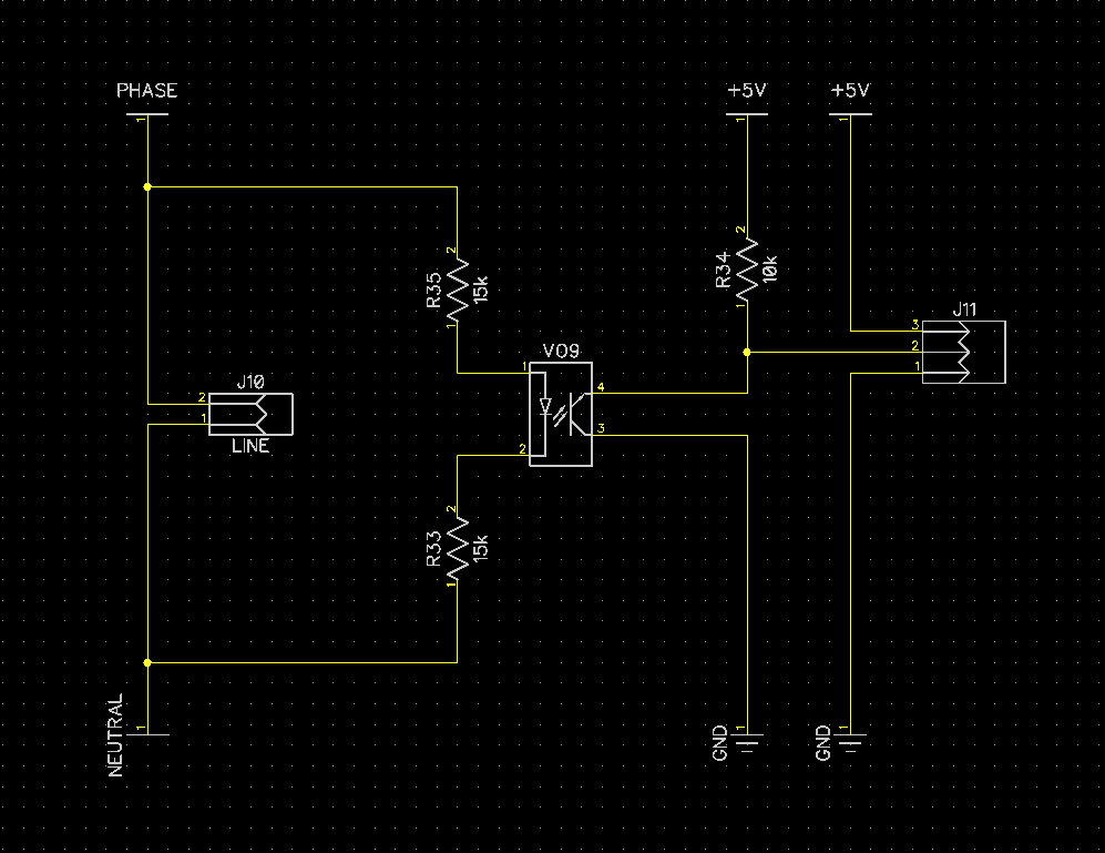
Here's the zero crossing detection circuit, I used a SFH620A AC-optocoulpler, which is pretty similar to the H11A11 from the arduino example:
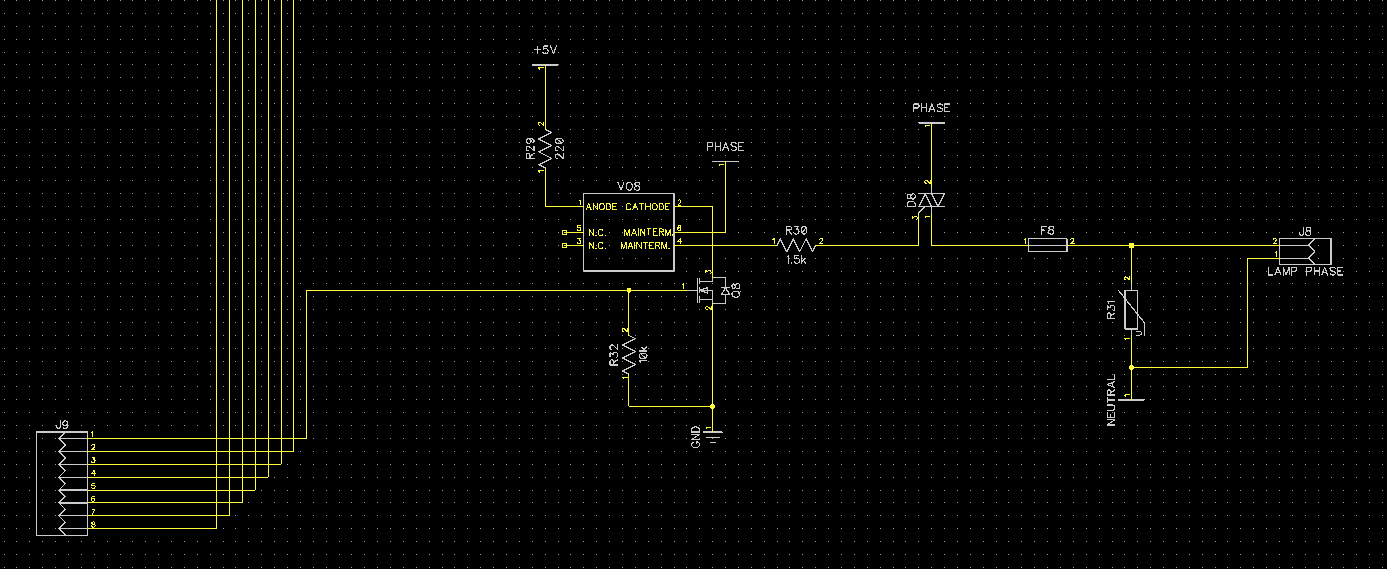
The triac driving circuit is based on powerful BT139 triacs (instead of the similar Q6015L5). Triacs are best driven by optotriacs, in this case the MOC3052-M. I will have 8 of those triac circuits and one zero crossing detection circuit on a 10x10cm pcb. Because I'm planning to drive many optotriacs, I cannot, or should not, power the optotriacs directly from any µC. The pulse, that drives the optotriacs cannot be neglectable short, so even if we're driving them at 15-25 mA, at some point, the forward current of all the optotriac emitters circuits would just sum up to something the µC cannot provide. Also, if the µC hangs, it might just blow. So I added thes nice little logic level N-MOSFETS, 2N7002, to every emitter cathode of the optotriacs. Almost any logic level N-MOSFET works here, use whatever you have. I've never had trouble driving logic level MOSFETS without gate resistor from any µC, but if you're worried you might as well add some. A pulldown however is necessary of course.
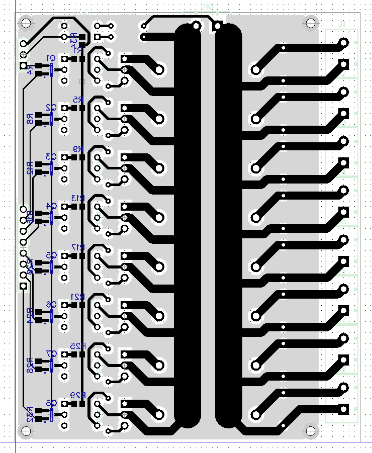
So, I've carefully tested everything on a breadboard, and even if these circuits are pretty basic, they seem to work reliable. However, there's a lot to improve. I.e. we should have some buffer capacitors and at least footprints for snubber circuitry for driving inductive loads, but one step after the other. I routed the boards single sided, so that you can easily fabricate them on a mill, but eventually, they will go to dirtypcbs.com, so the top layer has an optional grounded copper spill for shielding. The first boards will look like this:So, after some double checking on the gerber files, this went to dirtypcbs.com to get 10 nice boards. My plan is to use two of these boards for the lamp and 8 of them to make a 8x8 light bulb matrix. So, let's hope this works as planned.
In the comments esot.eric mentioned some worries about the earthed and grounded shielding copper spill covering both the logic part on the left and the mains half on the right of the PCB. He also investigated this deeper and posted some good information material that I want to integrate into this project log. He quotes his source like this:
"For each power supply stage, keep power ground and control ground
separately. Tie them together [If they are electrically connected] in
one point near DC output return of the given stage."
http://www.smps.us/layout.html
So, the mains part of the PCB should be spatially isolated from the logic part, which it is, but there's no good reason to cover the mains part of the PCB with a copper spill. First, this increases the risk of HV making it into the logic and damaging it, and second, this messes with the idea of shielding the logic part against EM irradiations of the high switching current transients. While this is definitely a design flaw that will be removed from the sources, I am not to worried about this causing too many problems in practice. The copper spill is grounded and will be earthed, so its still unlikely that failures in the mains part will damage the logic. Even if, it will defenitely blow the leakage current fuse and turn the lights out.
In further investigation, I also found an example implementation of a electronical controlled dimmer here, and it's clearly visible that the copper spill ends exactly between the HV and the logic side of the optotriacs.
 Moritz Walter


Discussions
Become a Hackaday.io Member
Create an account to leave a comment. Already have an account? Log In.
Thanks for looking into this, any advice on this is very much appreciated! This is designed for 230V btw, should add that to the docs.
The ground plane will be connected to the housing, logic GND and mains GND. I've seen this in many devices, especially power supplies. At least in theory this should do a good shielding job. It also makes sure the leakage current fuse in your breaker box blows if there's a short on the board.
I also thought about using a comparator or even a voltage divider with current clamps, but the thing with monitoring AC (i.e. from a transformer) is, that I actually don't really want it in my logic, even at 9V AC. There's always dirty peaks in there. But well, if it works, it works, right?
And yes, the 15 k's do get hot. Since they're in series there's about 8 mA running through them, burning away almost 0,9W on each one. For now I'm using 1W metal film resistors, but I think this is just not enough safety margin. I'll probably replace them with some TO-220 resistors + heatsink there.
Are you sure? yes | no
Definitely sounds like you've planned this out quite carefully! Thanks for the informational-foodstuff :)
Good call about isolating AC, further than even a transformer... hadn't considered the "ugly peak" / surge-factor, though I did have some sort of inkling of discomfort at doing it the way I did it as anything other than experimental/proof-of-concept, didn't really spend any effort on figuring out *why*.
I'll have to look into this PCB ground-plane thing, though... I could swear the vast-majority of power-supplies I've seen have 'em separated, maybe connected with a capacitor.
Are you sure? yes | no
Hum, if this ground plane thing really bothers you, I guess I also have to double check that again, also don't want any serious design flaws in mains circuitry. I'd also be very happy if you could share your findings about that here if you find out something. I think I've disassembled countless ATX power supplies and they all had their GND earthed + connected to the metal housing, I'm not particularly confident with the exact PCB layout of my ground plane since it's just a large copper spill. I also don't know if I'm adapting this to this application right...
Are you sure? yes | no
Sorry to harp on this... but you asked :)
I can't seem to find anything official/specific, and I'm certainly no expert on line-level circuitry. But there are some similarities in your design with an ATX power-supply... In that, they both have two distinct sections, one for low-voltage control signals, and the other for high-voltage/current... *Connecting* the low-voltage ground to the AC/earth ground is common-practice (depending on your circuit's needs). But actually having a copper-fill "ground-plane" on the PCB under 120/240 traces... AND having that same plane also going under low-voltage/control circuitry (the gray box in the lowest picture here, right?) that strikes me as questionable.
This is the best I've found so-far:
"For each power supply stage, keep power ground and control ground
separately. Tie them together [If they are electrically connected] in
one point near DC output return of the given stage."
http://www.smps.us/layout.html
In a sense, your circuit is similar to a switching power-supply; the sense that you want to isolate low-voltage "control" signals from the high-voltage/power signals.... note in this image that the line-level circuitry is distinctly separate from the low-voltage (though their Grounds are connected via the screw-mounts and the supply's housing):
There are no traces nor planes/spills between... e.g. with your opto-triacs, they have a distinct low-voltage side and high-voltage side... it's probably best to do like this image and keep it all separate. On that note, it may be wise to move those resistors and the 5V trace, as well, at least keep it as far away as possible from the line-voltage traces...
and I see you've already ordered the boards... so it's all moot :) It'll probably work.
Are you sure? yes | no
Hey man! Yes, I asked! Thanks for contributing this! I guess a half-wrong approach is wrong even if it's half right ;) As I understand this now, I totally agree that a copper spill underneath the mains part does not make much sense and should not be done. Unfortunately, since the PCBs are manufactured and equipped already, now I could only fix the remaining unequipped PCBs by milling out a V-groove manually, seperating the mains half from the logic interface half. However, even if it's not best practice, the presence of the copper spill does not cause bad trouble in practice (well, yet ;). As long as the copper spill is earthed properly, I might get away with it. Even if a trace conducting mains voltage would short to the plane it would just run to earth and blow the leakage current fuse, at no time there would be mains voltage reaching the logic. Well, but honestly, you pointed out a serious design flaw there so thank's a lot for that! I'll fix it in the sources which will be released once this is finished!
Are you sure? yes | no
Never did any 120V PCBs... Not sure if you considered whether there might be an issue with having a shared ground-plane under 120V and low-voltage circuitry... (possibly even with having a ground-plane under 120VAC at all, seeing as how it'd act like a capacitor?)
I used a 9VAC wall-wart and a voltage-divider into a zero-crossing comparator-input, and rectified/regulated the 9VAC for the circuitry. It seemed to work, but I'm not certain there's no phase-shift on a (loaded) transformer's output... and I certainly didn't go so far as to do gamma-correction ;)
I'm sure you considered this, but those 15k resistors caught my attention... always wondered why I saw so many neon-bulbs well into the LED era... Quick-calcs, it looks like those resistors need to handle nearly half a watt. Not so bad, though... in the early days of LEDs that current certainly would've been too dim to see; 20mA would be 2.4 Watts... now I get it!
Oh, and I just saw something about using zero-crossing to ease the strain on relays, kinda clever.
Are you sure? yes | no