 Yann Guidon / YGDES
-
1Step 1
First, build the DIP8 adapter.
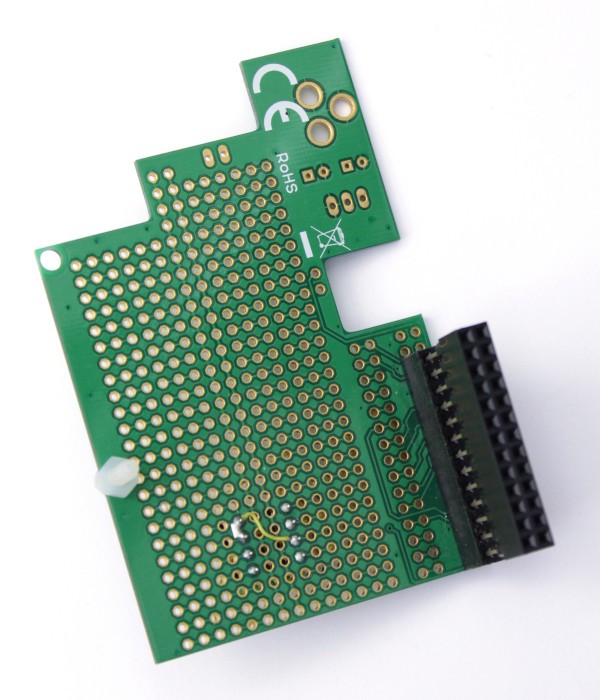
This is not a complex circuit, here is one I made for the Pi:
![]()
![]()
Required parts :
- PCB (a simple prototyping board is enough)
- some thin wire
- a female connector to plug on the Pi's extension bus (2×13 or 2×20 pins)
- a DIP-8 socket. Or a suitable ZIF socket.
- Not show above : the obligatory 100nF capacitor between GND and 3.3V supply close to the socket.
That's a few €/$ at most.
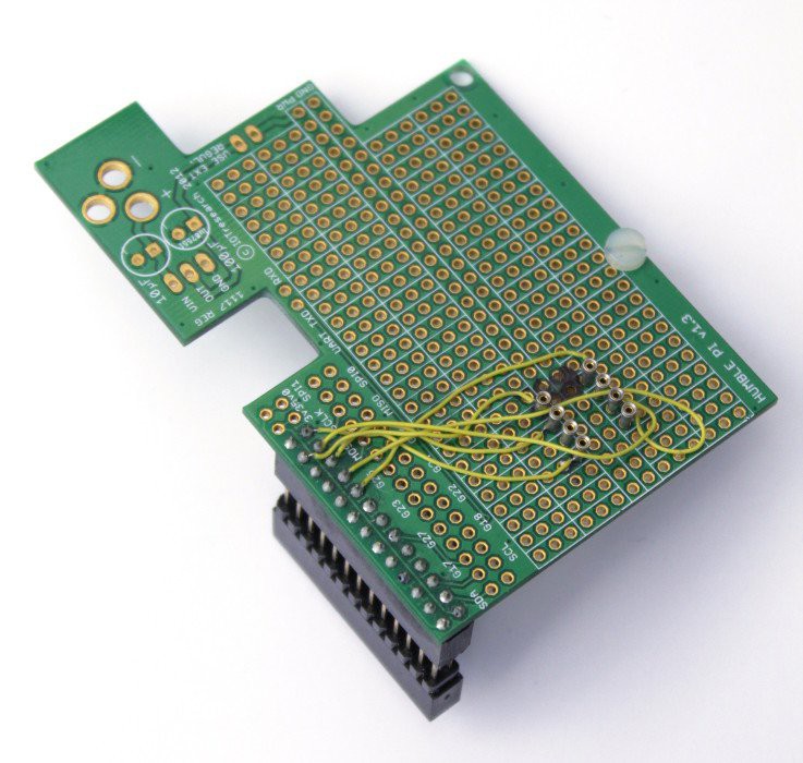
The soldering part is not hard : GND, 3.3V and 4 data signals:
![]()
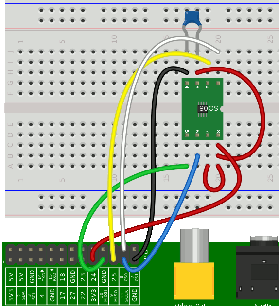
For the breadboard fans, here is the wiring:
![]()
-
2Step 2
The console.
OK I admit, I lied. This is not a SPI Flasher but a cog in a larger development environment. I designed this system to access the #WizYasep's "console port" so you can skip this part if you're not interested in cheap FPGA hacking (or the WizYasep).
My "production" flashing board has a HE10 header to help develop and debug configurable logic. I developped the following interface because existing JTAG debugging systems are proprietary, often expensive and not portable across vendors (my system works whether you're A, L, M or X).
This "console" port provides a slave SPI interface, a full-duplex asynchronous serial interface and an external RESET input (very handy). Another signal controls the function of the FPGA's pins : either user/design function (GPIO mode?) or "console" function (with SPI and serial data available, plus external control of /RESET). Of course, be careful to design a circuit that can still work when its GPIOs are not connected to the outside world ;-)
The SPI signals are further multiplexed inside the FPGA and the debugged design can also work as a SPI slave. The external RESET signal selects who gets the data: FPGA slave when high (normal operation, where the FPGA can also access the Flash to fetch data), or external SPI chip when low (bypass mode, signals are routed from a pin to another). This is "transparent" and irrelevant when there is no FPGA (directly connected to the SPI chip) or if the FPGA contains an empty design.
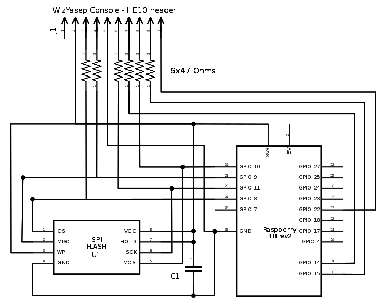
Here is the HE10 pinout :
- unused (yet)
- IO mode (0V=GPIO, 3.3V: console) (FPGA pulldown)
- RPi SPI Slave Select (0V: bypass to Flash, 3.3V: internal slave) (FPGA pulldown)
- RPi SPI MISO
- GND
- RPi SPI CLK (FPGA pulldown)
- RPi serial TxD (FPGA pulldown)
- RPi SPI MOSI (FPGA pulldown)
- RPi serial RxD
- RESET input (0V: normal FPGA operation, 3.3V: freeze the FPGA and SPI bypass) (FPGA pulldown) (yep this is inverted from the usual designs but for a good reason)
(note: all signals must be compatible with 3.3V CMOS ! They are also protected with a 47 Ohms resistor on the RPi side, in case the FPGA is in GPIO mode by accident)
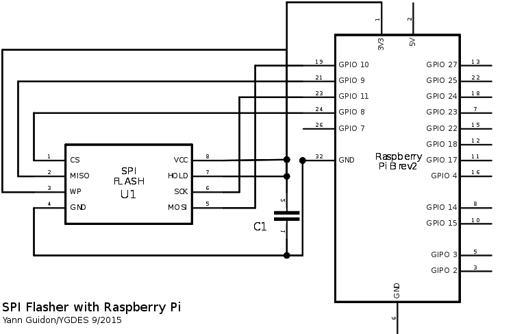
![]()
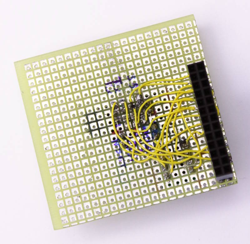
The RPi is connected to the HE10 header with the 4 SPI signals, the 2 serial signals and another GPIO (n°22) is required to toggle the RESET signal and enter into SPI bypass mode (RESET is set to 1 during programming, the FPGA design restarts immediately when it's done). The "IO Mode" signal is tied to 3.3V and fixed to console mode (unless you want to play with it). The other side of my everyday board looks like this :
![]()
There, you see, adding serial signals and a RESET output does not make a significant difference between the vanilla SPI Flash programmer and the more advanced FPGA debugger system... I keep the DIP8 socket on the board in case I need to test new parts or to check the RPi side is working correctly (in case of heisenbug).
-
3Step 3
Test the signals on the socket, to validate the wiring.
You wouldn't want the magic smoke to escape and render your circuit(s) useless! A short circuit or a mistake is so easy and devastating... Use a white LED tied to GND and to the desired signal (white LEDs easily stand 3.3V without a series resistor), or a multimeter, to check that all the pins are correctly connected.
First, check the signals as output. With a Python or bash script, make the following GPIO blink :
- GPIO8 should blink the SS signal (pin 1 of DIP8 and pin 3 of console)
- GPIO9 should blink the MISO signal (#2 of DIP8 and #4 of console)
- GPIO10 : MOSI signal (#5 of DIP8 and #8 of console)
- GPIO11 : SCK (#6 of DIP8 and console)
- GPIO14 : TxD (#7 of console)
- GPIO15 : RxD (#9 of console)
- GPIO22 : RESET (#10 of console)
Make sure to return each pin to "input" function after it is tested!
Bash scripts are provided there https://hackaday.io/project/17066-c-gpio-library-for-raspberry-pi/files or http://ygdes.com/sources/Pi/
- http://ygdes.com/sources/Pi/GPIO_on.sh sets a pin to 1
- http://ygdes.com/sources/Pi/GPIO_off.sh sets a pin to 0
- http://ygdes.com/sources/Pi/GPIO_in.sh sets the pin as input and reads the state.
Then connect a wire from the SCK pin (#6) of DIP8, to MOSI (#5 of DIP8). Turn SCK on and off and read the state of MOSI:
GPIO_on.sh 11
GPIO_in.sh 10
# --> "GPIO10 =1"
GPIO_off.sh 11
GPIO_in.sh 10
# --> "GPIO10 =0"
# return to input mode :
GPIO_in.sh 11
You can also tie RxD to TxD (loopback between GPIO14 and GPIO15) and send data to check that the HE10 connector is correctly wired. -
4Step 4
Check the features of the chip you want to read or program.
You can't avoid this : if your Flash chip is not in the supported list (most likely), then you have to find and examine the datasheet of your part.
Most of those parameters can not be automatically detected so you must be careful! At best, read or write will fail.
Locating the PDF is usually as easy as a Google search. Well, make sure the chip is the right version from the right manufacturer because parts evolve subtly over time, as fabrication moves to different foundries or bugs are fixed...
- Check the nominal supply voltage : is it compatible with 3.3V ?
Language such as "2.7V - 3.6V Supply" or "Vcc Power Supply" is OK, don't look at the "Absolute Maximum Ratings" which are extreme physical limits, not the operating range. - Speed (this is configurable in software, we use the "standard speed" not the "high speed" mode that is most likely advertised)
- Pinout (all 8-pin chips in DIP8, SOIC8 etc. use the same pinout but you are never too sure)
- Memory array structure : what are the block sizes ? Are the sizes uniform ?
- Does it use a standard 256 bytes write buffer ?
- Instructions : what commands does the chip understand ?
The basic instructions are standard but some manufacturers don't care...
The programming algorithm uses the following instructions :
- WRDI (0x04) : Write Disable
- RDSR (0x05) : Read Status Register
- WREN (0x06) : Write Enable
- READ (0x03) : READ Read Data Bytes (standard low speed, which is not easy to find in the datasheets, which quotes the "fast" speed of instruction 0x0B but the RPi is not used at full speed)
- RDID (0x9F) : Read IDentification
- RES (0xAB) : Release from sleep + Read signature
- BE (0xC7) : Bulk Erase : from 2s for a small chip to 40-200s for 128Mb !
The following necessary instruction are more tricky:
- PP (0x02) : Page Program
Suitable for AT26DF321, M25P40, 25LC1024, A25L40P, W25Q128F : 3 address bytes then 1 to 256 bytes to write. However the SST25VF032B/SST25VF016B accepts only 1 byte to write so it is not supported with this algo. - SE (0xD8) : Sector Erase (standard 64KB sector)
For A25L40, the sector size depends on the address ! (this is not handled). Some chips such as 25LC1024 have a different granularity so a different instruction must be used. - UPS (0x39) : Unprotect sector (Some chips like AT26DF321 are shipped protected so they must receive a first unlock procedure)
Please contribute to this list !
- Check the nominal supply voltage : is it compatible with 3.3V ?
-
5Step 5
Transcode your data to/from .HYX
HYX is a custom file format for this project. Documentation and filters are provided for raw binary and JSON formats.
It has a new project page there: #HYX file format
-
6Step 6
Download the source code and run the self-test scripts.
Currently the source code is at http://archives.yasep.org/yasep2014/C/
Download the whole directory and subdirectories (also contained in the .tgz) in a new directory on your Pi then run the test scripts in increasing order:
01_hyx2bin.sh
02_test_SPI_Flash.sh
03_read_SPI_Flash.sh
(etc.)
If all the scripts run without error, your system should work with the command-line tools !(to be continued)
-
7Step 7
Setup the Apache server and configure the CGI interface.
Command line is functional but not always handy, it can also work through a HTTP interface but more configuration work is required.
(to be continued)
-
8Step 8
Test the whole system with an example page.
(to be continued)
SPI Flasher
Got a Raspberry Pi ? A few more bucks turn it into a networked SPI Flash chip reader/writer
Discussions
Become a Hackaday.io Member
Create an account to leave a comment. Already have an account? Log In.