 Ian Hanschen
Some years ago, I set out to make my own OLEDs. This took a lot of persistence as many materials providers, manufacturers, and researchers refused to work with me, some of them providing their own brand of discouraging words along the way. Luckily, I was able to find several companies and people researching and working in the field who were very helpful.
Anatomy of an OLED
I was able to successfully make several differently-colored devices of varying quality level. In some cases I used indium as a cathode. Here’s what the successful stack I chose looks like:
ITO stands for indium-tin oxide. It is an oxide that results from sputtering from an indium-tin target – usually onto glass, making a piece of glass that is conductive, and yet still transparent. ITO glass is used in most modern display technologies, including both displays and the digitizers that overlay them.
The ITO at the top of the stack in this diagram is simply used as a sheet of glass to help seal off the device while allowing an electrical connection to the gan eutectic below it.
The gallium-indium-tin eutectic is used because material deposition equipment is expensive, so something that can easily be deposited at low heat must be used. In addition, when the cathode material is in immediate interface to a layer in which electron charge is to be favored (such as the emissive layer), the work function of the cathode is very important. It must have a lowered conductivity such that it favors electron injection in the interfacing layer. The combined eutectic has both of these properties. It oxidizes easily and can be a little messy, but is relatively easy to work with. Indium can be used instead, as it has a low melting point, but its work function is a little higher, which makes devices not as bright as less electron injection means there is not enough of the recombination in the stack happening in the emissive layer. In addition, it has a melting point of 156.6°C, which I’ve found can hurt the rest of the stack beneath the indium cathode. The eutectic is liquid at −19 °C which is WELL below room temperature, so no heat is required.
I had varying levels of success with several different emissive materials – apart from Alq3 (which didn’t dissolve well in Toluene), I was able to light them all up.
- Small molecule based emitters:
- Polymer based emitters:
On the other side of the emissive layer is the PEDOT:PSS layer. It services as a hole-only layer, blocking electrons, once again forcing more recombination to happen at the interfacing layer. The layers above and below an emitter are often made up of hole blocking/electron transport layers (which are inversely, electron transport/hole blocking layers), working together to ensure that the electron injection happens inside the emitter where radiative recombination is most desired.
Then the anode layer is another simple piece of ITO glass through which the light is emitted, completing the stack.
Any number of transport/blocking layers and emitters can be found in use in one stack. There are white OLEDs, that, for example, have red, green, and blue emitters in the stack.
Making my OLEDs
Click any image below to open the lightbox.
Please specify a Flickr ID for this gallery
Sources of help and equipment which were crucial to my work
State surplus:
– Fume hood
Home Depot:
– Ducting for the fume hood (remember, it’s only being used for a small amount of solvent, and some nitrogen gas from when the spin coater is running).
eBay:
– Fume hood motor/fan assy.
– Spin coater
– Autopipetters
– Hot plate
– Misc. lab supplies (stir bars, vials, autopipetter tips, etc.)
– Safety...
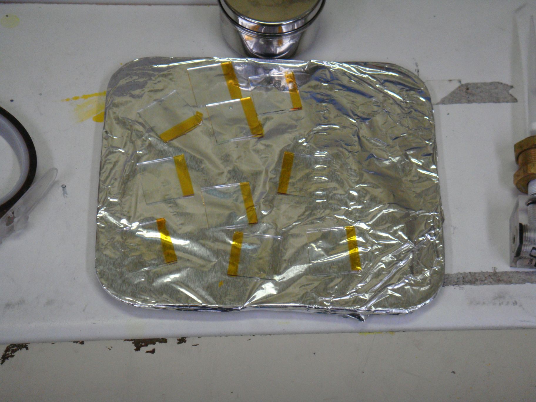 The first thing I do is take pieces of ITO (Indium-Tin Oxide) glass and figure out which side has the conductive coating. Then I apply a small piece of kapton tape to the edge. Each side will make up one cathode and one anode side for a given device. The kapton tape ensures both sides have an uncoated area for attaching an electrode to test the device.
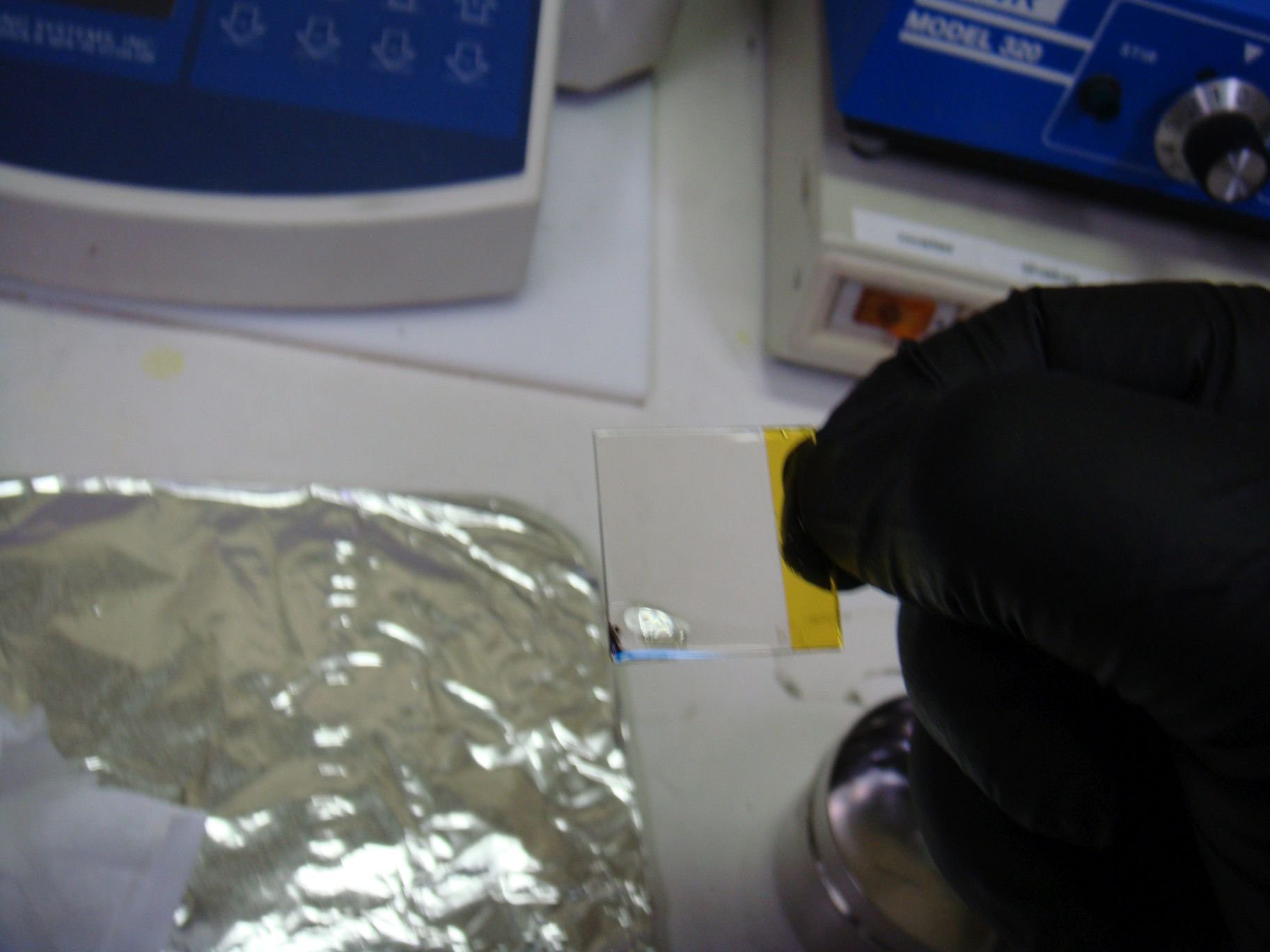 Each slide is then cleaned using solvent and dried off using nitrogen gas.
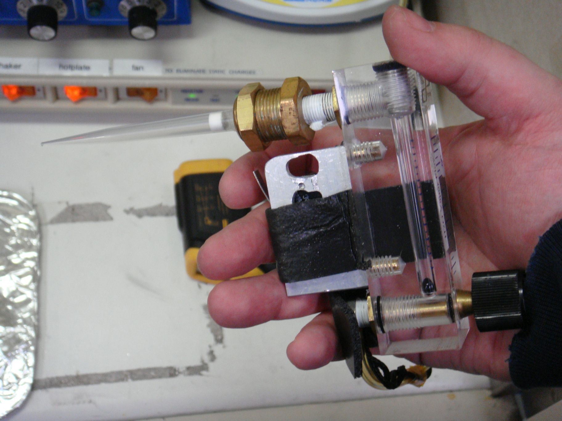 This is my nitrogen gas gun, done on the cheap. It was built using a filtered pipette tip, a gas flow limit/monitor, and a momentary switch attached to a solenoid (not pictured) on the gas line.


Nice project. I'm also excited to see the organic transistor you plan to make. Cheers!