 Yann Guidon / YGDES
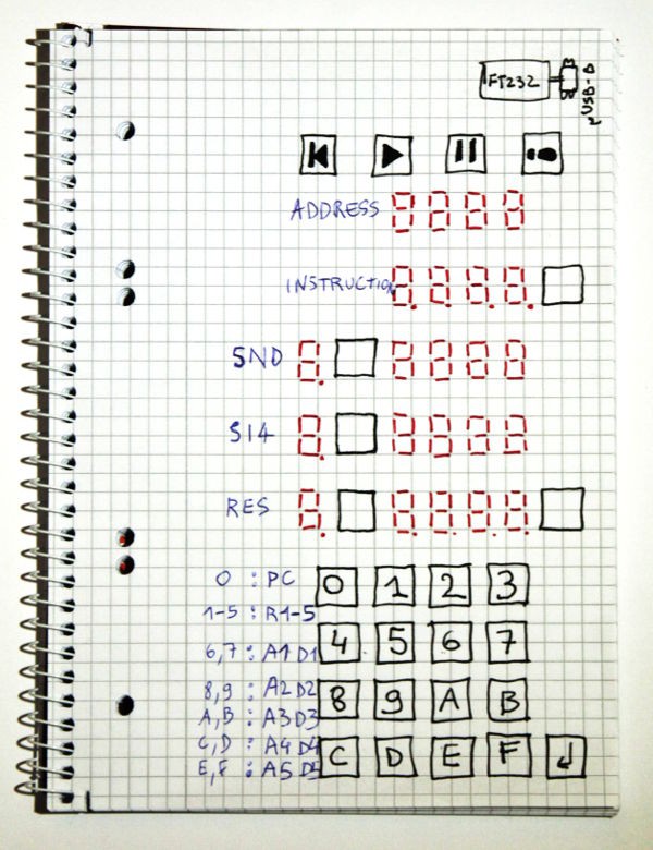
Now that I look at it, it feels oddly familiar... https://en.wikipedia.org/wiki/Apollo_Guidance_Computer ?
User Interface
Several HEX 7 segments displays show the current values on the busses and the current state of the processor.
Some values can be changed :
- press on the corresponding "select" button
- input the desired value on the hex keypad (the decimal dot will show which digit is about to change)
- press the "valid" button to update the value
- you can abort by re-selecting, or selecting a different field instead of validating.
You can examine the processor's contents by changing the address fields of SI4 and SND. The 16 listed registers can have side-effects.
"jump" to a given address :
- Select Result address, enter value 0 (PC), valid
- select Result value, enter the jump destination address, valid
"Read memory" in one memory bank :
- Select Result address, enter 6 (A1, bank 1 address register), valid
- Select Result value, enter memory address, valid
- Select SI4 address, enter 7 (D1, bank 1 data register), valid
- Read the hex value in the SI4 data field
"Write memory" is similar :
- Select Result address, enter 6 (A1, bank 1 address register), valid
- Select Result value, enter memory address, valid
- Select Result address, enter 7 (D1, bank 1 data register), valid
- Select Result value, enter de data to write, valid
Condition flags are still missing. There should be enough surface on the 200x160mm board for them as well as condition status.
Instruction execution can be controlled and examined with the instruction field and address displays, as well as a few buttons (reset, start, pause, step).
Implementation
My initial goal to have one cheap 7-segments driver IC per digit is shattered.
The display will be multiplexed, probably with something like a HTC1632C driver chip, through SPI.
Some "intelligent chip" is required to manage the buttons, the digital inputs and outputs, and the display.
At least 26 buttons are required. A capacitive sensor would be ideal but I have no idea how to implement it reliably. The task could be relegated to a secondary MCU.
Data must be read from the busses and sent back. It's not possible to attach a 4->7 converter to all the digits so the data must be multiplexed somehow.
An internal 8-bits bus can poll the signals off the 74HC245 that spy on the bus. Two hex digits can be converted to 7 segments each time, the segment data are fed to the matrix in real time.
I need to refine this first draft, which has several shortcomings, stay tuned for the version 2.
Discussions
Become a Hackaday.io Member
Create an account to leave a comment. Already have an account? Log In.