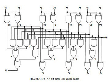
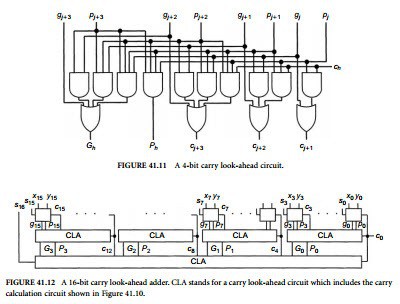
In a precedent log (What chip(s) for the ALU ?) there was the question of implementing the ADD instruction (all other ASU opcodes are derived from this). I have found some MSI and LSI chips for this, I even considered using Flash or SRAM for this purpose (128K*8 for 8+8+carry) but it doesn't fit with the spirit of the project.
I finally found satisfying explanations at http://integrated-circuit-course.blogspot.fr/2015/09/adderscarry-look-ahead-adder.html

The proposed construct is interesting, the fanout is reasonable and the bottom picture shows that a 16-bits adder is made of 4+1 Carry Lookahead logic blocks.

I don't think I will use this for this project version but I will certainly play with it in a related project that explains every gate and signal of the circuits that the Discrete YASEP uses.
 Yann Guidon / YGDES
Discussions
Become a Hackaday.io Member
Create an account to leave a comment. Already have an account? Log In.