-
First prototype
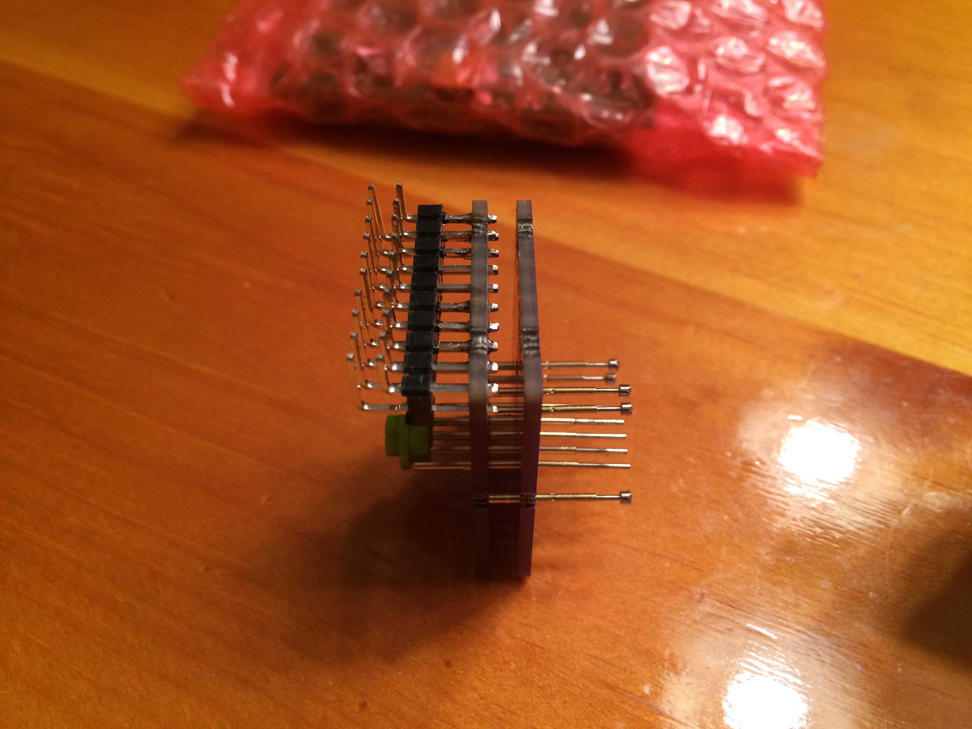
11/25/2015 at 03:12 • 0 commentsI finally got some time to work on this again. I put together the jig, soldered a blank CMIC and cap onto one of the boards, and tried to get it working with the dev kit; no dice. That's ok, I can still use the dev kit to program a chip then assemble it. First lesson learned: while the 3-pin headers look nice, there's not enough pad extending from the drill hole for the iron tip to reach. I had to use more flux than usual and just run the solder down the pogo pins until the heat spread to the pads as well. Ugly...
![]()
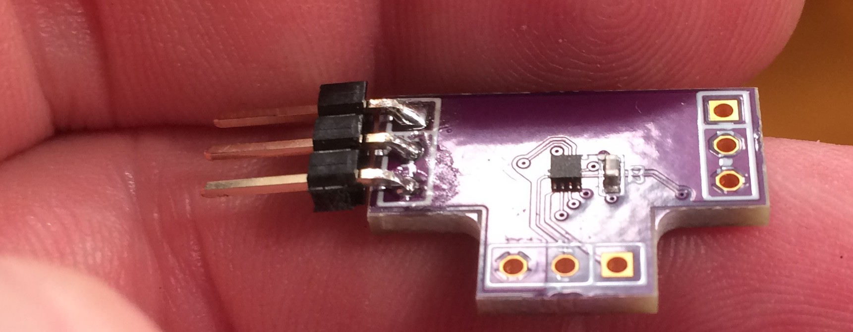
So, that was my next task. I'm glad I got the stencil, as it worked great. Since both components are on one side, it's easy enough to fry them. Second lesson learned: the capacitors are taller, and the small amount of solder paste left by using the stencil did not reliably adhere them. Other than that, the frypan worked great.
![]()
Next task: time to try it out. The DOut leg worked great. The DDelay leg flashed weirdly; With no delay, it appeared to be out of sync. Progressing lights were three-LEDs wide instead of two, illumination was too high, and coller was off. On the plus side, the overall pattern was recognizable. I suspect it's not enabling output on a 24-bit boundary, but on some other point in the data stream. Third lesson learned: don't program and populate all your prototype boards until you know if it works or not.
Time to break out my new logic analyzer.
-
Parts are in!
11/10/2015 at 14:03 • 0 commentsAll the parts are in for the original 0.5x0.7" splitter, including the caps, stencil, paste, and test/programming jig with pogo pins. Now its just a matter of pulling out the spare toaster oven and testing it out as a reflow oven.
I've never done reflow soldering yet, nor worked with anything as fine as the 0.4cm pitch CMIC, so it's all new, and a little bit scary. Ah well.. nothing like expanding your comfort zone!
-
Tiny PCB (with links)
11/03/2015 at 18:44 • 0 commentsSince I had inadvertently deleted my original circuits.io project and needed to spin a new board anyway, I shrunk it down to a 0.4x0.5" board. I had to rearrange the SJ pins some to route everything, so it's now got the following pinout:
46120 pin PCB function Programming function 1 Vcc (all three 1x3 headers) Vcc 2 DIn Vpp 3 SJ16 ID 4 n/a (tied to pin 3) 5 DDelay 6 DOut 7 Gnd (all three 1x3 headers) Gnd 8 SJ8 Mode Control 9 SJ1 SDIO 10 SJ2 SRDWB 11 n/a (tied to pin 12) 12 SJ4 SCL Note that pins 11 and 4 are tied to neighboring pins due to the proximity of their vias. That shouldn't cause any issues during programming... I hope. Once programmed, those pins are not used, so have high impedance and should be fine.
This layout, once again, ensures that the DIn connector and the five floating SJ pads can be used to program the CMIC after it's soldered to the board (but before any jumpers are closed).
These boards are tiny, and a set of three costs only $1 from OSHPark. I'm considering an entry in the square-inch contest, if nothing else to get more visibility for it. Unfortunately, I can only export gerbers from circuits.io, not .sch/.brd files, so I'd have to fire up something like KiCAD and spin yet another version for them... At least I manually edited the silkscreen layers before uploading to OSHPark so they're not so cluttered.
https://123d.circuits.io/circuits/1188853-tiny-ws2812b-delay-splitter
-
Data Flow Description
10/28/2015 at 16:13 • 0 commentsHere's a text description of how it all works, or at least should work. I've tested it on the dev kit by slowing down the oscillator, increasing the clock dividers, and upping the delay count until it resets after more than a second, then feeding a repeating 0.1s-on/0.4s-off pattern in on pin-1. I enable the LEDs on the dev board for the output pins, and pull-down jumper pins to set the delay. By slowing it down that much, I can count the pulses on D-Out and visually see how many come out before they appear on D-Delay. Now I just need to get the boards, solder parts on, and feed it a real bitstream...
To understand the text below, refresh your memory on logic truth tables and print out the logic diagram so you can follow the flow below while identifying the logic gates by name. 2-L0 is a short way of identifying 2-bit LUT0.
Oscillator/reset latch:
The oscillator can run at either 25kHz or 2MHz. Since this will be used to detect a quiet period of around 10us, a clock with a 40us pulse doesn't work, so it's configured for 2MHz (0.5us pulse). This pulse is used as the clock for DLY3 which is configured to delay only on falling edges. Assuming for the moment that nReset is high, DLY3 input follows D-In. As long DLY3 Output is high and D-In is receiving pulses, the rising edges of D-In restart the delay. When pulses stop and D-In goes low, after the delay, DLY3 output goes low. This triggers 3-L6 (acting as a RS Latch) to go low as well. However, the nReset signal this outputs is fed back into 2-L0 feeding DLY3 and ensures that DLY3 is fed a high signal. Since there's no delay on rising edges, DLY3 goes high again, and effectively generates a nResetPulse. 3-L6 stays latched low until the next D-In pulse, when nReset goes high and the reset state is lifted.
3-byte pulse generator:
D-In is fed as a clock signal to CNT1. Since CNT1 has a 3-cycle delay on reset and a 1-cycle delay on count completion, to make sure it always counts to 24 pulses, 2-L4 ensures it is restarted when either nResetPulse goes low OR every 24 pulses. After each 3-byte pulse or reset, CNT1 takes three clocks to reset and then counts to 21 before generating the next rising edge. P DLY is configured as a rising edge detector and outputs a 91ns pulse at the start of every 24th pulse.
5-bit frequency divider:
The 3-byte pulse is fed into a series of 5 D flip-flops that act as frequency dividers. The DFF's output is inverted and fed into its input. Since the three separate DFF cells don't have both Q and nQ, they're configured in nQ mode. This inverted input of nBit1, nBit2, and nBit4 is handled in the pin comparison logic below. Bits 8 and 16 are a little more complex, as they're generated by feeding the PipeDelay a de Bruijn sequence (n=2, s=2). After reset, the first two PipeDelay DFF states are (0, 0). By feeding a sequence of [1, 1, 0] as input, the outputs of internal DFFs 1 and 2 cycle through values of [(0, 0), (1, 0), (1, 1), (0, 1)], each one unique. Note that the second DFF does represent bit16 correctly, but the first DFF only matches bit8 for the first two entries in the sequence and is inverted for the second two. Therefore, Bit8 can be determined by an XNOR of both PipeDelay DFFs, which is included in the pin comparison logic below.
Pin comparisons/match detect:
After propagating through the DFFs, the five DFF states can be used to determine how many 3BytePulse signals have been seen since the last reset. There is comparison logic to compare each bit from the DFFs to its corresponding input pin. All these individual bit signals are combined with AND logic to raise a signal only when all five match. Note that, as the signal propagates through the DFFs, the individual bit values aren't necessarily correct until that propagation is complete. This may generate momentary spikes of positive output which must be accounted for below.
Enable latch:
As long as D-In is high, the 4-L0 latch will ignore the match signal from above. This gives time for the signals to propagate fully and reach a steady state. It also prevents the delayed output from including the trailing portion of the pulse that triggered the match. Once the match is detected and D-In falls, the latch is triggered and output is raised. This latch will stay triggered until nReset falls, and enables the D-Delay output through a simple AND with D-In at 2-L2. It should also be noted that, if match is high when nReset is held low, that indicates all pins are not grounded by the solder pads (value of 0), and the latch should start enabled, making a simple splitter with no delay on either leg.
-
A hiccup in how Counters work
10/25/2015 at 23:53 • 0 commentsSo I got my GreenPAK3 Dev Kit in the mail and started simulating things on it. I ran into an issue in that the counters start out on for three clock cycles before starting their counting loop. It wouldn't work to count three-byte blocks by counting off the first 24 bits, then the next 22, next 22, etc., so something else was needed. I think I've found a solution that works whereby I just reset the counter, not only at every reset interval between bitstreams, but after every three-byte block. That way I always get the 3-cycle startup pulse.
This issue also affected the reset interval counter, as it would start in its triggered state and wouldn't reset during the first three bits. For that, I ended up switching the counter to delay mode, and as long as DIn is oscillating, it stays in its last state until it stops for the reset interval and the output goes low. I added a 2bit LUT on the input so that as soon as it goes low it brings it high again for the next cycle, and reworked the latch fed by the delay cell.
I've generated a print editor snapshot which better shows the contents of each LUT and which input corresponds with which entry in the LUT. By itself, it would allow someone to recreate the circuit from a new GreenPAK Designer project.
Now for some more simulations and testing...
-
Board Layout
10/23/2015 at 19:57 • 0 commentsStupid circuits.io... I had several versions of the board and somehow deleted the current one instead of one of the older ones! I still have all the gerber files, though, and was able to order 9 of them from OSHPark.. I'll just have to trace out which pins connect to which pads. I think I have them right for the test jig, but will wait until I receive them and can verify before I order the jig boards.
I think its:
pin connection 1 Vcc 2 D-In 3 SJ 4 6 D-Out 7 Gnd 8 SJ 8 9 SJ 16 10 SJ 1 11 D-Delay 12 SJ 2 They're not very logical here, but there were a couple of priorities in deciding which pin should go where: 1) I wanted the pins used for programming the CMIC to be on D-In and the solder jumpers, 2) pin2 is Vpp (programming voltage) and input only, so I figured that should be D-In, 3) the power traces from D-In to D-Delay should be as wide as possible, and 4) with those constraints and minimal size in mind, I tried to make the board layout as simple as I could by rearranging which SJ went to which CMIC pin.
That's one of the nice things about this, and FPGAs in general. It's easy to move pins around to make the board layout simple, rather than needing to design the board to whatever pin order the chip designer went with.
WS2812B Delay Splitter
Splts a WS2812B bitstream, delaying one side by a selectable number of LEDs