 zakqwy
Panic-vias, as in "ah crap I need that pin to go way over here and it is completely surrounded by red lines".
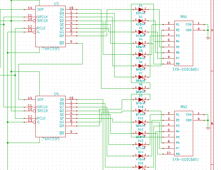
I seriously messed up the schematic (specifically around the LEDs) in order to make routing slightly easier:
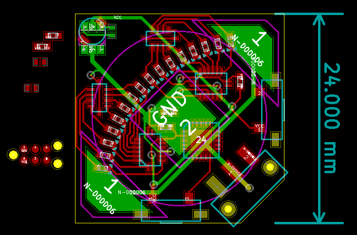
Now I get why folks don't always route between ICs and use arrows and references instead. Oh well, it gets the job done.
I started routing the PCB too; I'm trying to maintain symmetry across the 45 degree line but some of the traces don't quite line up. The sixteen (up from fourteen!) LEDs are arranged in a tedious-to-lay-out-but-satisfying ~80 degree arc centered on the on-off switch. I removed labels to improve clarity a bit, but I'm not sure it helped:
If you are a badass and use KiCad you can check the docs out in the github repo. Otherwise, stay tuned as I procrastinate on putting my Superconference talk together while attempting to get the ATtiny85 and various passive bits wired up.
Discussions
Become a Hackaday.io Member
Create an account to leave a comment. Already have an account? Log In.
Oooh, I like that arc!
Are you sure? yes | no
Thanks! KiCad doesn't have a circular pattern tool that I'm aware of (as many solid modeling programs do), but it was still pretty easy--I drew a guide arc centered on the power switch, added two LEDs at +/- 2.5 degrees off 45, then added the remainder in 5 degree increments. Getting them lined up was delightfully tedious and involved setting the snap grid to 0.05mm.
Are you sure? yes | no
Hah! Thanks for the inspiration, I just discovered there's an arbitrary-rotate feature in my normal PCB program ;)
Are you sure? yes | no
It's kinda addictive... once you can freely rotate and change to tiny grid sizes, you can pretty much do anything. I might need to do a board sometime that's deliberately chaotic and ridiculous.
Are you sure? yes | no