 zakqwy
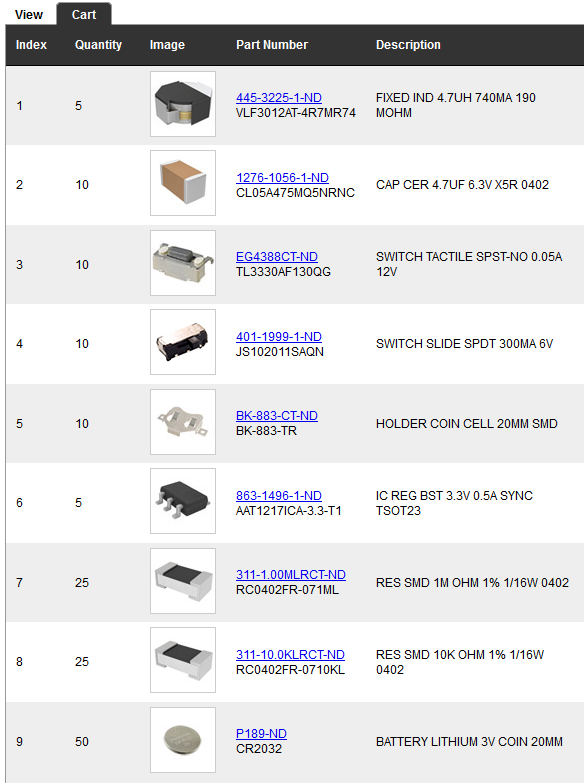
Okay, so I've never built a boost converter. Or any switching power supply, for that matter. I found this device online--hits my current requirements and it's super cheap and tiny, to boot. If you compare my schematic and the datasheet you'll see I'm pretty much ripping off their 3.3VDC reference design:

Between concerns about the high ESR of a typical coin cell, my inexperience with boost converters, and @Nick Sayer's excellent comments in response to my suggestions on #Tiny Blinky, I've decided to test this portion of the circuit before committing it to PCB (and potentially opening up another layer of complication on top of the soldering challenges I'm already facing with this project). So...
... here goes nothing, huh?
Next update will likely occur post-Superconference...
Discussions
Become a Hackaday.io Member
Create an account to leave a comment. Already have an account? Log In.
Head in hand... Oh man, sorry... I shouldn't've said anything.
I've done a boost-converter with a much larger (and slower) chip I found somewhere (like a TO-220, but with five pins), and as I recall I just grabbed the closest-but-larger-value inductor I could find on a scrapped PCB, which was quite physically-large (probably about 1/4th your entire board-size), hand-wired the whole thing (I don't think I even used a breadboard, but I don't recall), and it worked fine for my needs on a few occasions. I highly doubt you're going for UL/FCC certification... So I think you'll be fine. But I've definitely nearly ziltch switching-supply experience, and I'm just saying all this to make myself feel better about suggesting this untread-path in your project with the deadline coming up ;)
Are you sure? yes | no
General question (for @Nick Sayer, @K.C. Lee, and whoever else might be paying attention): the boost circuit I put together operates at 1.2 MHz, higher than most of the simple circuits I've put together in the past. Think I need to be careful with PCB routing and ground planes, beyond keeping the physical traces for this circuit as short as possible?
Are you sure? yes | no
If you want, I can review the layout for you. In general, you have to understand the high current path. What you want to do is to make sure that the loop area of the high currents and return path are kept to minimum. There is usually a section in the datasheet for the layout notes.
The AP3012 chip I used is 1.5MHz
layout here: https://hackaday.io/project/2145-smps-replacement-for-7805/log/21303-sepic-converter
The AAC2120 buck converter in another project is 1.8MHz. Unfortunately the layout might be a bit on the complex side. :)
https://github.com/FPGA-Computer/Swiftlet/tree/master/Ver%200.0%20Rel%200/Eagle%20PCB
Are you sure? yes | no
Great info--thanks! I'll look through your layouts, test the parts when they arrive, and probably update my layout a bit as needed--at which point I may take you up on that review :-)
Are you sure? yes | no
Keep the traces short, and keep the high-current path very low impedance (wide traces if not sub-planes). That said, if you're designing for < 100 mA, the bar is a bit lower. But the goal is not only cleaner output power, it's less radiated switching noise.
Another thing to watch out for is to insure that everything in the entire design operates at lower than 1.705 MHz, if possible. If you do that, and if the device is battery powered, then you (generally speaking) are exempt from most of the testing and labeling requirements nonsense that goes along with FCC Part 15 (see 15.103).
Are you sure? yes | no
FYI: current loops. Always consider the return path including ground. The idea is to keep the area enclosed by the overall path small and to use thick tracks. Avoid using vias along the path if you can.
Path 1: Cin+ to Vin pin to inductor to SW pin to AAT1217; Return: Gnd back to Cin -
Path 2: L1 to SW to Vout to Cout+; Return: Cout- to ground to Cin-
Are you sure? yes | no
http://www.skyworksinc.com/Product/1240/AAT1217
There are eval board and gerber file in the download section.
Are you sure? yes | no
Nice. I'm going to build my own for now (I've recently restocked my supply of blank FR4).
Are you sure? yes | no
That's kind of a beefy inductor... What about 587-2044-1-ND?
Are you sure? yes | no
Hmm, good thought. I'll see if I can update the order. Thanks!
Are you sure? yes | no
I got burnt using that series of inductors. Seems like they saturates a lot sooner than. Even the cheap Chinese inductors I replaced it works a lot better.
https://hackaday.io/project/4993-dual-channel-battery-chargeranalyzer/log/21302-we-need-bigger-inductors
Are you sure? yes | no
Hmm.. good to know. Maybe I'll see if I can try both options. The ones I originally spec'd seem like they should work, but their 740mA current capacity is a bit huge for my project.
Are you sure? yes | no