Edit: See also More 2369, with more caps !
With a sporadic and limited access to the workshop (at last !) I can finally try new ideas ! I have meanwhile received 9K PMBT2369 in SMD but I decided to use the old stock of 50pc 2N2369A in metal can, that was waiting in a small bag that I received from various sources... What can be closer to the CDC era ? (A motor-generator ? :-P)
This is a "mixed bag" with at least 2 sources or makers, some with golden legs, and I decided to test them. Just because I now have a better tester and it's good to see if/how the different types differ...
Most "golden" parts fall in the lower bins and the tinned ones have overall the best gain. I made 3 bins :
- < 60 (lowest is 46)
- < 84
- higher (a few up to 114 and one at 119)
and then I use the lower gain ones to build the RingO, with 9 parts to give a low-enough frequency that makes 'scoping reasonable.
I could have made a > 100 bin but
- I just wanted to have a look at the spec spread
- I wanted to weed out the lemons (and use them first to establish a baseline)
- the temperature sensitivity makes it moot.
After Tim's experiments, I chose from my parts bins :
- Rc = 470 (so I can test from 2V to 5Vcc) in 0805
- Rb = 220 (that's what I have in stock right now, close enough)
Afterthought : I should have tried 100 Ohms for Rb. Or even 47/50 ohms maybe....
After-afterthought : or 330 ohms (see near the end)
And the soldering iron was turned on !
- For the sake of simplicity I omitted the caps. They used too much room. Next time I'll look at the SMD stock.
- I added 1nF to decouple every pair of transistor (that's 5nF but spread to ease HF transients)
- I found some partial reels of SMD Schottky diodes but once again, decided to not use them yet.
So I wanted to establish a baseline for speed and more importantly : explore the power vs speed envelope because... Tim found that a LOT of power was wasted. I would like to get a gate that is still "pretty fast" and yet consumes at least 10 times less power.
For the measurements I used a 200MHz digital scope with 10x probe. The output waveform is pretty nice and quite square-y :-) No funky feature is noticed, it's plain old RTL and I didn't bother to measure the rise/fall time because the measurement circuit is not optimised.
Still it's very telling.
2V:
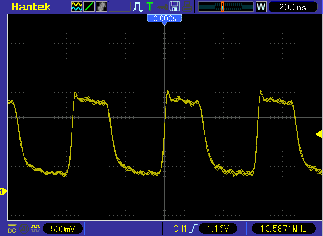
2.5V:
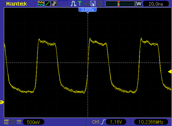
3V:
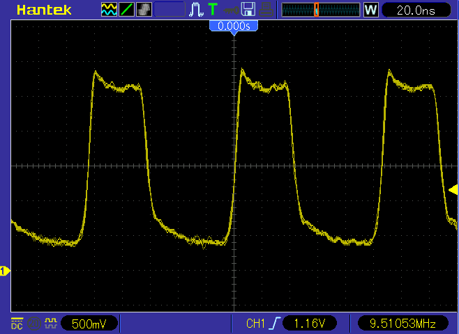
3.5V:
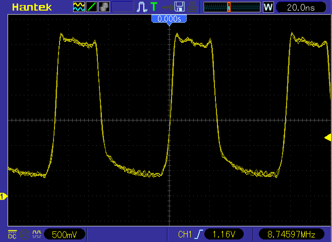
4V:
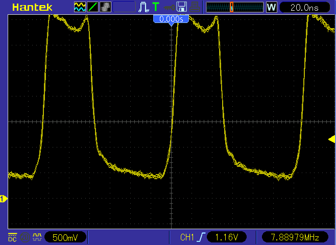
4.5V:
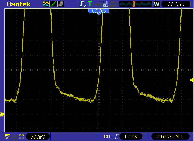
5V:
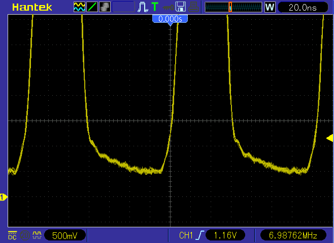
Rise time is about 5ns. Which is odd since I expected that RC would dominate it.
In fact something else is happening : it seems that the transistor has a harder work to totally saturate and keep Vce sat to a sufficiently low value. This in turn reduces the frequency because the transistor turns off later.
At 5V the circuit doesn't seem to get hot, maybe thanks to the help of the metal cans and the resistors directly soldered to thick metal that can spread the heat.
You can find a curve that is similar to what Tim found already :
Vcc  Total   Freq.
5V   123mA   6.98MHz  <= never mind.
4.5V 109     7.37
4V    97     7.77
3.5V  81     8.61
3V    69     9.42 <= why waste so much power ?
2.5V  55    10.16
2.25  47    10.48
2V    40    10.55 <= sweet spot !
1.75  33    10.48
1.5V  26    10.06
1.25  18     9.13
1V    11     7.34  <= wow, that's still good :-D
The frequency is measured by the scope but not finely calibrated. My HP freqmeter wouldn't accept the raw signal, something to do with ringing and probe impedance, I'll check that later. Still you can find the important features.
With my choice of parts, I find that the sweet spot is in the 1.75V-2.25V range, as roughly expected, so I'm pretty happy ! But there is more to that curve.
Let's now compute and deduce some numbers :
Vcc  mA Total Freq. mW Total mW/MHz
5     123     6.89    615      89
4.5   109     7.37    490      66.5
4      97     7.77    388      50     5V/4V=> *1.8
3.5    81     8.61    283      32
3      69     9.42    207      22     4V/3V=> *2.3
2.5    55    10.16    137      13.5
2.25   47    10.48    106      10.1
2      40    10.55     80       7.6   3V/2V=> *2.9
1.75   33    10.48     57       5.43
1.5    26    10.06     39       3.88
1.25   18     9.13     23       2.52
1      11     7.34     11       1.5   2V/1V=> *5
The power/speed ratio decreases faster than the voltage ! (due to the Vbe effect and the RI² factor)
Going from 3Vcc to 2Vcc gives you almost 3x power advantage for 10% speed gain... And over the "sweet spot" frequency range (1.75-2.25V), the power (almost) doubles !
At 2Vcc, each transistor draws less than 1mW and is at its fastest point, using a very simple circuit. If you consider a 3-input gate with all the inputs on, the current is shared among the 3 transistors so it can go lower but then, the power from all the base currents becomes prevalent.
Aparte:
If you consider the reliability considerations of the CDC6600, drawing less power would have been very easy and the inherent costs (power supply, cooling etc.) are insane. See the Living Computer Museum video where they explain that the chilling water tower and the piping cost them much more than the rest ! And heat management was a defining trait of these machines. So it's good to have the numbers to vindicate my quest to reduce the supply voltage.
So what convinced Seymour Cray to burn so much power and explode the budgets ?
Edit: It seems the answer is in fig.17 of p.26 of the "Thornton book" : "buy" as much current as they can so the rise time of the transistor would be negligible compared to the RC load of the node. Furthermore the power supply is not capacitor-filtered but direct from tri-400Hz which has a 2400Hz ripple so they needed that margin too... I suppose they studied the capacitor method but the load's RC might have been a dominant speed limiter. This is a cautionary tale for the results of RingO circuits : they don't directly apply to real circuits.
Something else is interesting, I had to share it ;-)
This circuit tests the basic inverter but you can't make a computer with this. The minimal theoretical fanout is 2, 3 becomes almost practical, VLSI CMOS chips target 4, and you need at least 5 or more to make anything interesting. Yet a majority of the practical cases are 2 or 3... But the higher, the better !!!
The CDC6600 has some interesting "rules of thumb" concerning fanout:
- FO=5 for intra-module circuits
- FO=2 for inter-module transmission
- Not more than 6 collectors tied together
(see p.25 of the Thornton book) and I'd like to check if they still apply here.
The first thing is to reduce the pull-up resistor as the number of gates increases. Page 25 tells that CDC adjusts it, as well as Rb. Let's compare the values of Rc (called RL) with the E12 series :-)
    target  E12
FO1 : 470   470
FO2 : 235   220  (240 in E24)
FO3 : 156   150
FO4 : 117   120
FO5 :  94   100
FO6 :  78    82
FO7 :  67    68
FO8 :  58    56
Nice fit, no ? :-)
But for a good fanout, the precision (or exact match) of the pull-up is not critical. Two things are, though :
- Drive the base hard enough to lower the output well enough. CDC specifies < 0.2V, which occurs at Ib=1mA (see: the Thornton book, p.22) => the gain is low at the highest frequencies so the base current increases during transients, up to 3mA (see below)
- Pump enough current through the collector while remaining within the limits of power dissipation : while conducting, ideally, the transistor dissipates (Ib*Vbe)+(Ic*Vce)=0.7+2mW=2.7mW in the best, continuous case (supposing 10mA in the collector). In practice, the transients add more current here and there.... but this is compensated by the "off" states. Here we already see that in average, a transistor shouldn't dissipate more than 1.5mW in average. RL burns the majority of the total power, all the time !
The gain would directly dictate the fanout : at Ib=1mA and Ic=10mA we would expect a fanout of 10 but it's not working like that. First, the base current would increase even higher (during transients) and the base current is not directly driven by the driving transistor, which actually short-circuits it. The collector swings from 0 to 1.2V, or 0% to 20% of 6Vcc, Ib would receive about 80% of Ic. The fanout would be in the range of 3 to 4 (not counting PCB parasitics)
By the way, the "Thornton book" ("Design of a computer : the Control Data 6600") makes more sense now, and I can better read between the lines of several paragraphs that were cryptic. I had forgotten that the "diode equivalent" of Vbe should limit the value of the input voltage and the Rb must be lower than the 220 I chose before.
If Vin=1.2V, with Vbe=0.7V, then Urb = 1.2-0.7= 0.5V : the base resistor drops half a Volt, which is not the case in my prototype (and probably not @Tim's ?) but it's easy to estimate the value : Ib=1mA, Urb=0.5 so Rb=Urb/Ib=500 ohms (wait, what ? that's not consistent with my estimates by a factor of 10 ! And the CDC6600 has Rb about 150 ohms so why is it different ? Poor transient gain ?)
TODO : measure the base resistor drop. I 'scoped the traces above at the collector node but I didn't trace the base voltage (though it's expected to wiggle around 0.7V) and it seems the base resistor voltage is much higher, since the collector can rise up to Vcc (must be re-checked !) despite the lower value : 220 < 500 as calculated in the previous paragraph. Something is not right and I'll have to retry with 47 ohms. Or even a trimpot.
Base-collector "Baker clamps" are cool but as Tim noted, they reduce the margin.
However, 2 silicon diodes in series (between the ground/emitter and the collector) would drop about 1.4V, which is about right for the CDC logic levels. That would be only 2 diodes per gate output with a higher tolerance than the Schottky clamp diodes, it would preserve the noise margin and the base current would be easily controlled by the base resistor.
The problem would be speed again because silicon diodes exhibit a non-negligible capacitance... PMBT2369 is rated at 4pF max while the planar 1N4148 is also rated at 4pF and 4ns (whatever this actually means and whether it applies).
EDIT: BA243 is 1.5pF and capacitors in series have lower equivalent capacitance. Furthermore the diode would not switch from reverse to forward bias, which avoids a trouble-making behaviour (unless your name is @Ted Yapo and you want to build a Diode Clock) but it would work as a sort of Zener and go from 0V to 1.2V
Another consideration : The PMBT2369 datasheet shows hFE minimum of 20. Gain should be considered "low" during transients and many measurements are under the condition "Ic = 10 mA; Ic = 1 mA" (actual gain=10) and the base current reaches 3mA for the rise time measurement (and -1.5mA for falling time). The tripled current would explain why practical circuits have such a low base resistor...
More considerations in the comments section :-)
... and more apologies for editing this log so many times ;-)
PS: Great find, Tim, you didn't say it loud enough though ;-)
 Yann Guidon / YGDES
Discussions
Become a Hackaday.io Member
Create an account to leave a comment. Already have an account? Log In.
>PS: Great find, Tim, you didn't say it loud enough though ;-)
Yeah, sneaked it in as an incremental update ;-)
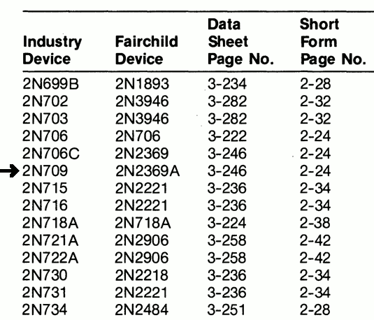
But OTOH, these things are usually decided by marketing people. So maybe they found that their current customer base could suffer through the pain of replacing the 2N709 with the 2N2369A. That doesn't mean that it is equivalent in each and every metric. Also the "A" is suspicious. Special binning?
Are you sure? yes | no
I have NO way to know.....
maybe a new line or process that was tuned to emulate the old 709 but cheaper...
Look at the follow-up of this log :-D The capacitors do wonders...
Are you sure? yes | no
My fanout estimates don't make sense, when I add the constraint of a common logic level of 1.2V.
And the case of FO=1 degenerates nicely to the case where Rb can disappear. So we have Rc = (Vcc-Vbe)/1mA = 1.3K... but this would not work as nicely because the swing would be low and the higher resistance of RC would oppose the pull-up current that moves the charges. A coupling capacitor would be more effective then, with Rc = 470 as before, RB=1K with 47pF (or something) in parallel. The higher swing of the driving collector signal would be pretty beneficial...
In the case of Vcc=2V (in my "sweet spot") and a 1.2V signal level, we would then ideally have Rb = Rc (for the single inverter case). This is because since Vbe=0.7V = U high/2 = Vcc/3 (approx.) then Vbe = Vrc = Vrb.
In my prototype, Rc = 470 and Rb = 220, with a total of 690 ohm. To make Rc=Rb, that would make them 690/2= 330 (closest E12 series). The parallel capacitor would be mandatory to maintain performance. Vcc decoupling to GND is also critical to prevent all sorts of parasitic effects...
Are you sure? yes | no
According to Optimizing Resistors in the PMBT2369 Ring Oscillator Rb=150 and RC=680 on the CDC6600. This contradicts the calculations (they give 500) but it's still close to 220 that I used.
680 is close to the total 470+220=690 that I used. So the pure U=R×I law doesn't hold in these cases...
Furthermore I'm almost sure that I probed the collector voltage that reached about Vcc, and not a reduced version (the scope screenshots prove it). So something strange happens somewhere...
Are you sure? yes | no
They chose 680 for a FO=1 and supposedly divided it for higher fanout. There was a comment somewhere about 680 Ohm being the highest resistor. Maybe there was also more finetuning, so they used different resistors even for FO=1.
Regarding your supply voltage comment: Generally, don't be confused by RC time constant. A capacitor is charged by a current C*V=I*t! Therefore, only the current going into the devices is relevant not the resistors that were chosen to generate it. So the currently supply should always be a good indicator of switching speed, if it is dominated by capacitance charging.
I believe the choice of 6V supply is purely due to droop. If you consider that deltaI=deltaVCC/R, then it's obvious that going for a higher supply voltage, and hence higher R, will lead to a more stable supply with less current variation.
One can obviously go for a lower supply, but then both collector and base resistor need to be adjusted.
Are you sure? yes | no
Yes, that would make some sense...
We are spoiled in 2020 with abundant sources of cheap DC/DC converter modules :-D
But now that I think of it : I now have a lifetime stock of power Ge transistors. Their low Vbe would make them great candidates for low voltage discrete linear regulators :-D
Are you sure? yes | no
Yes, Thornton mentions 680 ohms at the bottom of page 25 of his book. I didn't find Rb yet though.
Are you sure? yes | no
I got Rb=150 Ohm from the schemtic of the twisted pair transmitter.
On the other hand, one can deduce from the table that Ib=1mA and 1.2 V - 0.8 V = 0.4 V drops accross Rb. That would mean Rb=400 Ohm, which seems a bit too much.
Are you sure? yes | no
R1 on figure 20 ?
Are you sure? yes | no
@Tim can you check my latest updates ?
I can't access my workshop before "some time" so I need you to verify the voltage drop across the Rb.
My estimates don't match with my measurements...
What about Rb=50 ohms ?
Are you sure? yes | no
I might have found the answer in the datasheet : the transient base current can be quite high, 3mA instead of 1mA... That means a pretty low gain.
Are you sure? yes | no
Man, that's a cliffhanger :)
Are you sure? yes | no
wait, there's more, additional bonus coming soon, stay tuned :-D
Are you sure? yes | no
Ah... you sneaked an update in. Now I look like a lunatic in my initial post :)
Well, nice results. Your RINGO is of lengths 9? So you get a tpd of 5.3 ns at the optimum and ~5mA bias. Looks very similar to what I got.
Are you sure? yes | no
Yes I'm almost at 5ns with minimal effort. Using the worst gains, no cap and no clamp. It can only go faster from there ;-)
Using 9 inverters makes it easier to probe and it is more typical of a normal circuit. The waveform has more time/room to settle and can display some DC-related effects.
Are you sure? yes | no
It's weird that the falling edge looks slower than the rising edge? Usually it's the other way round.
Are you sure? yes | no
yes, the transistor manages to go low, but not "hard low". I would suggest that this is because Ib is not high enough (and reduce Rb to 100 or even 50) but this is contradicted by the case of 5V where the current increases but the voltage is barely close to the limit of 0.6V...
The capacitor would help a lot.
Are you sure? yes | no