TLDR: I’ve hit my first self imposed deadline and I’m running a bit behind schedule. There were some PCB design issues that I noticed and then fixed. Also, the bulk of the analog HDL is done, but not ready for synthesis. Once those issues are resolved I’ll do a more detailed post on how I’ve structured the 3 subsections of the analog module. In the meantime, I have uploaded a snapshot of where I’m at with the PCB and Verilog.

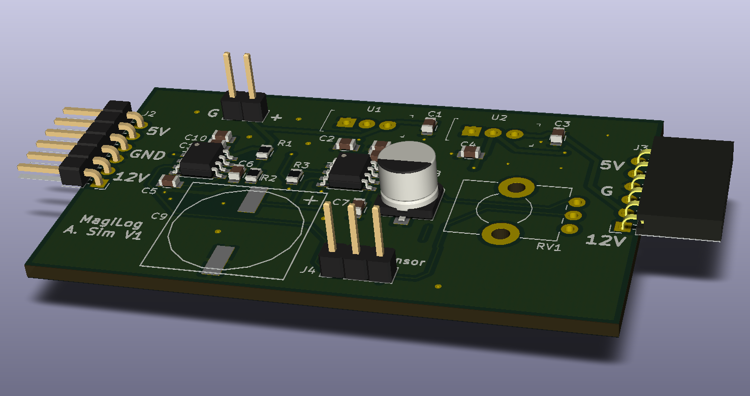
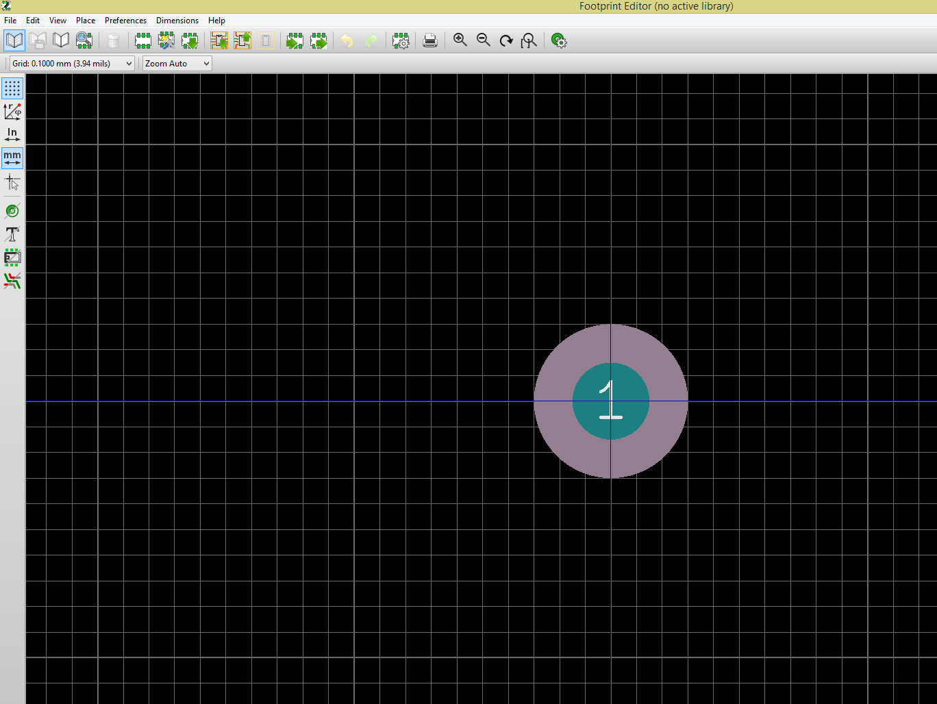
Over the last week I noticed a few issues with my board layout. Some of the silkscreens were poorly placed, a bunch of vias were just floating in the abyss and I had mis-sized a capacitor. The silkscreen issues were easy to fix, just move and/or resize some text. The other two issues were a bit more involved. First fix was growing the board to accommodate the larger but properly sized capacitor footprint. As it turns out when I updated my track/via parameters to what OSHPark recommends it changed how any new vias would be formed. Instead of properly stitching where I wanted to stitch the ground plane it would create a via that was completely isolated from any other copper. After some googling I was able to get around this by creating a custom through-hole part that would become the base part for any vias I wanted to stitch with.

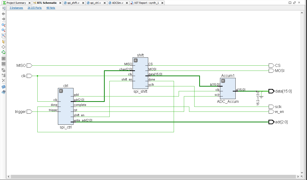
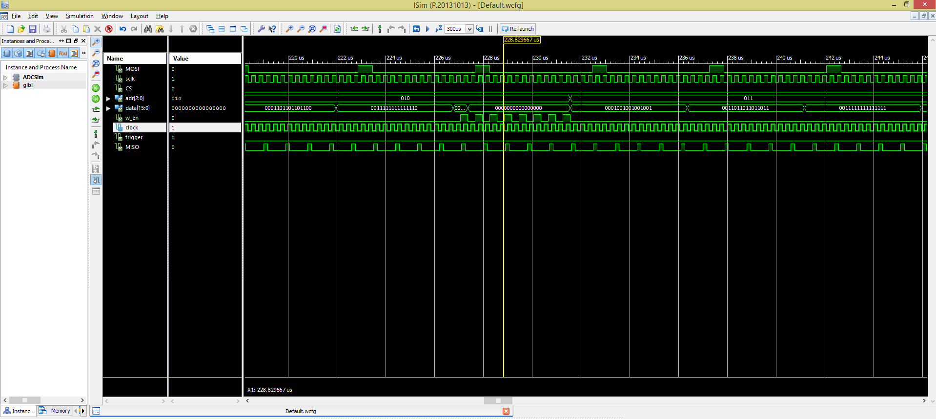
On the Verilog side of things, I had a design that ran well in simulation but when I tried to synthesize it I ran into unwanted optimizations or errors. Essentially the issue I’m running into is that not all code that works in simulation can be synthesized even if you don’t use any non-synthesizable parts of the Verilog language. I have never been very good at Verilog, so coming back to it after many years debugging is kinda difficult. The error messages you get with HDL designs are not as useful as their software equivalents, so it feels like I’m running blind to a degree.

Overall my FSM design is far from good and it’s causing new issues as I try to fix old ones. I was able to get rid of one issue where a reg was optimized away but in doing so I now get unwanted (but not function breaking) behavior in the reset portion of the code. I end up resetting the accumulator that adds up the ADC readings a bunch of times instead of just once. It doesn’t impact the function of things but it’s something that needs to be fixed.

The bigger issue is that this new snapshot of code won’t complete synthesis without throwing an error. After one more round of attempted fixes I’ll probably take a step back and focus on the digital sim PCB and HDL module that I wanted to get done this week. Hopefully after coming back to it with fresh eyes I’ll be able to get things working on chip.
 Nigel
Nigel
Discussions
Become a Hackaday.io Member
Create an account to leave a comment. Already have an account? Log In.