-
Tiny progress
01/11/2016 at 03:48 • 0 commentsI received SMD resistor networks that pack 4× 0603 × 1K into a 1206 form factor, this will help save a little room here and there. This is the kind of part that, when you start to use it, you wonder why you didn't before...
Delivery of the AT49BV162A : at last! They were worth the wait, I can proceed with the rest...
I should add pull-down resistors on the input data signals...
I'm already thinking about how I'll integrate the design in the #Discrete YASEP. The availability of a 1M×8 chip allows me to just drive the 5th segment with its own decoder, in the P1B Display page. New modes become possible since all the segments will be completely decoded! An octal mode might even be possible...
-
Stack-based programming
12/18/2015 at 06:24 • 0 commentsNo I won't talk about FORTH ;-)
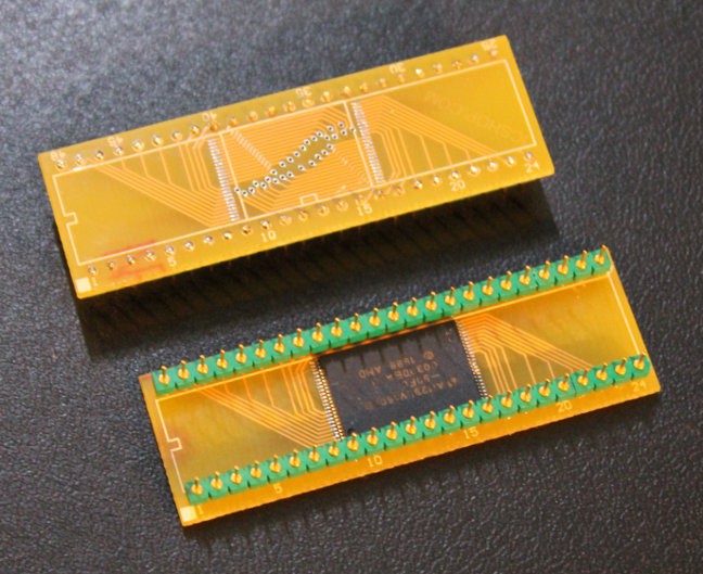
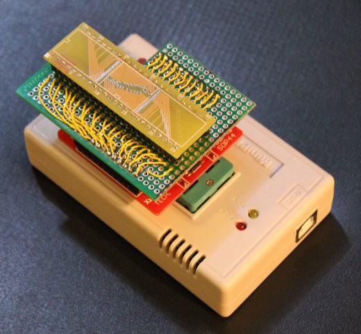
Today I received a pair of little adapter boards for TSOP-48. The cheaper chinese adapters are "wide" and I prefer the narrow ones that match the DIP48 format because it's more compact. I'll use this assembly to prototype the whole DYPLED board, on a prototype-style drilled board so I need something to flash the chip a few times while I code and verify the contents of the Flash array.
![]()
As soon as I got the boards, I soldered one AM29LV160DB. The pins are soldered in the opposite side because this particular chip has a reversed pinout (see other episodes such as Flash EEPROM adventures (and a happy end)...). I have another board for the other chip reference that should arrive soon, with a standard pinout and 5V tolerance :-)
Why did I choose this title for the log ? Because when I need to program the module, it makes a weird stack of adapters :-D
![]()
-
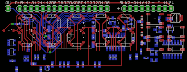
Preliminary layout
12/16/2015 at 20:59 • 0 commentsIt appears that the module will be SIP and not DIP.
![]()
Update:
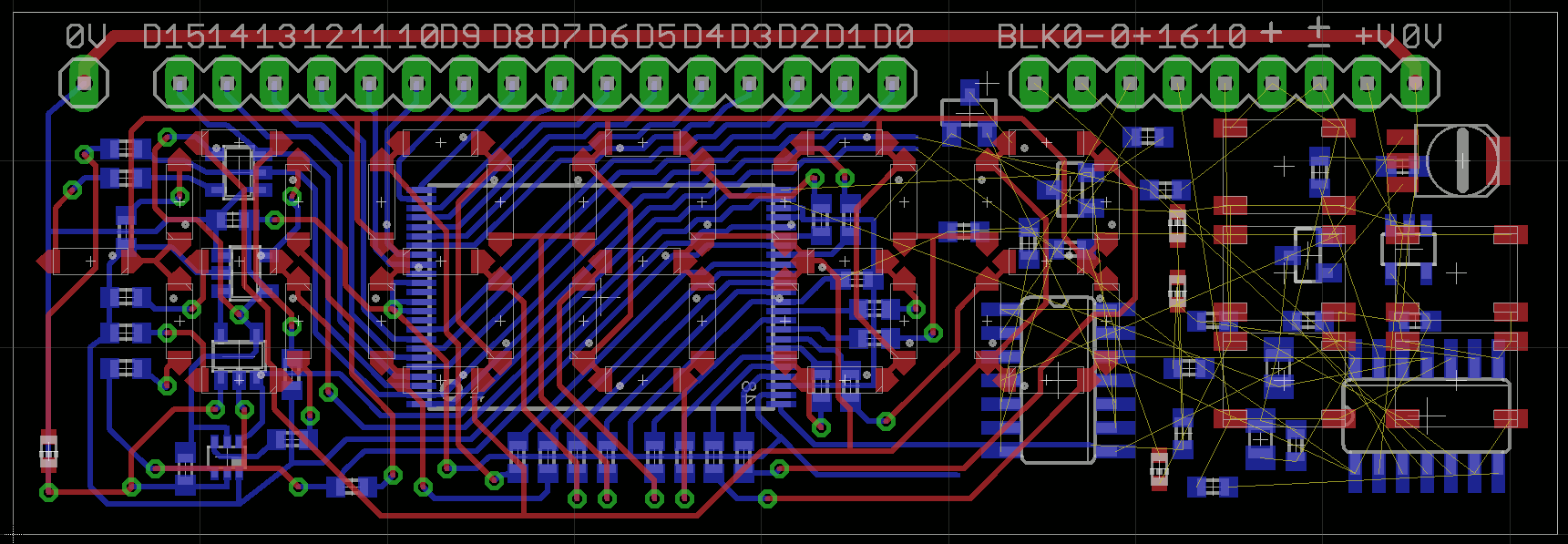
so far the board's dimension is 83×27mm and I'm amazed that routing was so smooth :-D It's not finished but I can already see how it will be.
![]()
The tracks are very dense and I'm surprised that everything "just fits". The part on the left looked almost impossible to route initially. The part on the right will be less difficult, I think :-)
-
Some updates
12/15/2015 at 20:04 • 0 commentsHere are the latest news :-)
I will use warm white LEDs for the segments, so they are easier for the eyes.
I fixed the blanking system to avoid power drain when grounded.
I found the reel of double Schottky diodes (it was hiding with the transistors, hey it's SOT23 too...)
I've refined the mode displays : 0603 LEDs with very dim light and different colors (the current mode is easier to visualise, color is faster to "grasp" than precise position)
I'm entering the schematics in EAGLE and checking all the parts, their pinout, their footprints, prices, availability and values...
What's left ?
- get/make the footprint for the flat SMD pushbuttons
- check the phases and the decimal decoder
- layout
- mix/swap all the inputs and outputs for easier routing
- create a program that generates the flash's contents according to the routing matrix
and so on...
-
Adjustable PWM oscillator
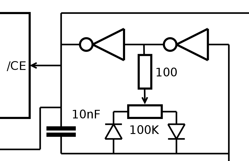
12/09/2015 at 05:52 • 0 commentsThe most delicate piece of electronics in this project is the variable duty-cycle oscillator. It has two functions : drive the divide-by-two flip-flop to alternate between odd and even addresses (output LED multiplexing) and also dim the LEDs (through the /OE pin of the Flash chip).
The frequency should not change much because the output multiplexing should be smooth, well above 1KHz. Only the duty cycle (percentage "on") should change so this precludes a lot of variable frequency oscillators.
So I started from the #Charleplex Xmas Tree without uC oscillator topology and remembered a little "trick" I saw while looking at other oscillators recently. I have already played with asymetric oscillators so I was familiar with using two diodes to select one resistor for one phase, and another resistor for the other phase. What I saw is to instead use a trimmer where the brush is the common output and the diodes are on both ends. This keeps the average resistance almost constant, the frequency does not change much but the high vs low time are proportional to the brush position.
There is another problem as well. The eyes have a logarithmic response but SMT adjustable resistors are linear only. This reduces the "interesting" range to a small angle of rotation. My solution is a very high ratio between the trimmer's value and the series resistance that controls the minimum on and off time.
![]()
In my experiments, I found a reel of 100K Ohms trimmers. I started with a 1K series resistor but that was still too high. 100 Ohms provide a 1/1000 ratio and the luminosity is still good when using a LED without series resistance (and I'm not counting the 1/2 duty of multiplexing).
The diodes are Schottky in SMB package. I don't have anything else, it's not the thinnest but the trimmer is the less thin device in the module (1.3mm thick) so it's not so important.
For the frequency, 100nF oscillates too slowly, I see flickering. But 10nF is good. Varying the duty cycle changes the frequency by 20% at most, I suppose that the diodes add non-linearities. I measure about 1200Hz. It's not yet divided by 2 and I think 600Hz is too slow so I'll try to find 2nF caps.
At 1.8nF, the frequency is around 6KHz, or 3KHz after the mux divider. No flicker is perceptible.
![]()
I soldered the SMT parts (diodes and trimmer) on a small proto PCB. The trimmer is not easy to adjust but it's not something that would be operated often...
20170429:
@Frank Buss found a study about pulsed LEDs (see PWM test) that shows that flicker can be perceptible up to 3KHz so my experiments seem to be vindicated :-)
-
A dumb bistable
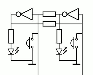
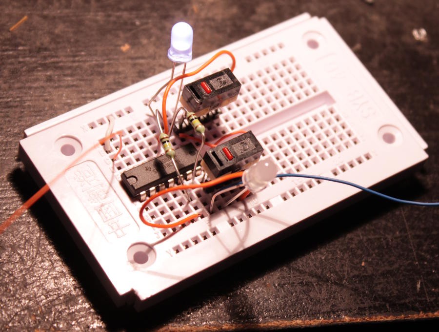
12/09/2015 at 02:48 • 0 commentsI know I could have done this with a pair of transistors but... The HC04 is more handy.
![]()
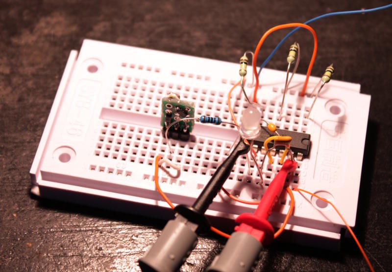
Just to be sure, I implemented the circuit and it worked (as soon as it was correctly wired, as usual :-P)
I love how simple it is. It's easy to look down at simple, dumb inverters but a few resistors and they become very versatile :-)
![]() And to be honest, it got on tracks thanks to #Charleplex Xmas Tree without uC (@K.C. Lee will even recognize the oscillator topology of the other part of the circuit)
And to be honest, it got on tracks thanks to #Charleplex Xmas Tree without uC (@K.C. Lee will even recognize the oscillator topology of the other part of the circuit) -
Little enhancements
12/08/2015 at 22:52 • 0 commentsI have solved the AND issue :-)
The sign bit gets ANDed with the signed/unsigned mode bit. However a AND gate is pretty annoying to do "on the cheap". It's a "slow" operation so a dumb transistor might work but the diverse voltage/current considerations make it unpractical.
I could boost the signal with one inverter gate but they are all used. One Flip-Flop function could be borrowed from the remaining half of the 74HC74 but it has a kind of "forbidden state" (both /CLR and /SET active) that I want to avoid (it's nicely solved with the HC04).
OTOH there is this other FF that sits unused. The "trick" is to let it "copy" the sign bit (using the free-running clock) and "block" the output with the /CLR input from the mode flip-flop. It's ugly but no additional part is required and all the ICs are used to their fullest !
Well, one input is not yet used : address bit n°19 of the Flash array. I could add another mode but... what ? (octal won't fit by a little, btw)
Update: the remaining mode will be "show leading 0s" but this will only be available by tying a pin to GND, no fancy push-button there... It defaults to "hide" to save some power.
-
Cost optimisation
12/07/2015 at 19:53 • 0 commentsOne design rule of this project (and #Discrete YASEP) is to keep the part cost as low as possible. This in turn influences the choice and function of the parts. For example, this explains why I chose a Flash chip instead of a microcontroller, a CPLD or a dedicated decoder. In turn, this opens new kinds of functionalities.
Note : all the following prices are for bulk purchase on eBay or aliexpress, prices will vary and I chose an opportunistic approach where the parts I find influence the design, and not the contrary. It's different from a "perennial" design where parts are bought from Mouser/Digikey/Farnell/Element14 where obsolete parts are not stocked but you can buy as many pieces as you need and not much more. Overstocking lots from brokers counters the cost savings of not buying more than you need. However I have no idea how many modules I'll build (maybe 50-100 for the #Discrete YASEP) so it's a rough estimation. PCB costs and soldering are not counted either...
- AT49VB162AT : Found a lot with a unit price of 0.5$/pc
- 4014 LED : 0.01$/pc, ×36 = > 0.36$
- 74HC04 : 0.064$/pc
- 74HC74 : 0.125$/pc
- LDO 3.2V : old stock, price forgotten, let's say 0.1$/pc
- Mode LEDs : not chosen yet but the 4 would cost < 0.1$
- 2× N-MOSFET : I got a reel of 2N7002, forgot the price, let's say 0.05$
- 2× P-MOSFET : TBD
- Trimmer: TBD (0.2$ ?)
- buttons: 0.04×4=0.16$
- 2×16 pins : 0.32$ ?
- 26 resistors : values TBD, old stock, less than 0.05$
- Capacitors : I have reels of 100nF in several footprints, virtually free
So if thousands of these modules were manufactured, the parts cost would be around 2$. I can probably even reduce it a tiny bit more by dropping the 2N7002, the 74HC74 could drive the low-side directly, since the current is within the working range... But PCB fabrication, soldering, prototyping, yield and many other factors increase the overall price !
-
Decoding the extra digit
12/07/2015 at 08:02 • 1 commentThe decimal display is a nice additional feature but it puts some more pressure on the design. The pressure was reduced when I found that the 74HC74 could drive the MOSFET directly (instead of using the Flash to decode one bit to 2 outputs) but the requirement remains: the display needs a fifth digit that can range from 1 to 6.
With 3 bits, it's not too hard to decode 3 bits to the required 6 segments, using a few diodes.
digit A B C D E F G 1 * * X 2 * * * * X * 3 * * * * X * - Segment F is not implemented.
- Segments A, D and G are on for 2 OR 3
- Segment E is on for 2 (directly)
- Segment C is on for 1 OR 3
- Segment B is on for 1 OR 2 OR 3Total : 7 diodes only. However this limits the display range to 39999(d). Adding the 3 other digits (4, 5 and 6) is a bit more tricky but the principle is roughly the same, adding the F segment but trying to squeeze as many codes inside 4 bits. 3 bits are enough to code values from 0 to 7 but hopefully we can predecode some things and avoid using an external 74HC138...
digit A B C D E F G 1 * * 2 * * * * * 3 * * * * * 4 * * * * 5 * * * * * 6 * * * * * * At this point, the codes 1 to 6 should be recoded to an intermediate 4-bits code which requires only OR logic (implemented with diodes).
The segments A-D-G are often ON at the same time so it's a first line of optimisation. Negative logic is another angle of attack (it worked well with the diode matrix). 5 and 6 differ only by the F segment so there is more hope to find an intermediary recoding.
One code (Z) is assigned to segments A-D-G, which covers codes 2-3-5-6.
Code Y controls segments B and C for the codes 1-3-4.
Sor far we have:
- 1 = Y
- 3 = Z + Y4 codes remain with only 2 bits left. Bit X is assigned to segments C-F-G to form one part of the numbers 4-5-6. X overlaps with Y (segment C) and Z (G) but they are ORed with the diodes so there is no problem.
- 4 = X + Y
- 5 = X + ZDigits 2 and 6 remain and get code W, which directly controls the E segment.
- 6 = W + X + Z
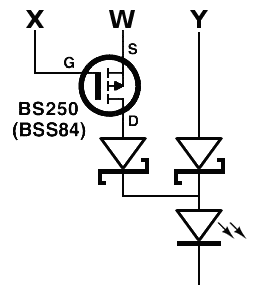
This pre-decoding requires a few diodes to transform the 4-bits WXYZ code (output by the Flash chip's 4 data lines) into a 7-segments digit. However a tiny extra logic is required to implement the digit 2. This is not convenient because it can't be solved with a diode, as a OR function. A AND function is required, hopefully implemented with a single transistor.
2 and 6 differ by the X code:
- 2 = W + Z (X=0)
- 6 = W + X + Z (X=1)So the B segment's equation would be
B = Y or ( W and /X )
W is active ONLY for 6 and 2 so the electronics can be simplified, using a P-MOSFET (and a diode). I'll have to check this though...
![]()
The resulting equations are:
0 =
1 =         Y
2 = W +         Z
3 =         Y + Z
4 =     X + Y
5 =     X +     Z
6 = W + X +     Z
Converted in Hexadecimal with W=1, X=2, Y=4, Z=8,
0 = 0
1 = 4
2 = 9
3 = C
4 = 6
5 = A
6 = B
(All the codes are different so we're good).
The 4 pre-codes are :
![]()
Outside the Flash, we have :
A = Z
B = Y or (W and /X)
C = X or Y
D = Z
E = W
F = X
G = X or Z
4 segments are directly driven by the Flash output. The others are 3× OR2. That's 6 diodes and one P-FET only :-)
Update 20151214
While laying out the PCB I realise that some diodes could be saved thanks to the multiplexing... Is it possible to use only 2 output pins ? This would simplify the rest of the PCB layout and segment assignment.
ph.1 ph.2 A = D = Z * B = Y or (W and /X) * * C = X or Y * * E = W * F = X * G = X or Z * * Some things are pretty easy :
- E and F's cathodes are connected to the phase 1 low-side transistor.
- A and D's cathodes are connected to the phase 2 low-side transistor.
The others are on during both phases so they are tied to 0V. It gets more complex but we can split the signals in two phases :
- Phase 1 : W and X
- Phase 2 : Y and Z
For G or C, it's possible that X coincides with Y or Z so there is no decoding at all, but the other needs more decoding, in the form of a MUX2 driven by the phase signal. Hey, I just got some cheap 74LVC1G157 that do that.
Segment B is a bit more tricky though. Basicly it's tied to Y/W but turned off if X is 1 during a certain phase.
So far we know that the Flash pins are tied to the segments this way :
- pin F1 : W (phase 1) / Y (phase 2)
- corollary : pin F2 : X (phase 1) / Z (phase 2)
Thus:
- A = F2 - ph2
- B = F1 (and some logic with F2 and ph1/2) - /CE
- C = mux2(ph1/2, F1, F2) - /CE
- D = F2 - ph2
- E = F1 - ph1
- F = F2 - ph1
- G = F2 - /CE
It's pretty simplified now ! No more diode ! There's a catch though. The light output of B/C/G can't be directly modulated. One simple solution is to tie their cathode to the /CE pin.
B must also be decoded. If needed it's possible to get the negative /CE signal, from the 2-gates oscillator. Phase can be chosen (1/2) as desired to simplify the circuit.
B = F1 and (/F2 and/or somephase) (and don't forget /CE)
This turns into a complex equation but the AND can be broken down easily because the LED must be powered from both ends. For example, B is ON when (F1 and /CE)=1 on the anode, and (/F2 and/or somephase) = 0 on the cathode.
The high side (anode) can be driven by the previous BSS84 trick (P-MOSFET) or a ANDN gate. The MOSFET is probably not electrically efficient (I'm not sure I have the right reference in stock) and it's tricky to get a cheap single-gate ANDN. But C uses a MUX2 and these gates can do a lot more than selecting one input (and I have stock :-) )
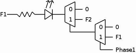
The low side can be reduced to a OR gate that can be implemented with a couple of diodes (on F2 and one phase1). The Shottky's drop requires a specific series resistor value. However the MUX2 can also implement a OR gate. In other words...
![]()
More accurately:
- high side=1 when /CE=0 and (W/Y)F1=1 {else 0}
- low side=1 (to clear the segment for the code 6) when (W)F1=1 and (X)F2=1 and ph1=1
Ooops that's AND3...
Wait
The MUX2 on the left is useless because F1 is floating when /CE is high. So it's more like :
![]()
(phew, I feared I would have to add another MUX2 gate)
Update 20160704: I've manually checked all the equations from the latest version of the schematics, just in case, and it works.
Value:
0
1         Y
2  W         + Z
3          Y + Z
4      X + Y
5      X +     Z
6  W + X +     Z

Intermediate coding:
W = F1, ph=1 (phase 2)
X = F2, ph=1 (phase 2)
Y = F1, ph=0 (phase 1)
Z = F2, ph=0 (phase 1)

Segment decoders (high side && /low side)
A = F2 &&  ph=0
B = F1 &&  F1 & F2 & ph=1
C = (F1&ph=0)|(F2&ph=1)  && /CE
D = F2 && ph=0
E = F1 && ph=1
F = F2 && ph=1
G = F2 && /CE
In 3 cases, one segment is turned on during both phases:
- segment C for value 4
- segment G for values 5 and 6
But this is not critical and I can proceed to route the rest of the PCB.
DYPLED
a thin LED display in SIP module format, much better than TIL311s to visualise your computer buses
 Yann Guidon / YGDES
 And to be honest, it got on tracks thanks to