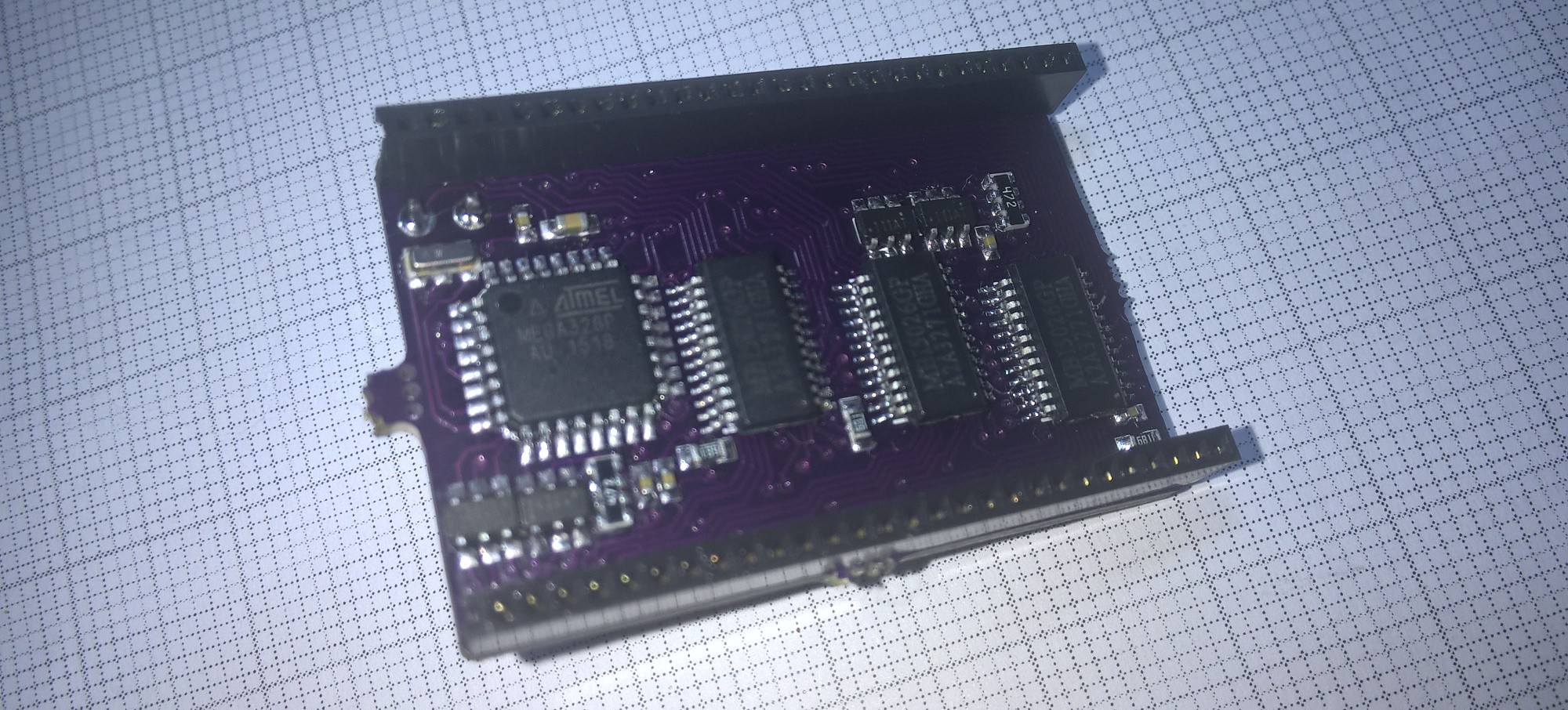
The first PCB is soldered now. Every thing does fit.

During soldering and the later Testing I found some mistakes in the Schematic:
- AVCC of the Atmega should be connected to VCC, because it powers needed IO-pins. I fixed this with a wire
- When using the hardware SPI in Master mode, the MISO pin is always input. But on the PCB it was used as for the latch output. I fixed this by connecting MISO with SDA (both available on a test pad) and using the SDA pin for the Latch output.
For testing I wrote some firmware to sweep through all LEDs. The result can be seen in this little video:Next I will write some more advanced firmware.
 Alex
Alex
Discussions
Become a Hackaday.io Member
Create an account to leave a comment. Already have an account? Log In.
Seems like you were more productive than I was yesterday. I did the usual "getting stupidly drunk" thing and finished the day with watching Star Trek Voyager :) happy post-man's-day :D
Are you sure? yes | no
Hey, that's totally concept work for the hoodie, no?
Are you sure? yes | no
well I was walking the streets with some friends and a beer case - no time for hacking, had to make 10km and finish the beer case in 2 1/2 hours. But yes, watching Star Trek is totally valid for counting as research :D especially Voyager, cause I need to get the neutrino fluctuations and the dampening fields for the dilithium matrices right, or otherwise the matter-anti-matter combustion chamber will deflate because of de-alignment of the dilithium crystals.
Are you sure? yes | no