dave
dave-
Downsizing the FPGA
01/18/2016 at 17:05 • 0 commentsHaving got this far, and looking at the statistics in Xilinx ISE which showed I was using about 1% of the 1200K gate chip on the Nexys 2 board I decided to try a bit of downsizing. I ordered an WaveShare Open3S250E board:-
http://www.waveshare.com/product/fpga-tools/xilinx/xilinx-boards/open3s250e-standard.htm
which at around $35 is rather cheaper that the board I was originally using. Like the Nexys 2 board this has a Xilynx Spartan 3E chip, albeit a much smaller one with only 200K equivalent gates, and an EEPROM to store the configuration. Unlike the Nexys 2 its a pretty bare board with 4-Leds, a mini joystick and a buzzer. It also lacks an on-board USB programmer but as that is also around $35 from the same place and can be used for many other projects it seemed worth a punt. I also ordered a VGA adpator for it @ $4...
http://www.waveshare.com/product/modules/misc/vga-ps2-board.htm
So I was ready to go. As almost all the outputs are brought out onto standard connectors, I also calculated I could remove the SPI expanders and connect the Typewriter buttons directly into the system, freeing the expander boards for my next project.
Getting the basic CPU working initally was very quick. The existing code required only changes to the I/O pin mapping and a couple of tweaks to stop un-connected buttons randomly clearing memory to get to the stage where the basic slider ran. After about a week of fiddling its now all running on the new board with the typewriter buttons connected and all the funcionality working. I now use the "L-Stat" switches on the front to choose which program is loaded when the "Load" button is pressed, but I am now really please with the machine. Next step is to clean up the VHDL for the smaller FPGA an who knows some one else might build one...
-
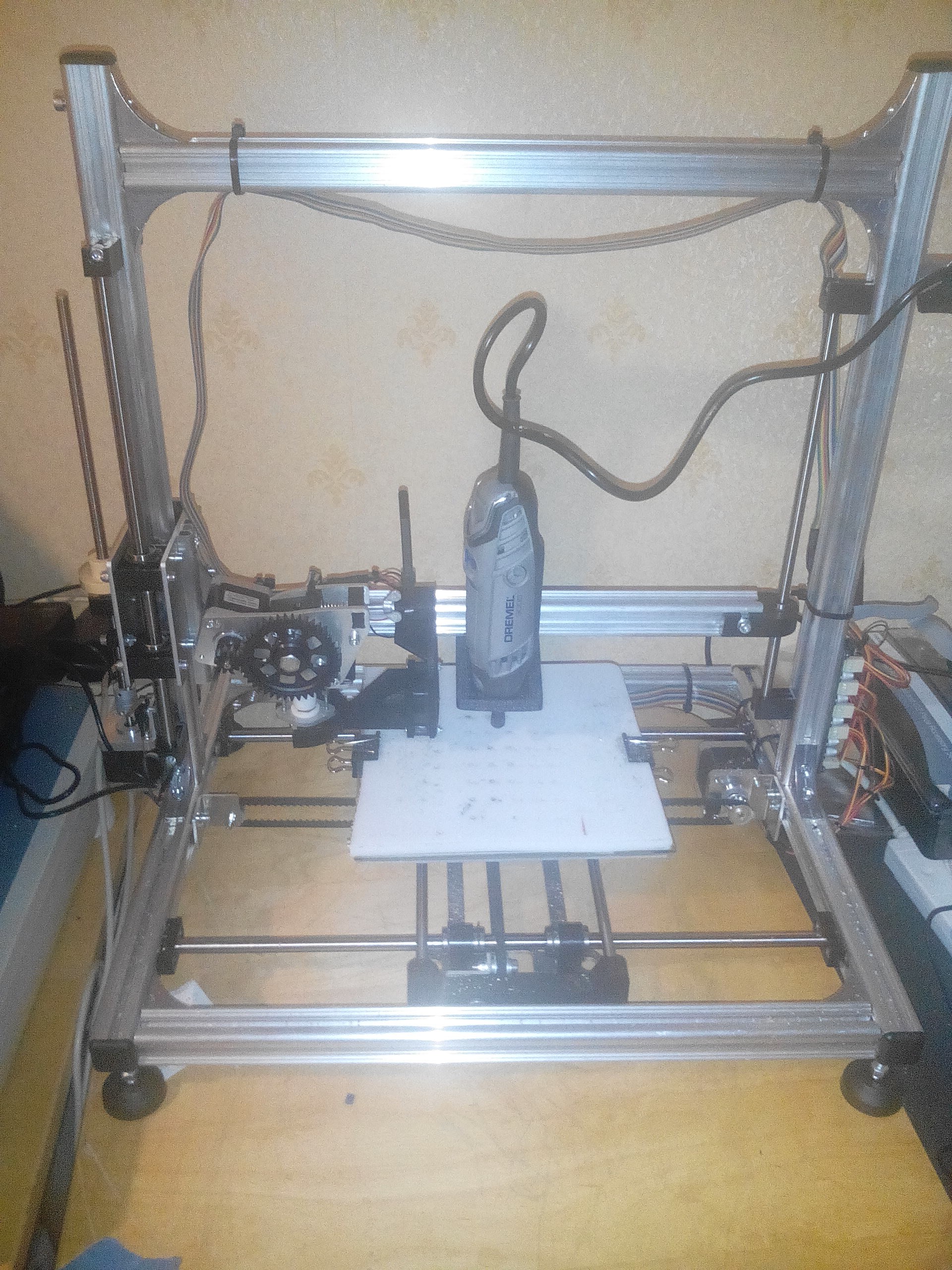
The Frame
01/18/2016 at 16:30 • 0 commentsThe frame was pretty straight forward to make. I used Aluminium Angle and "U" pieces from my locat DIY store. I found that the usual "cross-head" screws looked out of place, but I found some Pan Head on E-Bay which are closed in look-and-feel. I also sourced some Hex-Head bolts to hold the feet in place, again as these look morelike the originals. They are Metric but its not meant to be fine scale.
The small VGA display was also sourced from E-Bat. I think its meant for use in a car but it has VGA and two composite inputs (I guess for reversing camers) and runs off 12Volts. I was hoping to mill the "Trunions" that keep the frame and feet square, but I found that the K8200 just does not have the bed rigidity for real milling. I guess it tyhe next project will be a proper milling machine...
. oh and the stop lamp is a small red LED. The stop hooter is generated on the FPGA and fed into the Audio In on the VGA display.
-
How to mount all those Buttons
01/18/2016 at 16:19 • 2 commentsNow as you can see from the pictures I am not very good at making neat items. In this case I will justify some of the sloppiness by saying “that’s almost how the original looked” but hey its neater than mine. Any way drilling the 40 holes for the typewriter buttons was a challenge.
A quick aside, only 32 of the buttons are used, but they had experimented with different store widths, and the follow on machine, the Manchester Mk1 had a 40-bit store. So at the time it ran its first program it is believed that the Baby had 30 buttons on the Typewriter even though only 32 were used.
Any way back to drilling the holes. My first thought was to make a template from Vero Boards (or other PerfBoard) as these have holes on a 0.1” spacing and so make a great template. However, initial experiments were a total disaster. The vero is so weakened by all the holes it just fell apart as I used it.
Now I do own a Velleman K8200 3-D printer
http://www.velleman.eu/products/view/?id=412554
which is a basically the same as the RepRap 3Drag.
and I know that folks have adapted the model I own to do PCB milling and drilling. It therefore seemed that as all I wanted to do was drill 40 holes it should be a trivial task. The instructions on this modification are here:-
http://www.open-electronics.org/how-to-transform-your-3drag-3d-printer-in-a-cnc-milling-machine/
so I thought great, follow the clues and I can drill the hols like a PCB. If only the world was so simple! The first hurdle was the Proxxon Drill they use. Its available in the UK but is very expensive, and I already owned a Dremel which is a very similar tool. However, the Dremel will not fit in the Proxxon collar. Actually this was the simplest thing to fix. A quick search of the “Thingyverse” turned up a Dremel mount for the K8200:-
http://www.thingiverse.com/thing:388701
and after two or three attempts at printing I had one mounted on my printer….

… then the fun began….
How to tell the printer where to draw the holes? This article: -
http://www.open-electronics.org/3drag-as-a-cnc-milling-machine-creating-g-code-via-eagle-software/
After some investigation I found this tool “CamBam”.
Great I thought, GCODE out, I can feed it straight into the printer. So I sketched up a grid of holes, ran it through the printer, which moved the head around and didn’t drill any holes. What on earth was going on! Time to learn GCODE!
Actually GCODE is pretty simple. Each line has a GCODE function at the start followed by parameters, so
G1 X1 Y1 Z1
Says move the tool head to the point X=1, Y=1, Z1. There is more information here:-
https://en.wikipedia.org/wiki/G-code
Now the problem I had was that CamBam out puts GCODE “G81” which says “drill a hole” and the 3D-Printer does not understand how to drill holes, even with the modified firmware installed. In the end I wrote a small VB program to convert the G81 codes into a series of “G1” codes
So finally I could drill my holes, not all at once, as the print bed isn’t big enough, but he we got it done….
-
How to interface all those buttons!
01/17/2016 at 17:58 • 0 commentsWhilst there are enough inputs on the Spartan3E chip to interface all the switches, on the Nexys 2 board many are only accessible via a "HiRose" connector. Given the small spacing of the pins on this connector, it really needs a PCB to access the connections, and an extra PCB didn't fit with my project aims.
I already had a 16-Switch interface that I had obtained for an IBM1130 FPGA implementation, which uses the MCP23S17 SPI I/O chip, to allow 16 switches to be read via a 4-pin interface. I also had some VHDL that would initialize the chip as a 16-line input device and then continually read the state of 16 switches.
However for the Baby Baby "Typewriter" buttons I needed 32 inputs. Whilst multiple SPI chips can be cascaded on a single interface, doing so usually requires an extra Chip Select line for each cascaded chip. However the MCP23S17 has a nice additional feature. Each chip can have an address set via three address lines. I used this feature to interface the 32 typewriter buttons to the FPGA.
You can see the circuit I used here:-
https://cdn.hackaday.io/files/8912381291008/switches - Schematic.pdf
As you can see its very simple and I just knocked it up on a bit of prototype board. The "pull Down" resistors are mounted on the back of the push button switches. I used a third MCP23S17 to input the L-Stat and F-Stat switches, along with the Manual/Auto, Display Highlight and Read/Write switches. The MCP23S17 chip for these switches was mounted on the same prototype board. So I now had a lot of connections. I needed to make a proper frame and mount all these....
-
The PC Interface
01/11/2016 at 21:44 • 0 commentsAt this point when I reset the Baby Baby it loaded a “Slider” program into main store. This continually moves the data in the bottom 1/3 of the store to the right. If a bit pattern than looks like “text” or a low definition graphics image is stored in this lines it appears to “slide” across the machine. Typically, at MSI a program containing the word “BABY” in those lines is used, although there are others with Boats, Trains and Christmas Trees. I know wanted to test the computer so needed to load additional programs.
When I started on the project my intentions were to write some kind of “Serial Loader” as the Nexys2 board has a serial port on it. However, I am lazy and this would have needed a program producing for the PC, a protocol inventing, and VHDL code writing and testing for the FPGA so I wondered if there was a simpler way that was less work.
I knew that at MOSI the replica can be loaded from a PC. After reading the Baby documentation on the Volunteers web site:-
http://www.cs.man.ac.uk/CCS/SSEM/volunteers/index.html
I decided it might be easier to load programs in the same way as at MOSI. The interface is somewhat ingenious. Williams Tubes are dynamic and so need to be continually refreshed. The PC interface sits in the refresh loop and so over one refresh period sees all the data on the main Store tube. In addition, it can over-write the store by replacing the data as its “refreshed” so on the fly.
It uses a Turbo Pascal program on a Windows/95 PC which interfaces directly to the printer port. The program counts the bits and words as the store is refreshed and if a “download” is in progress it over writes them as needed.
In order to work with this interface, I needed to change the way the clocks were generated in the FPGA. The code at this point generated the “Beats” directly from the 50Mhz FPGA clock, so the only CPU clock signals in the FPGA were the 360 micro-second pulses that it uses to generate each of the four phases of an instruction.
I had to add a 10 micro-second “dot” clock which is the rate at which the Williams tubes are refreshed, and so the rate at which the PC expects to send and receive data. I then used this to generate the 360 microsecond pulses that run control Instruction Execution.
As the data from the PC is synchronised to the Baby Refresh Count I also needed to implement this in the FPGA so it knew where to write data.
Lastly there was an issue with voltage levels. The FPGA is 3.3V and whilst the outputs will drive the TTL in the PC Printer interface, the signals from the PC interface must have 330 Ohm current limiting resisters adding to prevent over load.
After some “hacks” and tweaking of the FPGA code I manged to get the interface working. I tested it using an old Digital VP575 running Windows/95, first reading from the Baby Baby and later writing to it…
.. and after some tweaking I could now load arbitary programs into the Baby Baby…
-
Implementing the CPU
01/02/2016 at 22:37 • 1 commentThe logical architecture of the baby is a 32-bit serial machine with a 100 Khz master clock. In addition to the main Williams tube it has two addition tubes which are used as follows.
- The Accumulator
- used to store the intermediate results of calculations.
- The Control Store
- contains the Program Counter and the Present Instruction, a copy of the instruction being executed.
The instruction format is extremely simple. Only 8 bits of every 32-bit word are used. The lower 5 bits of each word contains a store address, and there is a three-bit op code in the middle. These get copied into two latches, which are called “staticisors” in the documentation. These are known as the “L-Stat” and “F-Stat” in the baby documentation. Obviously a 3-bit op code only allows eight separate instructions, but actually only 7 are used.
The execution of each instruction is divided into four phases which are called “Beats” in the original documentation. Each beat is 36 clock pulses long, 32 correspond to accessing the bits on the face of the Williams Tube during the forward scan, and four to allow the beam to return to the left hand side of the screen. As the beam is suppressed during this period these four beats are known as the “Black Out” period.
The means each beat takes 360 microseconds and each instruction takes 1440 microseconds. I therefore created a waveform with a period of 360 microseconds, but with a highly asymmetric ratio of 320/40 to manage the beats. The four beats are labelled Scan1, Action1, Scan2, Action2. The operations during these phases are as follows: -
- SCAN1
- Increment the program counter.
- Refresh the store
- ACTION1
- Read the next instruction from store and save in the “PI” register
- SCAN2
- Copy the address and function code from the “PI” to the L-Stat and F-Stat
- Refresh the store
- ACTION2
- Execute the instruction
Note that in order for the storage tubes to be refreshed the four phases occur even if the stop/run switch is set to “stop”. Instructions are still fetched, but the stores are never updated.
When I started implementing the CPU I had one design goal, and that was to make it run at the same speed as the real Baby. So in order to implement this in the FPGA I created a master clock with a period of 360 microseconds and a 320/40 on-off ratio derived from the on-board 50Mhz clock. As I was implementing a parallel machine not a serial one, I did not need to replicate the 100Khz clock.
- Accumulator
- Program Counter
- Present Instruction
- L-Stat
- F-Stat
and added VHDL code to mirror the operation of the full sized machine in each of the Phases. As the RAM that represents the main store is dual-ported this code operates independently of the VGA logic. The VHDL code for the CPU takes up just under 100 lines of VHDL, excluding the comments. In order to test the code, I configured the project to pre-load a demonstration program into the memory, connected the Nexys 2 to a standard LCD VGA Monitor and loaded the new logic into the FPGA. Much to my surprise the program ran first time. You can see a video of it running here:-So I now had an operational Baby that would run just one program. I did not even have a stop/run switch. I needed to add the other hardware to make the BabyBaby a close replica of the full sized machine
- The Accumulator
-
VGA - Part II
12/28/2015 at 16:05 • 0 commentsAfter reading the ealier log I realized I left out quite a bit of info on the VGA code. Here is a bit more but you will need to read the code to understand in detail how it works...
When I started this project I had assumed that most FPGA to VGA displays worked like a computer VGA adaptor. I expected to find a suitably sized RAM which was filled with data, which was then read out by line and dot (horizontal) counters which feed the memory.
In practice most FPGA displays do not have a frame buffer. Counters are used to generate the various clocks, but they are also used to select or derive the Video data to be displayed. The logic used in the “BabyBaby” is described below. Although it is peripheral to the main purpose of the machine it is the most complex part of the VHDL code.
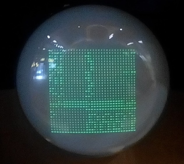
For the BabyBaby I needed to display 32 words of 32 bits giving 1024 bits in total. On the real Baby the CRT scanning circuitry is devised so each scan line on the screen displays one word of Baby memory, with a suitable gap between the lines so they can be observed clearly. It displays a “Dot” for each “Zero” bit in memory and a “Dash” for each for each one bit. A Dash is approximately three times the length of a dash.
This is why the Baby documentation rather naturally uses the term “Line” whereas we in modern computer jargon we would say “Word”.
A quick calculation revealed that I had 640/32 = 20 pixels per bit along the line. I actually used 16 pixels per bit meaning 512 bits/line are used. That meant I could use the lowest 4-bits of the Horizontal Dot Counter to tell me which pixel I was working on. The pixels are used as follows: -
Pixels 0-4 – Always set to “Green”
Pixels 5-11 - Set to “Green” if the bit being displayed is a “1”
Pixels 12-15- Always set to green
That left the vertical spacing’s to work out. The simplest display would of course be to just use one VGA scan line per word, but this looks very thin. If the “Dots” are to be square, as those on the real Baby appear to be then each line must be repeated four times, making a “Dot” 4x4 pixels and a “Dash” 12x4 pixels.
A gap of 8 blank display lines separates each line of data, so each “Word” occupies 12 lines on the VGA display. This is not quite the correct proportion but it fits well on the screen using 384 lines out of the 480 that are available and the visual effect is quite pleasing.
That left how to find the right bit for the right pixel. This is done using a multiplexor. At the start of each line the word to be displayed is read from memory and fed into a multiplexor. The appropriate bit to be displayed is selected by using bits 8 thru 4 of the dot counter and an arbitrary constant so the display appears in the proper horizontal position on the screen. On reflection simply shifting the word might work better and use less logic...
Blank lines are also left at the top of the screen so the vertical position can be set.
This code is I think the most complex part of the BabyBaby…
-
The Store and VGA Display
12/23/2015 at 14:48 • 1 commentWell the Baby proper was really a test bed for Williams and Kilburn's Storage Tube which was the first reliable RAM. This stored 1024 bits of data as 32 lines of 32 bits on the back face of a CRT tube. They built the store first to try and improve early radar displays. When they had the store working they added the rest of the Baby to test it.
There is a description of the store here:-
https://en.wikipedia.org/wiki/Williams_tube
and an article about its development here:-
http://www.cs.man.ac.uk/CCS/res/res02.htm#e
I decided that if developing the memory first was good enough for Williams and Kilburn it would work for me. So I started to create the VHDL code for the memory and VGA display.
On the Baby the CRT that actually stores the data has a wire mesh over its screen that is used to detect how many electrons travel through the screen as the lines of stored data are scanned. Each bit is stored as either a small dot for a zero or a dash for a 1. There is a second CRT called the monitor tube which normally displays the same pattern as the store proper. Here is the Monitor on the real Baby showing one of the demonstration that is run on the replica at the Museum of Science and Industry in Manchester.
The Spartan 3E chip on the Nexys 2 board used in the project includes block RAM which is used as the Baby store. I configured a portion of this as a 32 x 32 bit RAM. This is equivalent to the hidden Kilburn-Williams store CTR on the Baby. The Monitor tube is replaced by a VGA monitor driven from the VGA port included on the Nexys 2 board.
As the CRT needs to be continually refreshed on the Baby the two CRTs run at the same speed. CPU access is interleaved with the refresh so there is never any conflict.
On the BabyBaby the CPU runs at the same speed as the real Baby, but the VGA display of course runs at a different rate. To cater for this the RAM is set in "dual port" mode. This allows the VGA display to access the RAM independently of the CPU.
I would like to say that I carefully laid out the VGA display layout and it all worked fine. However I didn't. The initial calculated layout did not look good, so I tweaked the counters in the FPGA VGA code until it looked OK when displayed on a standard desktop VGA Display.
BabyBaby or Extremely Small Experimental Computer
An FPGA implementation of the Manchester Baby or Small Scale Experimental Computer.