Close
0%
0%

J1772 EV Simulator

An invaluable piece of test equipment for J1772 developers

Similar projects worth following
In developing J1772 EVSEs (charging stations), it's often helpful to analyze the state of the "pilot" line as well as exercise the EVSE by simulating a vehicle requesting state changes. By limiting the simulator to interacting solely with the pilot line, concerns about high voltages can be set aside - the pilot line will swing only a maximum of ±12 volts away from ground.

The pilot signal is a bidirectional signaling line. It's used by the EVSE to indicate that it is ready to provide power, and the maximum amount of current available. It's used by the vehicle to select one of four different states - two of which request power from the EVSE.

The EV Simulator allows you to manipulate the state impedance and measure the frequency, duty cycle and voltage levels of the pilot signal.

The Backpack variant

The J1772 pilot line on the EVSE end is connected to a ±12 volt square wave generator with a 1 kΩ output impedance. The line can either be pinned at +12 volts, -12 volts, or oscillating at 1 kHz with a variable duty cycle. If no vehicle is connected, or if the EVSE is not ready for charging, it will pin the pilot at +12. If the EVSE is in an error condition from which it cannot reasonably recover, it may pin the pilot at -12 volts. If a vehicle is connected and the EVSE is prepared to supply power, it will oscillate the pilot.

On the vehicle end the circuit is quite simple. There is a 2.7 kΩ resistor in series with a diode from the pilot to ground. Most EVs will have a second 1.3 kΩ resistor in parallel with the 2.7 kΩ one, but with a switch (likely a transistor or MOSFET) to bring the 1.3 kΩ additional impedance into play. Because of the host EVSE's 1 kΩ output impedance, 2.7 kΩ will lower the +12 volts to +9 volts. The added 1.3 kΩ will reduce that to +6 volts. Optionally, a fourth state can be defined by adding another 330 Ω, reducing the voltage to +3 volts. This last state indicates to the host EVSE that this vehicle has lead-acid batteries and requires ventilation for charging. EVSEs mounted indoors are supposed to refuse charging when this happens, but EVSEs mounted outdoors can allow it.

The diode will prevent the added impedance from impinging on the negative portion of the square wave. The EVSE is able to detect the minimum and maximum voltage seen on the vehicle side of the 1 kΩ output impedance and therefore detect the state changes. If the negative portion doesn't reach (close to) -12 volts, then the EVSE can surmise that the diode is missing and that a compliant vehicle is not connected and refuse to charge.

The duty cycle of the 1 kHz square wave indicates the ampacity of the EVSE from 6 amps to 80 amps. Additionally, a special duty cycle can be used to indicate "digital communications required," which is what CCS HVDC EVSEs use.

The EV Sim uses a resistor divider network to rescale the potential input voltage range of -12 to +12 to 0-5 volts. Because the impedance on the input side is 200 kΩ, we must provide an impedance buffer amp (that is an op amp configured for unity gain) in front of the analog input pin on the controller. Not doing that results in the previous voltage of the ADC sample-and-hold cap dragging the scaled voltage away for a few microseconds while the cap charges/discharges to the new level. This is brief, but it's still potentially enough to trigger the analog comparator, which results in weird duty cycle aberrations. The controller is also fed a comparison voltage that represents (near) 0 volts on the pilot line. The controller's analog comparator will output a low or high logic level based on this comparison, which essentially means that the pilot is above or below 0 volts. This comparison is used to trigger an interrupt in the firmware and to capture the value of a free-running timer. The number of times this interrupt occurs during a given sampling period is double the frequency over that period, and the difference between the capture and the previous capture allows the ISR to keep a running timing that represents the duty cycle of the wave. During the sampling period, the controller samples the input voltage repeatedly and captures the maximum and minimum voltage. The EV Sim is a "backpack" board on a 2x16 80x36 mm LCD character display. It will display the frequency and duty cycle of the pilot (if it's oscillating) and translate that into a J1772 ampacity indication. Pressing the button will change it into a mode where it displays the minimum and maximum voltage.

The Remote Variant

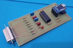
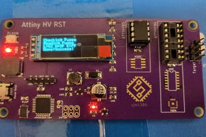
There's a second version of the project that exchanges the LCD for a USB connection. The ATTiny84A is replaced with an ATTiny841, which has a USART in it to make serial I/O easier. The serial pins...

Read more »

EV_Sim_Backpack_4_2_1.pdf

Adobe Portable Document Format - 39.99 kB - 10/16/2021 at 03:26

Preview

EV_Sim_Backpack_4_2_1.sch

sch - 257.49 kB - 10/16/2021 at 03:26

Download

EV_Sim_Backpack_4_2_1.brd

brd - 87.73 kB - 10/16/2021 at 03:26

Download

EV_Sim_remote_v2_2_1.pdf

Adobe Portable Document Format - 50.88 kB - 10/16/2021 at 03:27

Preview

EV_Sim_remote_v2_2_1.sch

sch - 230.19 kB - 10/16/2021 at 03:27

Download

View all 6 files

  • Some software improvements

    Nick Sayer08/20/2021 at 20:22 0 comments

    One thing that can happen is that USB voltages can vary quite a bit. Given that we're scaling a 24 volt range into a 5 volt range for the ADC, even a half a volt difference in reference means a 10% error in the voltmeter readings.

    We can calibrate the reference voltage by comparing it to the ATTiny's internal bandgap reference of 1.1v. Measure that with the ADC and you can indirectly measure the reference voltage. With that, we can scale the ADC readings against our measured reference voltage and make the voltmeter readings a bit more accurate.

    Additionally, if we set one of the timers to free-run and trigger timer capture with the AC output, we can actually measure the duty cycle against the system clock with a very high (16 MHz) granularity. We can also count the number of times the AC output changed during the sampling period to perform the frequency counting, as before.

    With these two improvements, plus the impedance buffer hardware change, the whole system has been pretty much perfected.

  • Yet another issue

    Nick Sayer08/13/2021 at 02:23 0 comments

    Well, I thought I had solved the previous issue nicely by adding a near-zero volt reference and using the analog comparator. Alas, we're not completely out of the woods.

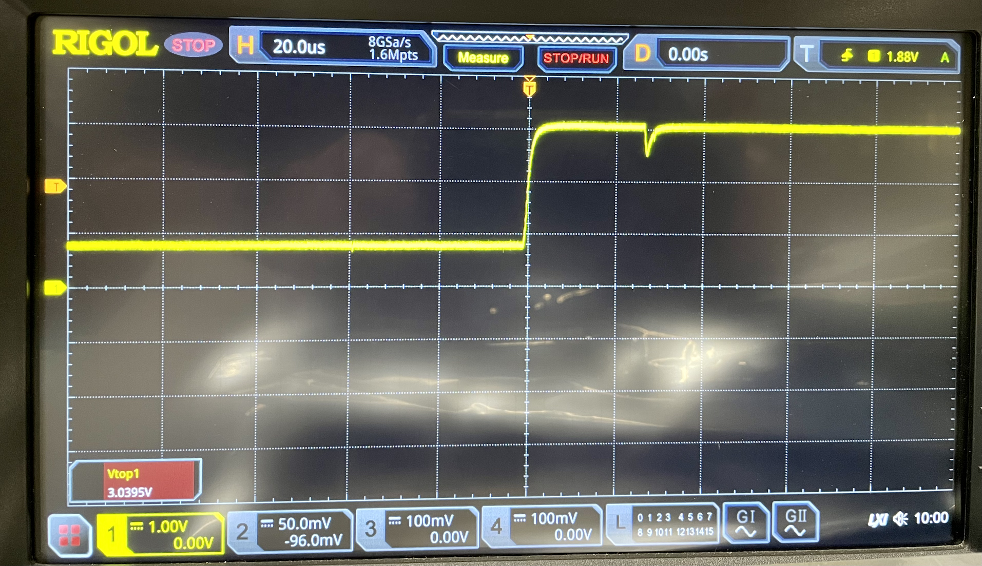
    Here's a view of the ADC input pin with the sim in state D:

    That little 0.5V downward tick is caused by the ADC sample-and-hold. The issue is that the impedance of the divider network is quite high, and the datasheet recommends no higher than 10 kΩ of output impedance into the ADC. That 3 volt level (coincidently) represents a 3 volt input. Dropping a half volt from that drops the ADC sample voltage down to 2.5 volts, which is the reference for the analog comparator. The result is screwy duty cycle readings.

    It's probably adequate to work around this by simply reducing the reference voltage, The little downward ticks don't really have any ill effect beyond this. Another solution would be to add an op amp impedance buffer. I'll probably build a board to see what that looks like, but for now I suspect I'll lower the reference voltage just a little bit.

    EDIT: I lifted the analog input pin and tacked in a GP SOT23-5 op amp wired as a buffer. With that, the effects of the high impedance on the ADC disappeared and it works perfectly.

    I have some inventory of the boards without the amp footprint and will go ahead and use those up with a slightly lower-than-zero AC reference input, but with the op amp I think it's essentially perfect.

    EDIT #2:

    The correct voltage divider for the AC is 10kΩ high and 12kΩ low. With a 5 volt Vcc, that results in 2.71V, which is very close to an input side voltage of 0V. Swapping those two results in 2.27V, which represents -3V, but is low enough to work around the "ticks" seen above. While lowering the AC comparison like that is somewhat less than perfectly accurate, it won't do any harm when working with compliant systems, as the expectation is that the negative should stay close to -12 volts. The worst case scenario is that mode D with a missing diode may not hit both sides of the comparator, but that's two unlikely circumstances (missing diode and mode D) happening simultaneously.

  • An issue has come up

    Nick Sayer07/21/2021 at 05:30 0 comments

    Unfortunately, a small issue has been brought to my attention. When the duty cycle is either very low or very high, the frequency measurement may be incorrect. This happens when the duty cycle is less than about 12% or greater than about 88%.

    It takes about 128 microseconds to perform an ADC conversion. Since the frequency is 1 kHz, that means one whole cycle is 1000 microseconds. 12.8% of that is... 128 microseconds. That means that any duty cycles where the positive-going or negative-going portion is shorter than that might wind up getting skipped over. That means that two transitions won't be counted, and the frequency will read low.

    The fix for this is to configure the analog comparator to be the frequency counter using interrupts. Unfortunately, this can't be done without some changes to the hardware, since the only available internal comparison source is the bandage reference, which equates to an input voltage of something like -10.5, which is way too low. Additionally, for the ATTiny84 (used on the display variant), you can't use the ADC MUX output for the analog comparator while the ADC is enabled.

    The only fix is to free up the two analog comparator pins and provide a reference on the negative input that corresponds to something close to zero volts. As it turns out, this is around 2.75 volts or so, which we can make with a 10kΩ/12kΩ voltage divider. AIN0/00 can be configured as both the positive input to the comparator and the input to the ADC. The ISR can just increment the high, low and change values in the ISR as appropriate.

    We can still perform ADC operations to determine the high and low peak voltage. The ISR of the AC will insure we never miss a transition, and with something like 7000 samples per second, the changes we will miss both the positive and negative edges is minute for any legal J1772 duty cycle.

  • EV Sim Remote build report

    Nick Sayer12/08/2019 at 07:26 0 comments

    The first prototype looks like it may wind up being the final version. It works perfectly (after a handful of firmware fixes).

  • A new iteration

    Nick Sayer11/18/2019 at 02:42 0 comments

    Someone shared with me today that they were using the EV Sim for automated EVSE testing. That inspired me to think of a way to replace the display with a connection to a computer so that interactions and measurements could be automated.

    The result is the EV Sim Remote. It swaps out the ATTIny841 for the ATTiny84. The upgrade gives us a USART for serial I/O. That's connected to a CY7C65213 USB UART and then to a micro USB connector. Instead of the DIP switches, the 3 resistors are switched in and out of the pilot line with N MOSFETs controlled by GPIO pins on the controller.

    The serial port will be set up for 9600 8N1. The output format will be printable and consist of the measured frequency, duty cycle, minimum and maximum voltage. To change state, you simply send an "A", "B", "C" or "D". Unlike the backpack variant, there is no mechanism to remove the diode.

    EDIT:

    Yes, this could be done instead with USBTiny, but then I'd have to make a CDC device and this is just easier.

  • v4.0 now available

    Nick Sayer11/07/2016 at 08:39 0 comments

    The version shipping from the Tindie store is now version 4.0. This version has a button that will switch the display from showing the duty cycle and ampacity to showing the positive and negative peak voltage.

  • v4.0 coming soon

    Nick Sayer01/03/2016 at 22:12 0 comments

    The version of the EV Sim that's in the store today has the comparator, but the one thing the comparator loses is the voltage levels.

    OpenEVSE traditionally uses a three transistor network to sample and scale the ±12 volt range of the pilot to 0-5 volts, and then feeds that into an ADC pin of the controller. However, OpenEVSE has no need to attempt to divine the duty cycle of the pilot (after all, it's the EVSE generating it). I designed the comparator circuit originally because I was unsure that the duty cycle could be reasonably sampled given the extra latency required by the analog to digital conversion.

    It turns out, however, that my fears were unfounded. An EV Sim based on the same sampling circuit works just fine. What you get from doing this is not only the ability to read the duty cycle, but you can also display the minimum and maximum voltages. The v4.0 EV Sim includes a button to switch between multiple display modes - the original one that shows the ampacity, and a new one that shows the minimum and maximum voltage. The voltage readings are not spectacularly accurate, but it's quite convenient, and the duty cycle measurements are just as accurate as it was with the comparator.

    This version will go into the store as soon as stock of the current version runs out.

View all 7 project logs

  • 1
    Assembling the "quick kit"

    First, install all of the through-hole components:

    • The 4 position DIP switch. Install the “on” side towards the top.
    • The pilot screw terminal. Insure the wire openings face out over the edge of the board. 
    • The switch 2 pin header.
    • The blue 2x3 ISP header. Place the notch on the side of the board that has the square pad (pin 1).

    Solder one pin of each, verify that the part is oriented correctly and is flat against the board, then solder the remaining pins

  • 2
    Connecting the display

    Insert a nylon bolt through each hole in the corner of the display from the front. Carefully place the display face-down on your work surface. Position the 16 pin SIP header in the pins on the display (it doesn't matter whether it's the long or short side). DO NOT solder anything yet. Place a standoff over each bolt. Place the control board part-side up over the display, insuring that the bolts go through the matching 4 holes and that the pins of the SIP header protrude through the matching holes. Thread a nut over each bolt and tighten. Once you've verified that the two boards are physically mated together properly, solder each pin of the interconnecting SIP header to both boards.

  • 3
    Power-up and test.

    Power the tester with 6-12 VDC, center-positive. Rotate the contrast pot almost, but not fully, counter-clockwise and adjust for best display contrast.

View all 3 instructions

Enjoy this project?

Share

Discussions

beikeland wrote 09/04/2016 at 17:46 point

Been playing with the idea of replacing swtiches too; ended up with this simulation. Hopefully build circuit soon and test in real life

http://preview.tinyurl.com/hpb7bkg

  Are you sure? yes | no

Evan Allen wrote 01/04/2016 at 15:07 point

I had a thought about this, could a couple FETs be used instead of dip switches and put the display/controls on i2c? I'm basically wondering if that could be used to have a fully code controllable EV simulator, to run through all modes, switch on and off charging, the works.  

  Are you sure? yes | no

Nick Sayer wrote 01/04/2016 at 15:24 point

Well, if you do that, then the "missing diode check" may not work, because the FET itself is going to act like a diode. If you don't care about that, then I don't see why it wouldn't work.

Oh... If your FET has a body diode, then you'll have a permanent missing diode condition. A BJT might be a better choice. 

  Are you sure? yes | no

Evan Allen wrote 01/08/2016 at 19:29 point

that's a good point, or I could just use a relay if I have too much trouble with solid state (but I'd really like to keep it solid state

  Are you sure? yes | no

Martin wrote 11/07/2016 at 12:36 point

You can also use two FETs in anti series or a photoMOS Relais. If the reverse conduction of the solid state switch (in on state) is of no concern, then you could use a (Schottky) diode in series with the FET to block its body diode.

  Are you sure? yes | no

K.C. Lee wrote 01/08/2016 at 20:31 point

You can use a pair of MOSFET connected back to back in series.  This is a very common practice to prevent current flow through body diodes as one of them is always reverse biased.  The issue is that the on resistance is also dependent on the signal voltage you are trying to pass.  (That's why they use both NMOS and PMOS in an analog MUX)

There are also analog MUX... 

  Are you sure? yes | no

Martin wrote 11/07/2016 at 12:38 point

Analog MUX (or switch) like CD4066 are also a good idea, they are available up to 40V and only 10 Ohms. These switches use often lateral FETs with no intrinsic body diode like in CMOS ICs.

  Are you sure? yes | no

Similar Projects

Does this project spark your interest?

Become a member to follow this project and never miss any updates