Spencer
-
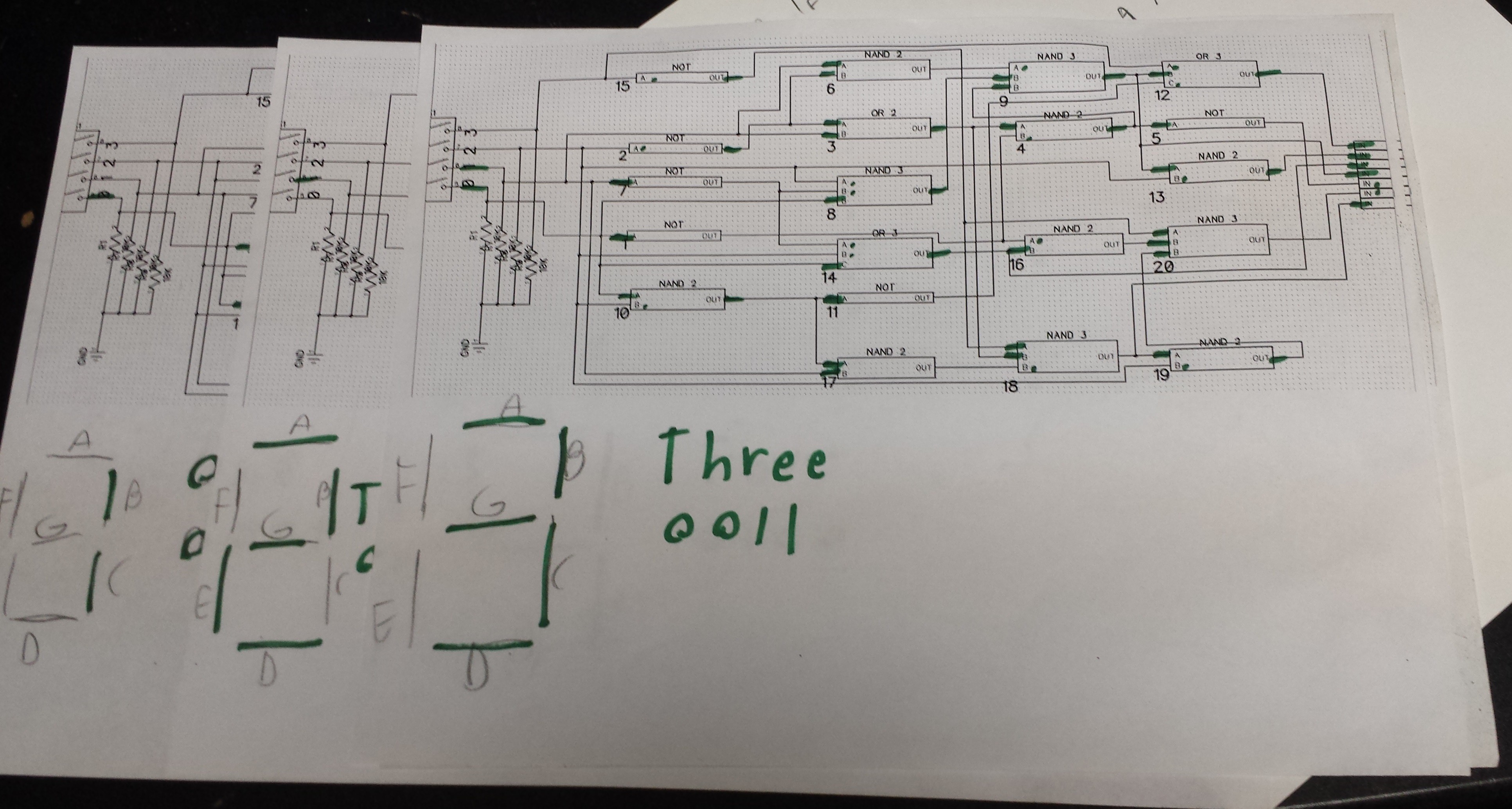
V2 max speed test and V3 considerations
02/21/2016 at 19:34 • 0 commentsPart of the purpose of this project was to act as a testing ground for future projects made out of discrete logic. With this in mind I was curious to find out the max effective speed of the decoder. To test this I attached my function gen to the 8th's position on the input of Bit 3 depending on how you describe it. This produced a path 5 gates long untill the path reached the buffer or F segment driver for the display. I attached my scope to the gate of this transistor and simply feed increasingly high speed signals into it.
I observed some odd 50KHz oscillation on the positive portion of the signal when I drove it at 10Khz. It could be some sort of harmonic effect but the frequency of the noise seemed independent of the input frequency.
![]()
At 50KHz the wave form gets a bit nasty and I deem this the max effective frequency. Currently I am using NAND gates pulled high with a 10K resistor. I'm going to experiment with lower values and see if the max effective speed changes.
![]()
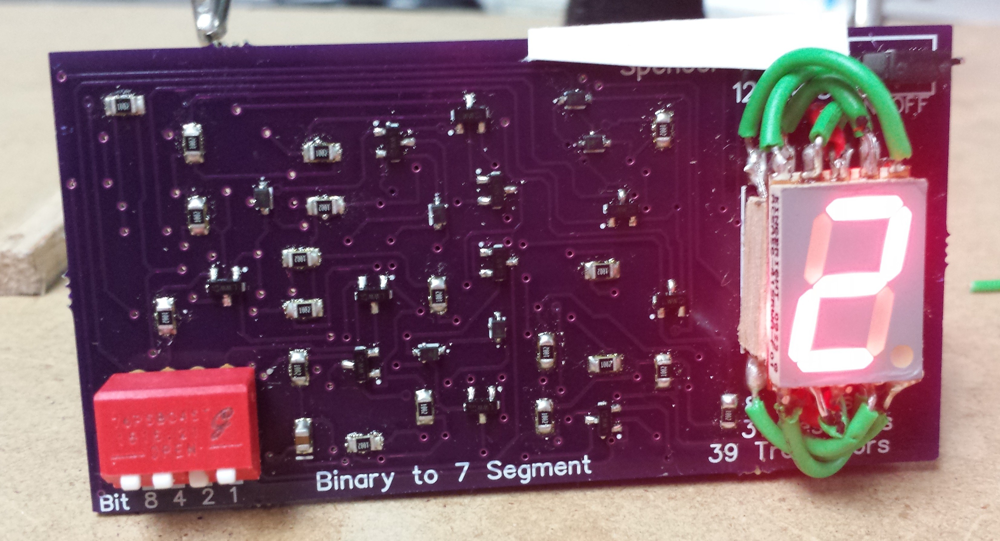
Now on to V3. I never planed to make a 3rd version but I might have a opportunity though my college to make a more educational version. I showed V2 to the professor who teaches the digital logic classes, a class I took and was able to apply to this project. She is interested in a though hole version that ideally will show the individual logic state of each gate. I thought of several ways to accomplish this but I settled on the most reliable option.
I'm simply attaching an LED buffer to each gate. This double the part count but with a board this size, (I esitmate 15-30 inches) I want it to work the first time!
On the left you have the old gate design and the right is the gate plus a buffer. For any one new these are simply 2N3904 BJT transistors.
![]()
![]()
-
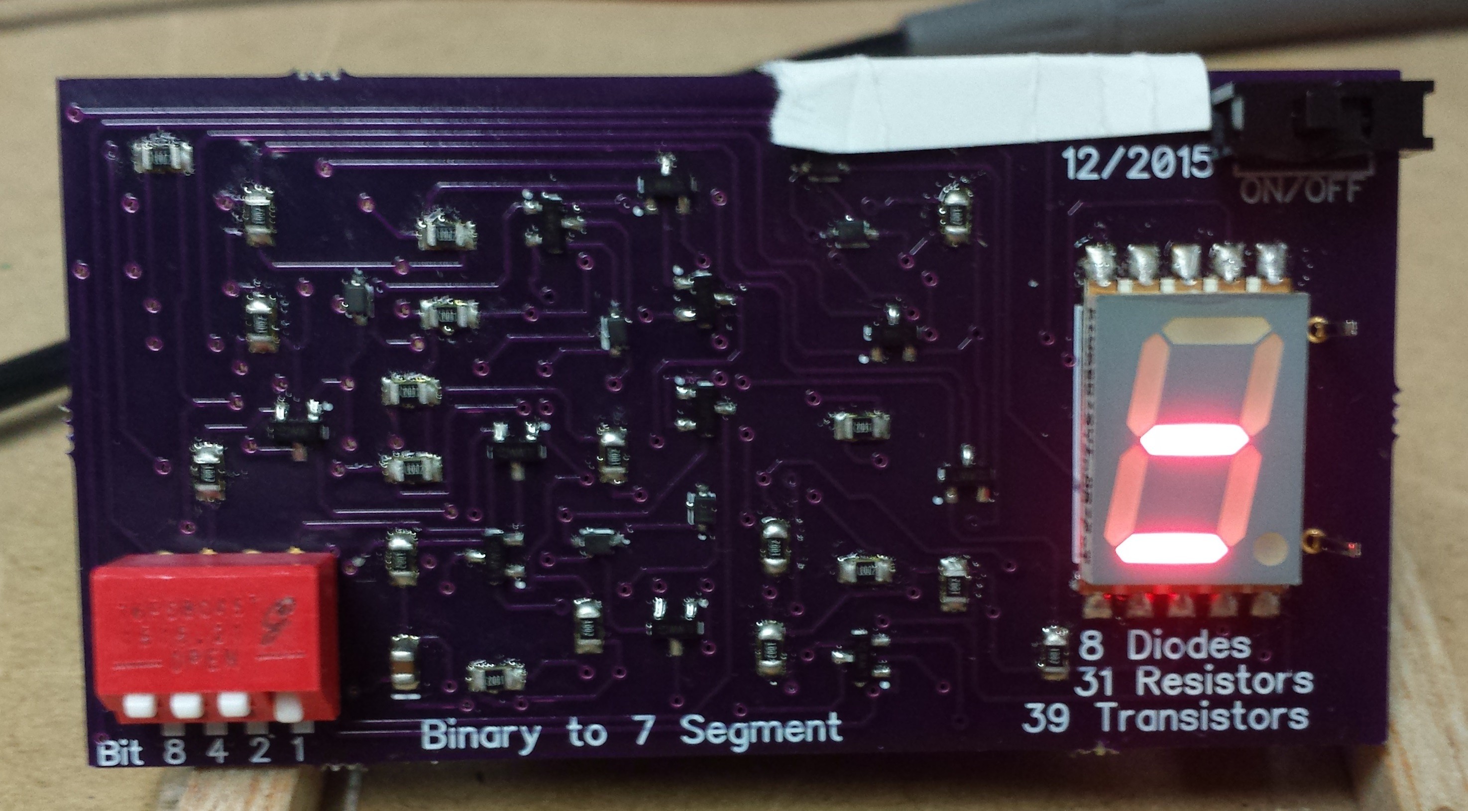
V2 Assembly and fix
01/09/2016 at 23:21 • 2 commentsGetting boards is always a fun event. There's just some thing about holding a board that you designed. Being impatient I got started on it immediately.
![]()
My method of SMD work is sticking the parts down with solder paste (I have a syringe of it I use) and then using a hot air gun to melt it. It's tedious but so far I've always gotten good results with it. I saved the though hole parts for last and I was ready to see if it worked!
![]()
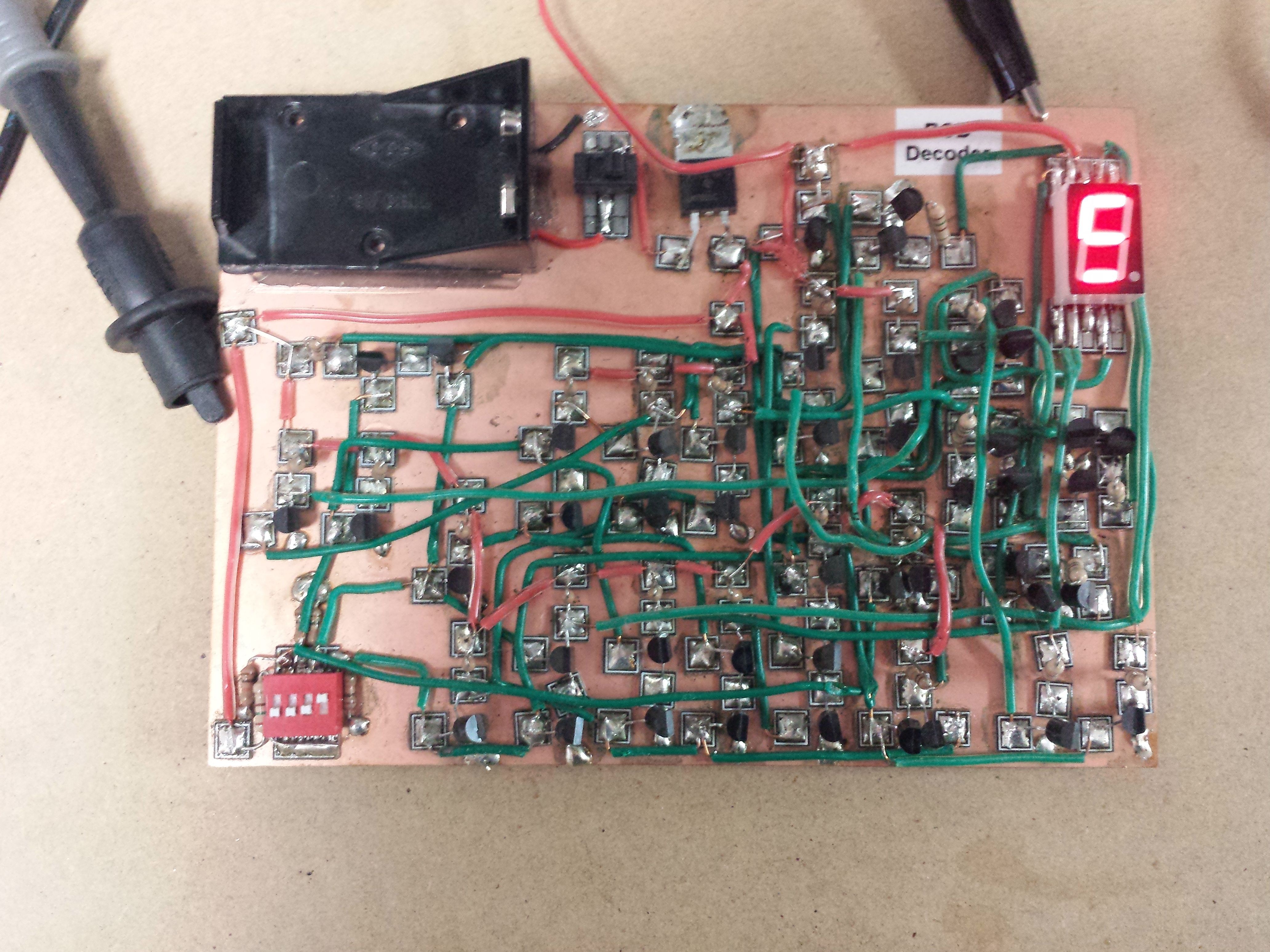
It didn't...... My worst fear was an issue with the core logic circuits and it seems that seemed to be what the issue was. But then I noticed that the decimal point would light up in some positions. I never connected the DP to any thing, left it floating. I went back and reviewed the foot print. Sure enough I had reversed the foot print. Remember kids always triple check your work.This was fixable though and some tedious soldering later it LIVES!
![]()
I did go back and fix the error. All the files on gihub are correct.
-
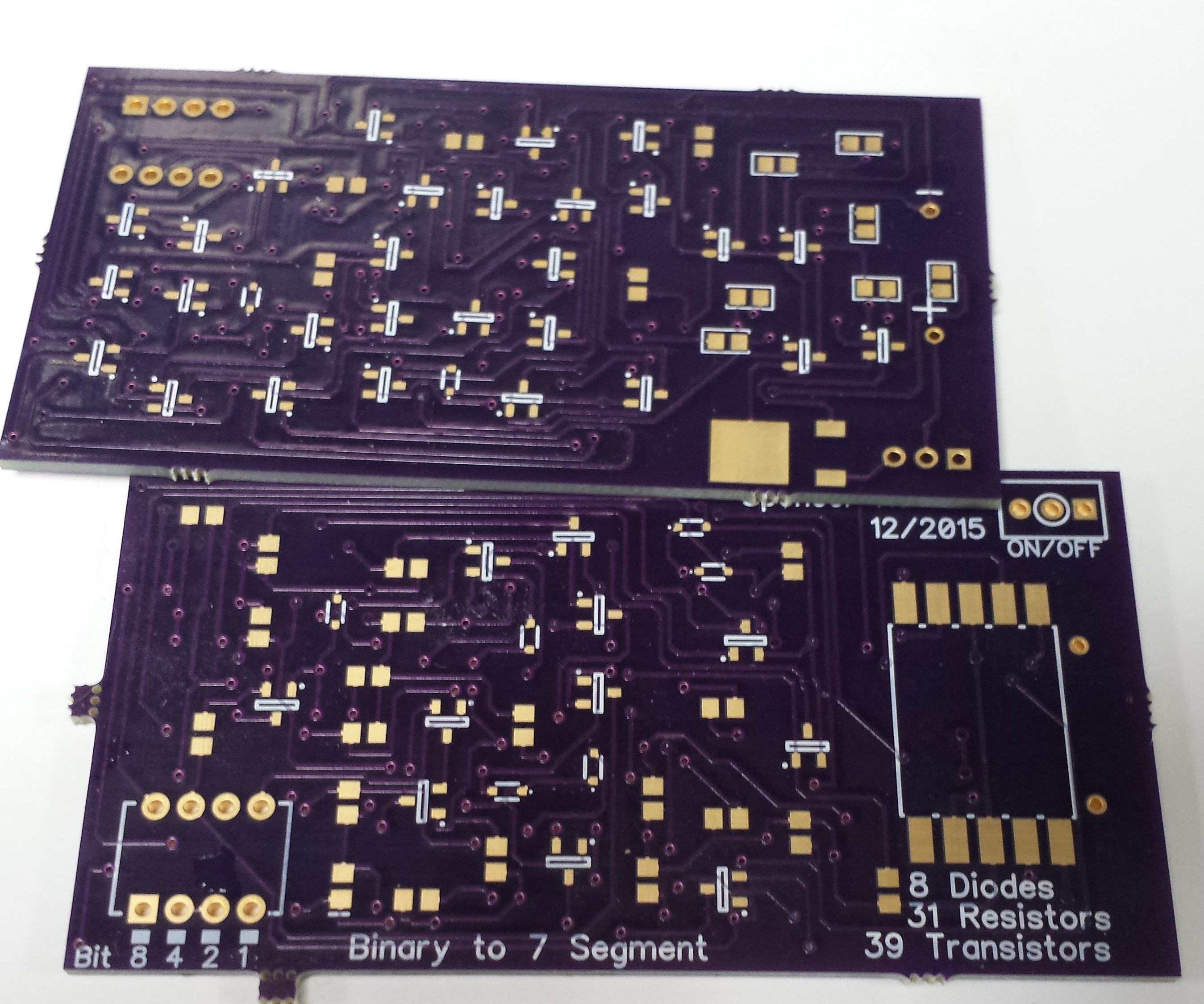
V2 and PCB design
01/09/2016 at 23:00 • 0 commentsWhen V1 failed it was nearly a year before tried again. I redid all the logic design portion as well making liberal use of logic Friday. The file is include in the Git hub. I then recreated the diagram in dip trace. However this time I had a new trick up my sleeve. I figured out how to use hierarchy blocks and was very generous in their usage. This made the schematic a lot cleaner witch for a project this large helps keep mistakes at a minimum.
This time I learned from my mistakes. I printed out the schematic and went though the first few numbers to make sure the out put was as expected.
![]()
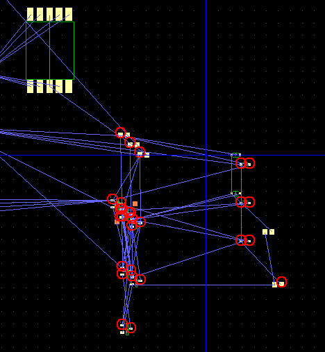
With the knowledge the the core was sound I moved onto the actually PCB portion. I was hoping all the parts would be grouped close to their respective gates but I was massively disappointed. Turns out all the parts were directly on top of each other. As you can see in the picture below there are stacks of fets 2-5 fets deep.
![]()
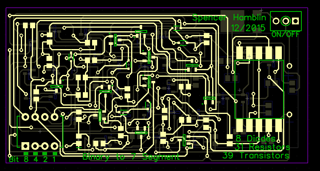
I still took a shot at manually routing it but after getting frustrated I give in to the auto route. Initial results were pretty bad. I played around with it quite a bit but I managed to get it working reasonably well. The resulting PCB was ~5 square inches. I think it would be possible to get is smaller but that is getting close to the limit. The auto router did have to chew on it for a few minutes.
The final result
![]()
-
Version 1 fail
01/09/2016 at 21:43 • 5 commentsV1 was a fail for multiple reasons. For some reason I decided to try to do the project Manhattan style. With the amount of connections and wires I had problems with connections. In addition to that I used cheap Fets from ebay of dubious reliability. What ultimately killed it however was the discovery that my schematic had multiple fundamental flaws.
![]()
Reviewing the schematic
I think this problem arose when I tried to convert it to using a common anode display. I got confused during this process and never discovered my mistake in time.
![]()
V1 trying to display a 1
Discrete Binary to 7 Segment Display
Logic circuit to take a binary input and convert it to a 7 segment display