 Arduino Enigma
The manufactured boards arrive and they are beautiful. Holding in your hand something that prior to this only existed in a computer screen is a nice feeling.
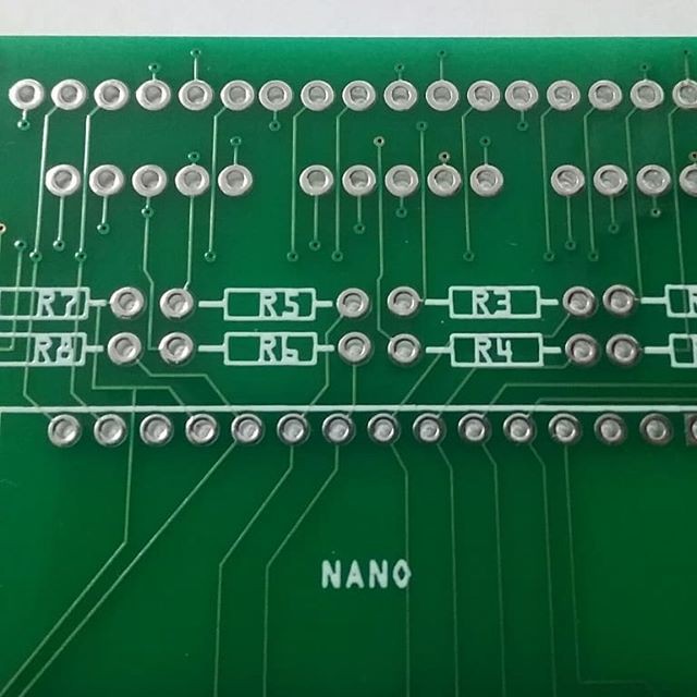
Here is a picture of the front and a comparison to a printout of the prototype from prior log. The footprint for the Arduino Nano is correct, one has been temporarily inserted just to do a test fit.

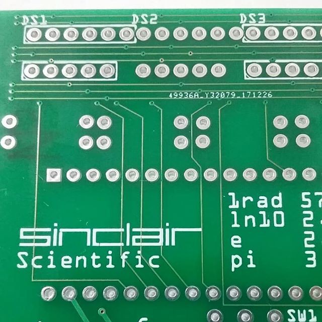
Some details of the front, traces are 8 mil, the fab house has no problem running them in between the solder pads for the Arduino Nano. Next time, we need to pay attention to not running traces through logos in the front of the board.
On the next revision, we need to either relocate the DS1 DS2 and DS3 labels under the display or delete them completely. The manufacturer also added their PCB ID tag in a space between the display bus bars, but since it is outside the display footprint, it will be visible. We need to provide a rectangular area under the displays for the manufacturer to place their board identification number.
The label SW1 on the switch also needs to go under the switch or away. The label 9V needs to be moved to the back, where the power cable will come in.
details of the back:
Today is a good day. Time for a quick instagram post:
Discussions
Become a Hackaday.io Member
Create an account to leave a comment. Already have an account? Log In.