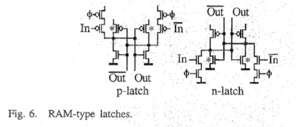
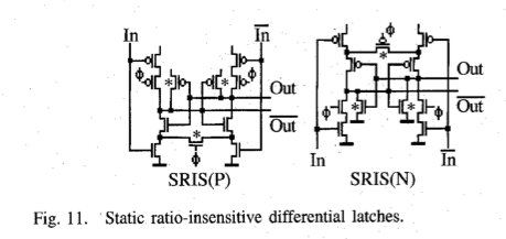
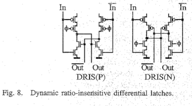
The 10TFF I have designed (or reinvented? who knows!) uses the gate charge as a temporary storage element. This is a known technique in the CMOS ASIC design community (it's called "domino logic") and there is one nice online article about it:
http://lauraknauth.com/academic/DynCMOS.html
Some more similar gates, used in integrated circuits, are found at http://electronics.stackexchange.com/questions/135699/are-all-sequential-circuits-based-on-cross-coupled-nand-or-nor-gates


(I couldn't get the original mentioned paper on the net, thank you paywalls!)
CMOS design has very specific requirements and contrary to the 10TFF (which must be low-transistor-count and low-power, but not high speed),we see that the lach is changed in a complementary way on both sides, while 10TFF is just shorted to ground at one point or another (experiments have shown how slow this is, but it works)
Yet I haven't yet seen an actual design, in papers, books or otherwise, using the precharge of the gate to turn the latch into a true flip-flop.This is what differentiates my 10TFF from the above 3 pictures: I don't just latch ;-)
 Yann Guidon / YGDES
Discussions
Become a Hackaday.io Member
Create an account to leave a comment. Already have an account? Log In.