 Yann Guidon / YGDES
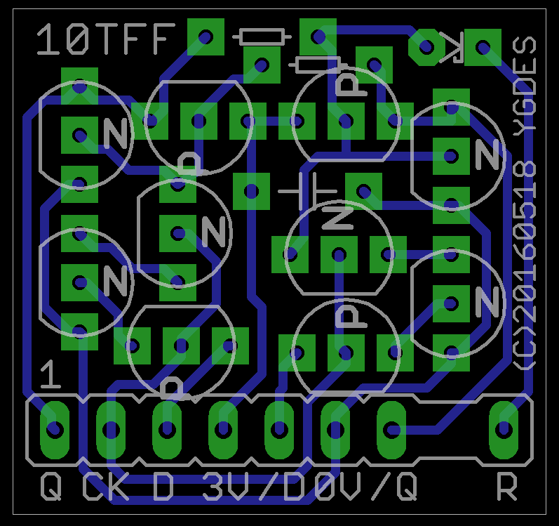
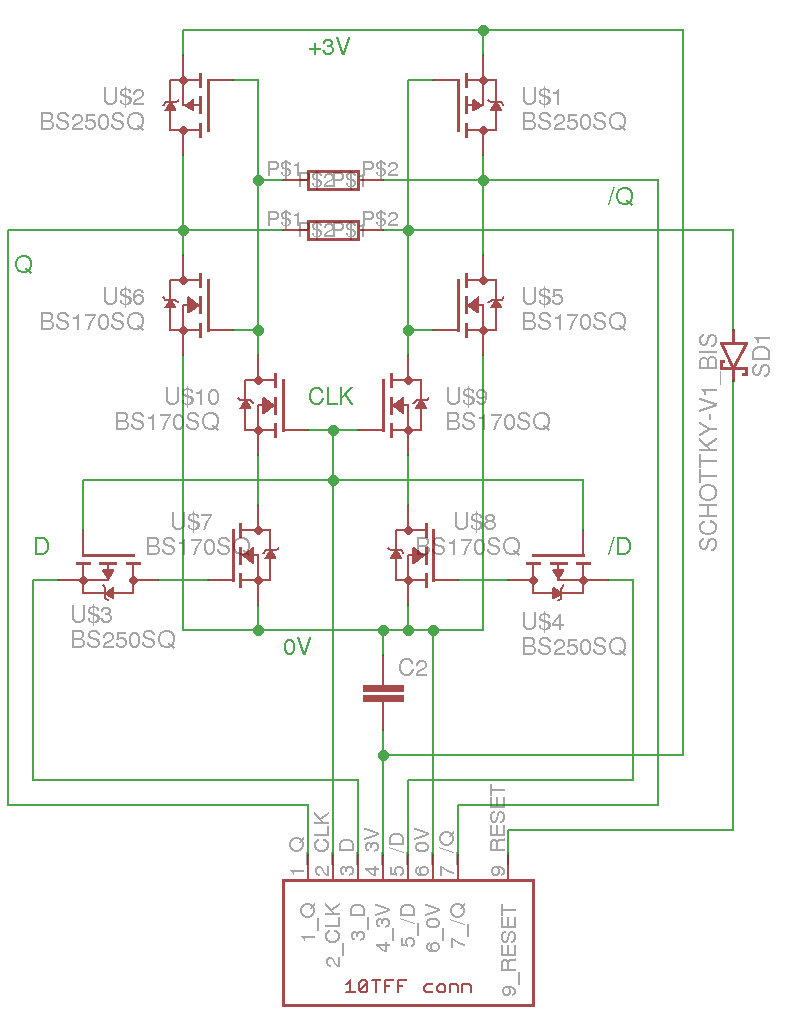
Learning from the mistakes of the first run of PCBs, here is the new layout.
- Added a reset pin
- Added a diode for the reset (marked as Schottky but can be germanium)
- Diode can be soldered in either direction for set or reset function (saving some room on the main board)
- Added a decoupling capacitor
- Added a proper connector (it's now a component in EAGLE so it can be reused to design the main board)
- The connector is keyed to prevent reverse/shifted insertion
- Fixed the drill diameters (the connector can be inserted with no force)
- Changed the pad shape to square for enhanced solderability by beginners
- Pinout compatible with v1
- Still no jumper
- Still 100% single-layer compatible and almost suitable for home etching
- Still fitting in a 25mm square
I've had to play a bit with placement, for example the resistors : they are quite thin so the current placement is not a problem.
I have no idea when I'll be able to afford another PCB run... yes I'm that broke.
Discussions
Become a Hackaday.io Member
Create an account to leave a comment. Already have an account? Log In.