 kodera2t
- Structure
of “Composino”
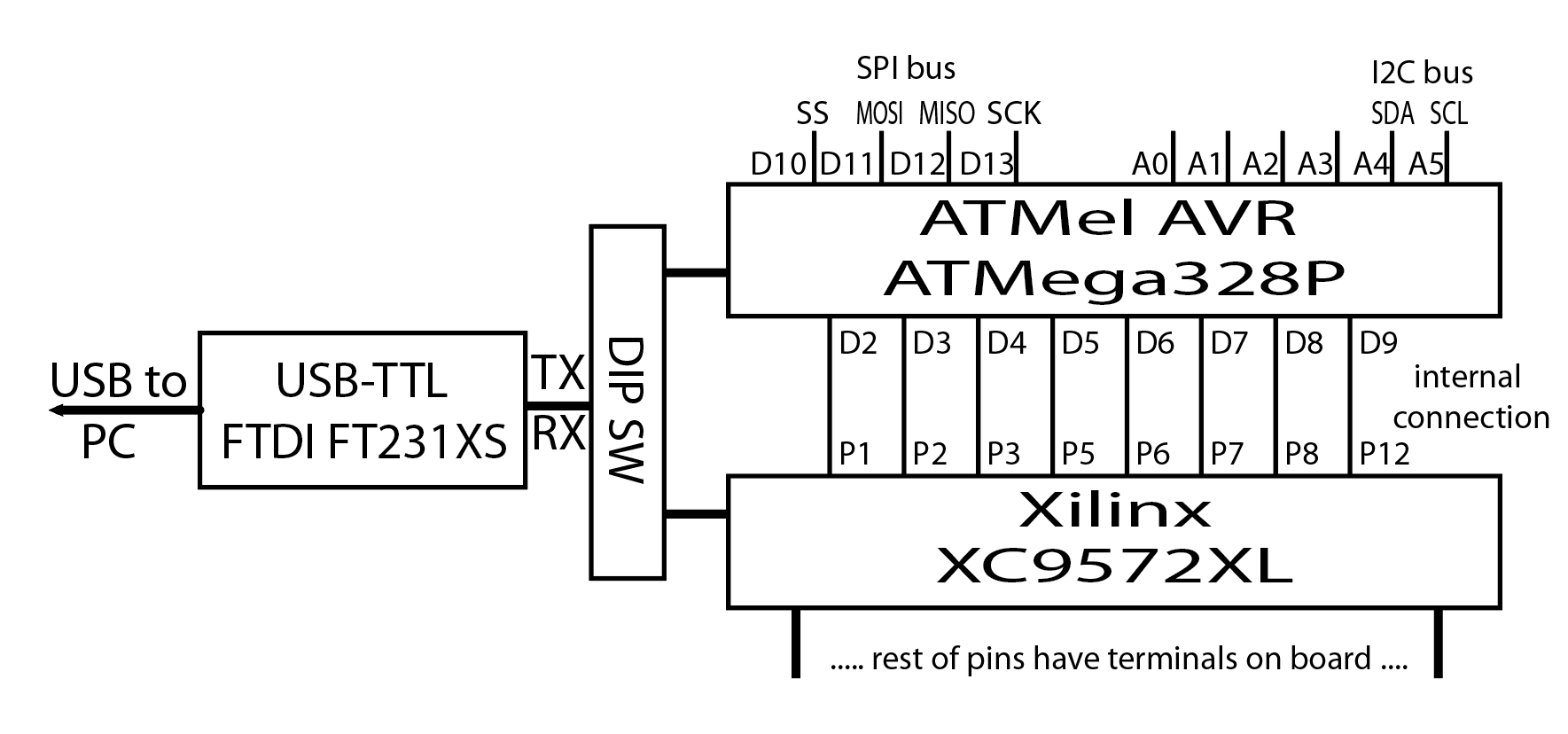
![]() The above
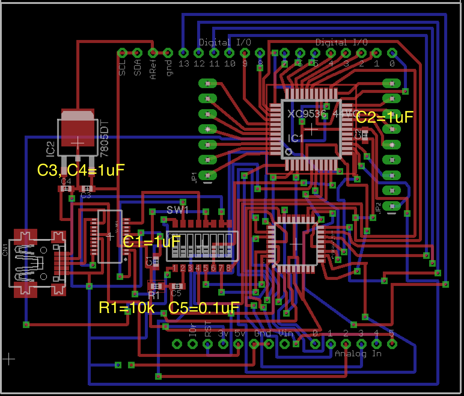
figure shows the configuration of Composino.
D2 to D9 (Arduino naming) of ATMega328P is connected to XC9572XL from P1
to P12. Connecting A/D input to CPLD is not useful and those has direct output.
In addition, SPI and I2C(included in A/D) has direct terminal on board. If some
“SPI design by CPLD” is required, we can just connect D10 to D13 to XC9572XL
pins by jumper wires.
The above
figure shows the configuration of Composino.
D2 to D9 (Arduino naming) of ATMega328P is connected to XC9572XL from P1
to P12. Connecting A/D input to CPLD is not useful and those has direct output.
In addition, SPI and I2C(included in A/D) has direct terminal on board. If some
“SPI design by CPLD” is required, we can just connect D10 to D13 to XC9572XL
pins by jumper wires.
Actually SPI and I2C of ATMega328 is still alive and we gain infinite (limited to CPLD cell size, though) possibility by this wonderful combination. Just to see its fundamental operation, 7-segment driver and counter is made in Composino. (Please note that simple LED segment driver is NOT at most what we can do by this board..) In this confirmation, CPLD part has simple source as follows:
module SEVENSEG(
    input [3:0] SW,
    output reg [7:0] nSEG
    );

always @* begin
	case( SW )
	4'h0: nSEG = 8'b11000000;
	4'h1: nSEG = 8'b11111001;
	4'h2: nSEG = 8'b10100100;
	4'h3: nSEG = 8'b10110000;
	4'h4: nSEG = 8'b10011001;
	4'h5: nSEG = 8'b10010010;
	4'h6: nSEG = 8'b10000010;
	4'h7: nSEG = 8'b11011000;
	4'h8: nSEG = 8'b10000000;
	4'h9: nSEG = 8'b10010000;
	4'ha: nSEG = 8'b10001000;
	4'hb: nSEG = 8'b10000011;
	4'hc: nSEG = 8'b11000110;
	4'hd: nSEG = 8'b10100001;
	4'he: nSEG = 8'b10000110;
	4'hf: nSEG = 8'b10001110;
	default:nSEG=8'bxxxxxxxx;
	endcase
end
endmodule
with following .ucf file
NET "nSEG<0>" LOC="P34";
NET "nSEG<1>" LOC="P33";
NET "nSEG<2>" LOC="P32";
NET "nSEG<3>" LOC="P31";
NET "nSEG<4>" LOC="P30";
NET "nSEG<5>" LOC="P29";
NET "nSEG<6>" LOC="P28";
NET "nSEG<7>" LOC="P27";

NET "SW<0>" LOC="P1";
NET "SW<1>" LOC="P2";
NET "SW<2>" LOC="P3";
NET "SW<3>" LOC="P5";
These source realising 7-segment LED driver, where “P1”, "P2”, “P3” “P5” are binary input and segment out are P27 to P34. As mentioned,P1 to P5 are connected to D2 to D5, and binary number is generated by following Arduino source,
void setup() {
  for(int i=2;i<9;i++){
  pinMode(i, OUTPUT);
  }
}

void loop() {
  byte count;
  boolean a, b, c, d;
  for(count=0; count<17;count++){
    a=count&0b0001;
    b=(count&0b0010)>>1;
    c=(count&0b0100)>>2;
    d=(count&0b1000)>>3;
    digitalWrite(2, a);
    digitalWrite(3, b);
    digitalWrite(4, c);
    digitalWrite(5, d);
    delay(2000);
  }
}
The actual operation can be found in the following movie… Have fun!

 ElectronicABC
 ElectroBoy
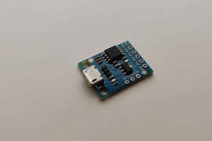
fpga altera ii firmware read and write to another altera max ii. How its possible please suggest all step. Please