 Daniel Frausto
After some research i found a chip ,TI PCM4204, that might be better suited for this project. with 4 inputs and 2 outputs i think it might work a bit better? So I started implementing it in the design.
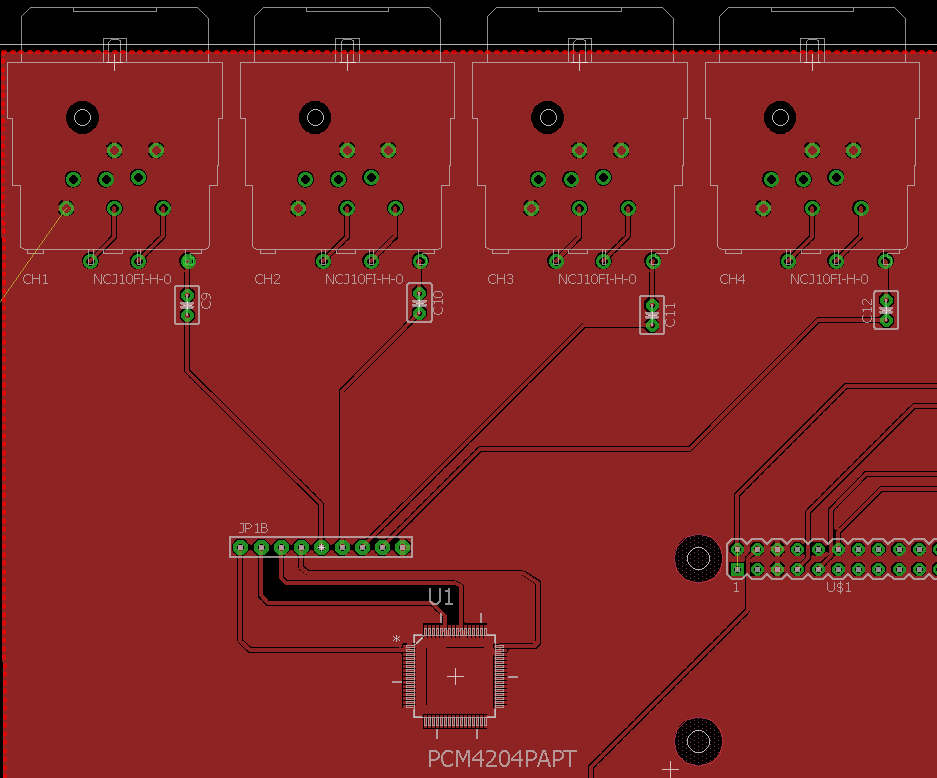
In this picture we can see how the signal goes to pins 5-9 on JP1B then they all go into the faders in next figure.
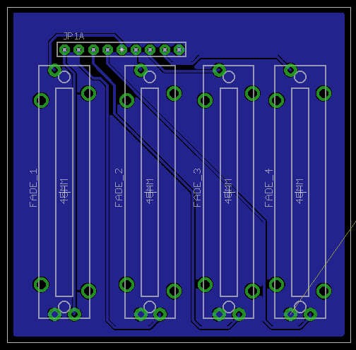
and the outputs again go thru pins 1-4 JP1A and into the PCM4204 chip which will replace the the other chip.
Discussions
Become a Hackaday.io Member
Create an account to leave a comment. Already have an account? Log In.