Michael O'Brien
-
Thermal Performance Woes
06/26/2014 at 18:42 • 2 commentsFurther refinement of the power subsystems are making life easier. I'm tweaking things as the BOM and initial part selection are finalized and slimmed down to reduce the number of unique components and that includes moving to a fixed output LDO for the 3.3V rail, larger copper flows for the 14V LDO and the 5V SMPS.
Previously I have been rating the subsystem to be able to operate at full load when the ambient air temp is 50˚C, aka a little more than 120˚F. This is a bare minimum because though I'm not in Arizona, here in SoCal it is common to get 100˚F days in summer and then some. Anyhow...
With the more regular polygon for the 3.3V rail I can estimate it's surface area and copper volume more accurately. The number comes out to ~13.25 mm^3 split about 45/55 between the back and front copper respectively. Looking up the thermal resistance of a SOT-223, assuming 65˚C/W for the aforementioned surface area seems reasonable. Well, anyhow, since I'm powering it from the 5V rail now, this gives me ~675 mA on the 3.3V rail at 50˚C w/ a T-sub-j of 125˚C.Thermal cutout limit is 150˚C which equates to ~900 mA @ 50˚C ambient temperature.
As for the 14V rail, I'm dealing with a double-edged sword. In order to function without the engine running, I need to boost the voltage input to at least 14.4 V going into the LDO. However, I do not have a way to selectively disable/bypass the charge pump doing this job so I'm stuck with a 18.25-20V input on the 14V LDO when the engine is running. That being said, the surface area I'm presented with for this rail is about 60% the suggested size and would change my performance to about 85˚C/W, which gives me a limit of about 160 mA @ 50˚C with the charge pump enabled and I only need 95 mA. If I get rid of the charge pump though, I'd be able to output ~1.2 amps and it's limit is 1.5 A.
This next bit was something I didn't anticipate. I had previously run numbers for the MPS2209 when it was the 3.3V rail and it was plenty capable of the output desired at the heat levels I needed. However, I forgot to do this when I bumped it to being the 5V rail. Compounding the problem, the 3.3V rail is powered from the 5V rail by an LDO for space reasons. Well, running the numbers puts me at an output current of 520 mA at 25˚C. Though I'm not sure how much the PIC32MX795 will draw when its fully operating but it's rated for 300 mA and I know I'll be utilizing a lot of its architecture. But added to that, the SRAM chip and it's latches are capable of a 280 mA draw.
I have two options if my current draw is too high:
- Switch to a SMPS chip that dissipates heat more efficiently
- Start looking at [SMT] heatsinks
As a patch, the latter is likely, though I'm thinking that I'll have to switch to a different SMPS. If I do that, I'm actually more likely to move the power subsystems off-board. D-DAQ is size sensitive and to keep costs "down" I rather shrink the mainboard. Though ultimately more expensive, moving the power subsystem off-board means that I can dedicate the proper amount of space to heat dissipation for the LDOs and the SMPS. Based on how much time I've spent going over surface area vs thermal dissipation, I estimate this board will be about 2/3rds the size of the mainboard.
Though it's more complex and undesirable to layer two boards on top of each other, it'll simplify power routing on the main board a great deal. Also, two layer boards is more desirable that increasing from a 5cm x 10 cm footprint to a 10 cm x 10 cm footprint. In fact, I'd probably trim the mainboard's width down to about 7 or 8 cm. If I do move to a different SMPS chip, a cursory look on mouser show the MIC24052/24053/24054 or ZSPM4022 as viable alternatives. Each of these chips share identical pinouts and footprints and offer a 28˚C/W juntion-to-ambient rating over the 48˚C/W rating of the MPS2209.
-
Initial Soldering :)
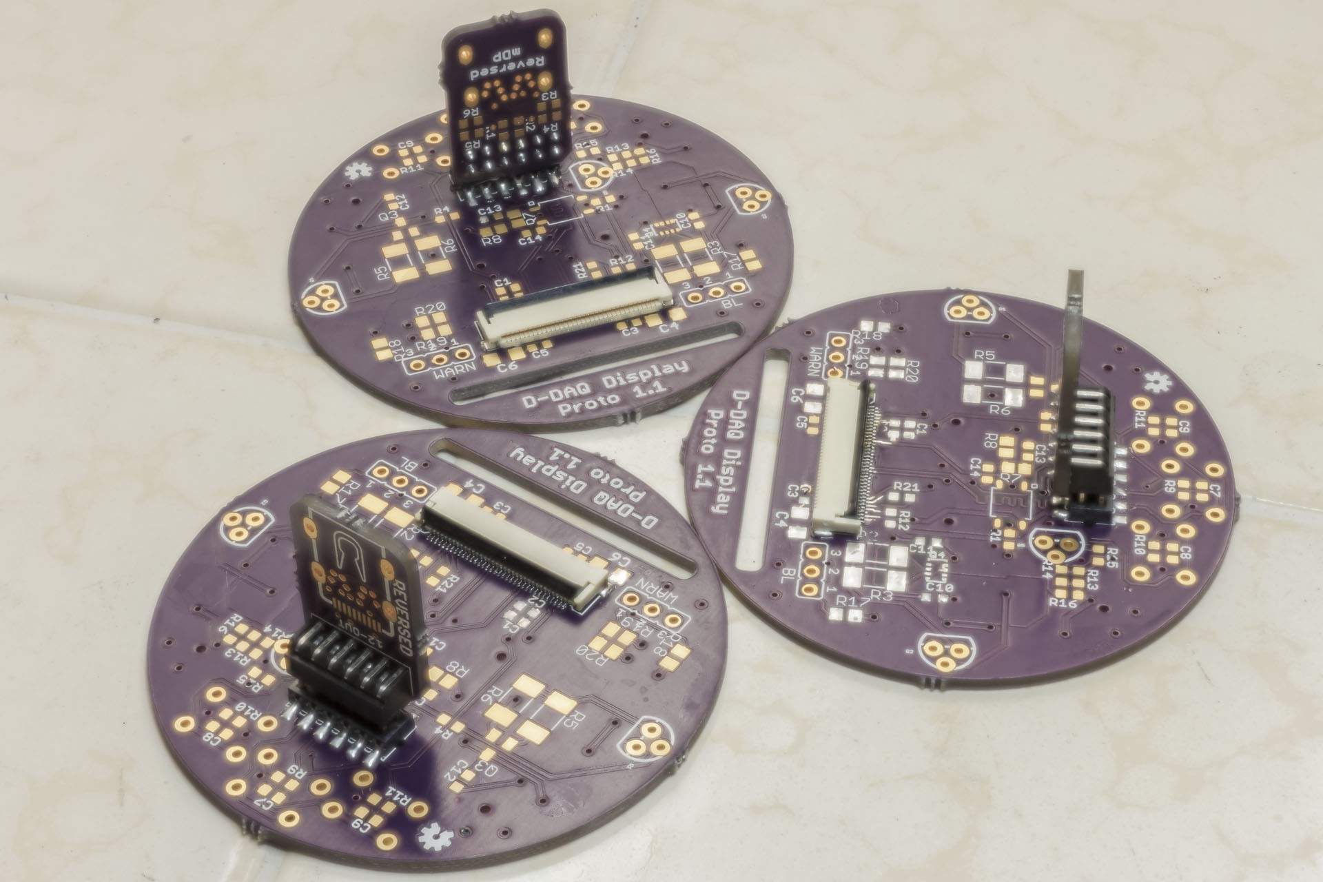
06/26/2014 at 06:53 • 0 commentsHonestly, it's been a few years since I've done some significant solder work. I do have an unfinished, but recent brush up on SMT soldering but yeah. I decided to break out some more heat tolerant parts to get a feel for the hot air rework station and it's iron compared to my old one. Tonight's victims were some interconnect work on the display boards and adapter boards.
![]()
I need to adjust the mDP footprints a little bit to accommodate for the slots, also make the tabs on the 35-pin FPC connector stick out a bit more, and tweak the placement of the slot every so slightly, but I like the layout of the Display Board. After experiencing quite a bit of bridging on the 0.5mm pitch FPC I think I'm comfortable with the iron's and hot air gun's temperature controls, the SAC305 stick solder, and the 63/37 solder paste. I have most active components, a few passives, etc. I *still* need to finish my BOM and order up the remaining parts. I'll still be able to map out an initial order of assembly for soldering the mainboard and display boards. Things are still looking good for starting to code a week from 7 minutes from now!
Side note: Soft focus effect on the photo is unintentional, but resultant of the focus stacking algorithms.
-
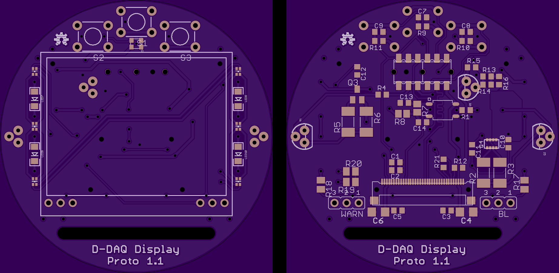
Display Board - Design Notes Part 2
06/14/2014 at 04:41 • 2 commentsIn case you missed it, Part 1 is listed here
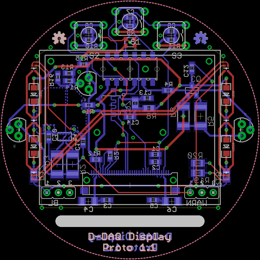
![]()
Aesthetic Function
Next one is a bit of a personal pet peeve. I really enjoy auto dimming when it is implemented correctly. I'm a photographer and I specialize in low light photography. The next thing I need is to have a glaring cell phone screen light up and ruining no less than some night vision. For detecting the amount of light, most use an LDR in a voltage divider network and pass it to an ADC. It works for those simple things, but I am dead set against using any ADC lines for just a backlight control. I needed something more precise and with a logarithmic output so it'd adjust relative to how the human would. This eventually led me to the APDS-9007. It outputs a small amount of current dependent upon how much light hits it, from 3 to 70K lux. Wikipedia, as usual, has a decent article on lux.
A detail about the SEPS525-based displays stuck out to me: They have a resistor valued in the high 60K's to low 70K's tagged onto 2 pins. It's even labeled as a control for internal brightness. Information is lacking about how much current is flowing through the resistor, if it's a constant current source on the other end, if it's a part of a voltage divider, if a greater value increases brightness or decreases it, etc etc. The only way to figure this out would be to test it. Unfortunately I'm dealing with small pitch SMD components so I either make breakout boards and check everything and then make up the prototype, or I build the test circuit into the boards. I chose the latter especially considering I'd need 1 of the 2 resulting circuits, albeit modified, in the final design to have this function.
I'm sure you've figured out that I'm talking about dimming control on the displays by way of the APDS-9007. Using a transistor as gain and coupled with a pair of resistors and switching between a PNP and NPN transistor, I can figure out how this resistor's value affect the OLEDs display brightness and use it to my advantage. Full details are outlined here. In short, I'll have independent and tailored response of the OLED displays without needing user interaction.
Mechanical Design
So, my target size was to get the display to fit inside a 2" gauge pod. Unfortunately this turned out to not exactly be possible. Well, maybe. I need to see if I can have a 2" body and is a 2.25" board dia. is an issue. Now, how did I get to this size? First it was a simple function of the display size. Though the viewable area is only ~1.7", there are conductors and extra glass that add extra size to the OLED display's structure. I have to also fit 3 buttons within proximity of each other on there somewhere too. Since the display is wider than it is tall, the top of bottom would need to be utilized for the buttons.
Buttons. I kinda hate them because they take up so much space for such a mundane task. For a spell, I researched capacitive buttons that way the space behind the screen had some function. The added component list and complexity isn't worth it for this.
I then realized that I had a little problem, the display FPC. There was simply no way to have it plugged in on the same side of the PCB as the display resided. I had to break out the calculator and let it deal with converting mm to mil and pixels to each and back and for etc etc, while I was having to think in 3D space to know where that connector would be on one side of the board and where the display would end of residing and where the graphics would visually end up residing.
From the graphic way up there at the top, you'll notice I have a slot in the board. I came to the conclusion that it is the most elegant solution of running the FPC through the board instead of chopping off the bottom of a circle. I think I have it shuffled appropriately to minimize chaffing and to allow some manufacturer tolerances. It was a few hours of sitting around with a calculator, calipers, a display. and photoshop that I kind wish I could forget.
You'll notice too that the buttons are up on top. Due to the display's FPC I didn't have much of a choice in placement of the buttons. I almost rotated the board upside down for this so your fingers or hands wouldn't cover the display when pushing a button, but it proved to not be desirable. Why? If you had a gauge that was inside a pod and it wasn't centered, how much would it bug you? Well, It'd bug me a bit. With the board rotate 180˚, the placement of the gauge face(s) would be such that their centerline would be around 0.2" lower than centered. The lack of concentricity would easily be seen. Having it right side up, buttons on top, allow the centerline to be less than 0.05" below center of the board.
I have the buttons up and the top, and the center one, the selection button, raised along the perimeter of the board. Below it is the ideally placed light sensor. Now, the other part I've had to tackle is figuring out how to tack the display to the board. I've strategically placed a view vias around to fit into holes of the FPC, act as a shelf for the display, be corner tie downs so it won't fall forward, and to allow some material to be roped though (wire, thin silicone tube) the board and be a cushion behind the display to help protect against vibration. Overall, a little more tedious, but less permanent than glue.
I have the LEDs aligned with the display's viewing area, not the center of the board.I may shuffle them down latter, but if the whole screen has something displayed on it by chance, then I prefer to have the accent and warning lights aligned with that region. Who knows, I may split the difference in the end.
Adapter Boards
Lastly is the 6x2, well two 3x2, female pin header on the board. A mini DisplayPort cable is like most others where they are flexible, but tight spaces are not their friends. Yes, the cable can be bent to fit in such a space if a right angle connector is used on the PCB, but then I'd have less board space to clearance the cable. As perpendicular adaptors are hard to come by, making a simple adapter board proves to be advantageous. Ironically, this also simplifies the board layout in case a different receptacle has to be used so the display baord's pin out stays constant.
This provides me with another unique solution. If my chance my assumption about being able to drive the displays while doing everythign else on the board is wrong, I have a "simple" solution. I can turn the adapter boards into an intermediary. I've had the concern expressed that the displays I'm using might be too small. At the same time, there isn't enough bandwidth to drive a larger display at 60 fps, let alone 3 of them. If I change the design scheme over to sending drawing commands instead of pixel data, then I just need a MCU on the other end of the cable to interpret the drawing commands and draw the display for me. Either way, D-DAQ will meet my design specs even if I have to wait until version 2 to do so.
-
Display Board - Design Notes Part 1
06/14/2014 at 04:38 • 0 commentsI've talked at length about the mainboard for D-DAQ because that is where so much has to go right for anything else to be functional. In order to do something with D-DAQ so it's not a lifeless brick, there needs to be a way to see what's going on (duh!) so that brings me to the displays. So, though I've mentioned some details about these boards, here is the design philosophy behind the boards and why they're a little more complicated than just an adapter.
![]()
Connection
First up is how we get to the displays and that obviously means a physical tether, a cable, unless we're going RF. Come to think of that, it would be kind of awesome for that to happen but I digress. The minimum connections I need are power, ground, SPI Clock, SPI MOSI, and 1 line to toggle between commands and data. In fact, you could almost use a standard USB cable with this though due to other design considerations, I need a few more connections.
D-DAQ is capable of 16 inputs, albeit 2 are digital and may not need to be visually monitors. Even on 3 displays, this is still a bit of info and especially so when the design scheme, a gauge, means that at least 1 piece of info is largely dominant on the screen. So, 14-16 inputs on 3 displays? How do you figure out what goes where? Do I dictate that or let the user decide? Who here has a product that your interaction is dictated by the manufacturer in a frustrating and non-intuitive way? Yeah, I'm trying to avoid that, but nothing will ever be perfect. Anyhow, this brings me to the point where I need some sort of user interaction so buttons are getting tossed into the mix.
If time and space were not a concern, I'd mux the buttons and send them over the MISO line back to the PIC32 on D-DAQ. However, I don't have the space for such an encoder at the time. A basic UI needs at least 3 buttons to walk through it and then some very intelligent design to minimize frustrations. I'm adding on 3 more connections required for the buttons.
One detail that I nearly overlooked is whether or not a display is plugged in. This is commonly referred to as Hot Plug Detect[ion]. Pull a pin high or low, it matters not. It's just nice to know if I'm sending data to a display on the other end or not ;)/ Add 1 more connection.
Indication
Next up, this stems from the idea of being a gauge. A gauge tells you about a physical aspect of, well anything, the device under operation. What happens if all of a sudden this physical aspect goes beyond it's acceptable parameters? I love the OLED screen because each pixel emits it's own light. Though this is advantageous, they usually are not bright enough for illumination, just indication. I could go with sound, but who here likes the door chime in their car when you leave a door open or headlights on (intentionally). Besides, speakers are big, even piezos, and they need some additional circuity for driving and the modulated signal for a tone, etc, etc. This is ignoring the fact that our eyes have better spacial acuity than out ears. Well, that leaves the good 'ole LED for a warning light. I don't like the fact of just 1 degree of warning because with physical devices, there is a zone where you're stressing the device, but not at a threshold. I happen to find the perfect 1 chip, 2-color LED that outputs red and yellow; perfect!
Aesthetics
Well, while I'm on light(ing), I figure that there will be some people who want to integrate this into their vehicle with some semblance of it looking or matching the stock appearance. I know this is a particular desire for the 4th gen Volkswagen Jetta owners. The blue on their dashboard is indigo, which is not quite blue, but not quite violet. From looking around online, this comes out to a wavelength of about 430 nm. Though I'm not catering D-DAQ to one particular manufacturer, let along a model or generation, I am still paying homage to the community from which this idea first existed and where I've drawn inspiration from. As such, indigo accent LEDs are on the PCB. In fact the layout supports any pair of LED that sports a series forward voltage below 13 V. This is basically any red, yellow, blue, green, cyan, magenta, etc LED you can shake your fist at. The display board can be adjusted relatively easily by a resistor change and, if needed, a package footprint change as the indigo LED is on a 1206 (US) footprint.
Lighting Control
LEDs are amazing little devices, but they vary in brightness and current draw heavily. Some are too dim to be seen when in direct sunlight while others are blinding. On top of that there are various control methods utilized for adjusting their brightness. I have native PWM on the PIC32 I'm using so I figure I might as well put it to use. Though it's not able to source enough voltage to drive a single LED while doing the multitudes of other operations, the PWM signal is strong enough to control a MOSFET to sink more power into the LEDs with short duty cycles. Since the Warning and Accent LEDs are functionally different, they need separate control lines. Add 2 more to the mix.
As I mentioned a short while ago, the I have a nice high(er) voltage rail I'm using to power the LEDs. Now I could just run a 14V line up the the display board and a 3.3V line for logic, but having individual regulators, linear or SMPS, on board will just create expense and headache and heat that will hinder development. This is why I had to do a bit of an overhaul on the power subsystem of the 3rd prototype. Despite that headache, it's simpler and less costly to have 1, 14V source and feed it to the displays, imho. Tack on an addition power line.
Now, reason would have it that for a specialized device, being pretty distracts from danger. As such, I have to make it so when the Accent LEDs are on, the Warning LEDs are off and vise versa. This is convenient too as it reduces power consumption ;). Well, before I found out I have extra control pins, I had to come up with a clever solution to this. This is why it's tricky:
Though the Warning LEDs are single chips, they are 2 LEDs. I've decided to utilize the duty cycle of the PWM wave and use a P-channel MOSFET complimented by an N-Channel MOSFET, both on the same IC too, to accomplish this and not need 2 PWM lines for this single feature. I'd also need to turn this circuit on or off and due to the MOSFETs I'm using the only reliable way to do this is to actually cut the power power. I'd need an additional control pin for that and I don't have any.
Well a PWM signal can be passed into an RC circuit to get a rough analog voltage. Using a 2nd order filter smooths that our considerably though. I happen to be using some SSRs (solid state relays) on D-DAQ's main board for similar control. Using a Normally Closed SSR that is driven by the output of a RC filter on the Accent light LEDs means that there will be no power for the warning LEDs. I tuned the filter to turn on at approximately 10% brightness output of the Accent lights so there should be plenty of distinction between the two sets of LEDs.
Separately I'd need another control line. Through limitations and designing around them, I don't need a 3rd PWM line or additional control lines. So, even if I've not talked on them specifically, I need the following lines to have a functional display board:
- Ground
- 3.3V Power
- 14V Power
- SPI Clock
- SPI MOSI
- RS Toggle for changing the display between Command and Data
- Buttons 1 to 3
- PWM for Warning LEDs
- PWM for Accent LEDs
This tallies to 11 conductors that I need in a cable. I could run 3 USB cables, use custom ribbon cables, or find a high count, production cable. Mini DisplayPort was opted for due to size, royalty free use, and pin count. It beat out micro HDMI because a mDP to mDP is a standard cable but micro HDMI to micro HDMI is not. Though there are technically 14 conductors available, I thought it wise to keep the outer most SMD pins unused so I have more receptacle options and avoid shorting out the board, just in case ;). If the will of the people will have it, and this project becomes desirable for purchase, I'll spend the time to rework the mainboard's layout to utilize those 3 extra pins I have and remove the 2nd order RC filter that controls the Warning LEDs. I have that 1 pin open ;).
-
More On the Way
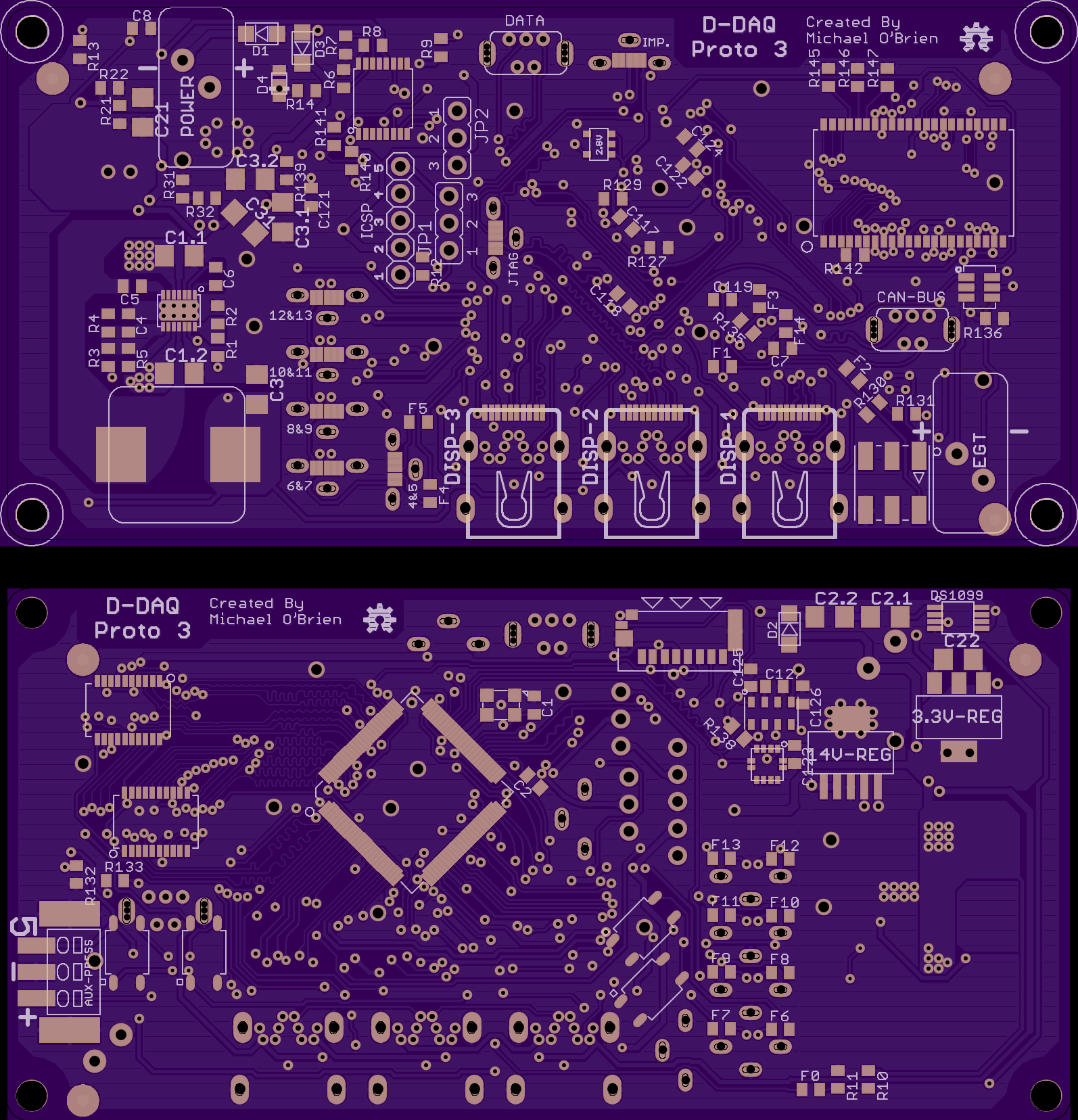
06/13/2014 at 13:57 • 0 commentsSo, as I'm about to pass out I've completed and uploaded the following PCBs:
- D-DAQ's Mainboard, Prototype 3 - The prototype number has been bumped to 3 because I've reworked the power supply subsystem and have added a 3.3V, 32.768 kHz charge pump to the 14V Rail. I've also lowered it's output voltage to ~13.7 V to allow it to behave a bit better in case there is any sag on the battery. The LDO has been replaced with a more thermally efficient version and though it also has more copper exposed, some of it is covered so it's performance characteristics are unknown. There are numerous footprint and silkscreen tweaks across the board. I'm testing a 603-SMD-footprint-on-a-diet too.
- Display Board - I've tweaked it a touch to allow what I have mentioned, jumpers to enable/disable the accent lights and warning lights separately. Fixed the text alignment too. I had to finish the adapter boards before ordering this one
- mDP Reversed Adapter - From a previous log last week I noted how the reversed adapter screwed over the pinout on the mainboard. This was fixed, but also required an adapter board. This one is for the Reversed receptacle.
- mDP Standard Adapter - This is an adapter for the standard pinout. This board and the other are required because a mDP cable doesn't have enough flex to make a 90˚ bend in side 2.25" dia. and also clear components.
The adapter boards use a 12-pin, right-angle header to perpendicularly plug into the Display Board. As long as a standard adapter is used with a mainboard that used a standard receptacle or reversed with reversed, you're good to go. This board also allows the Display Board's receiving pinout to stay constant and the terminations for the data lines and high(er) speed PWM line are on this adapter board.
For both of these little boards, I opted to try out freerouting.net to see how it's behave and if it'd be a bit useful. It allowed me to focus on other work while it hacked away at these guys. I did have to tweak a couple things on both after importing back into Eagle, but I'm happy with the work it did. I'm having it chug away at the mainboard to see if it can help out there at all. I'm fully aware though that it does no optimizations for maintaining contiguous ground planes so for some things it's use may be limited. I do want to see if it can remove several 10's of vias to reduce fabrication time and cost.
Anyhow, screen shot time:
![]()
![]()
![]()
![]()
Edit: Boards were ordered this morning and were scheduled to be panelized on Monday, however Osh Park panelized them and sent them in today. I'm far from being out of the tick of it. Right now, with those boards in the fab shop, and some modicum of confidence as to their functionality, I'm going to get started on the sensor board. Right now I have 10 planned and 3 test boards planned. Remember that the sensor boards have 2 inputs on them.
So far the boards that are planned are:
- 5V sensor to 3.3V - I'll be taking the op amp route.
- Dual EGT
- Dual Pressure - Using the same 100 PSI sensors most likely.
- Dual RTD tap - These will be interesting
- Pressure & EGT
- PWM to 3.3V - Not sure how I'll be doing them. an RC circuit is frequency specific. A small micro with a bit of code may be a better choice.
- RPM & Lift Needle - I'll be needing some fancy electronics for the latter
- RPM & Speed
- Pressure & RTD
- EGT & RTD
Overall this shouldn't be too "difficult" as once I have a circuit confirmed as solid and reliable, it's only a matter of getting in on a board next to another. If someone has any requests for different types of sensor inputs, I'm more than open to hear about them :)
-
Solution to 14V Rail Problem
06/12/2014 at 21:36 • 0 commentsNot a moment has gone by that I've been considering various solutions to the 14V rail problem. The previous plan was going to involved a simple charge pump to provide the input voltage to the 14V LDO. The current LDO being used has a max input voltage of 18V and a 3.3V clock will provide an easy output of +20V. After a week's deliberation, it comes down to 2 solutions: a SEPIC regulator or a charge pump and different LDO. There are pros and cons to both for what I'd be using the 14V rail for. First a little more in depth for why I'm going to so much trouble to have a 14V rail.
The display driver, the SEPS525, requires a 3.3V input for display logic and 14V input for display operation. The fun is the latter bit. The SEPS525 data sheets state a 8-18V input range with a absolute max of 19.5V. All 4 versions of the datasheet state this. However, every display datasheet using this driver state a 13.5-14.5V input range and an absolute max of 16V. Furthermore, the datasheets say that the the voltage range can be adjusted upon request. I'm presented with a chicken or the egg problem because I don't know which sheet I should go from. If I go with a lowest common denominator and pick a 12V input and it doesn't work, I have to come back to where I'm at now and start over.
Now, I am applying some LEDs for aesthetic treatment and pragmatism on the display boards. In order to pay homage to the community I'm developing this from, I'm using some LEDs with a forward voltage of 4.9V; they happen to be indigo color, which is the same as the cluster lights on the MK IV VW Jetta. I *could* drive them from the 5V rail, but I'm so close to the forward voltage, I can have other concerns so I need something higher and as such, I have a 14V rail already in the specs. This also eases things up a bit as I don't have to worry about sag when using high(er) current PWM driving of the LEDs and having my 5V or 3.3V supply lines ripple like crazy.
So, as such, I need to keep the 14V rail and it comes back to SEPIC or charge pump + LDO. Here is the short list of pros/cons for both.
SEPIC Pros:
- Very wide input range
- No voltage cut out limit for being slightly under or over the output voltage
- Excellent efficiency of 90% or better depending on use case
SEPIC Cons:
- 1 or 2 high(er) current inductors
- These are naturally large
- These are naturally expensive
- Part count of 12-15 components
- Controller IC requires solid fill for heat dissipation
CP + LDO Pros:
- Additional 4-6 components
- Effective brownout protection
- Standard sized components
- Higher power output per board space
CP + LDO Cons:
- Much less efficient
- Waste power = heat
- Upper input voltage range sensitivity.
Now, current output is a big concern for me. I will be having up to a 300 mA draw at 10% DC due to the PWM-driven LEDs. Even though it's at 10% DC, it's still a hunk of current and It's difficult to know if an LDO will survive the strain. They usually have internal current limiters from what I've read so even though I have a low average current draw, the instantaneous current draw might be a problem. I don't know though unless I build it. I don't have 3 additional weeks though to test a theory and then make a new version of the board if they theory is wrong. Even though on paper the SEPIC regulator seems a perfect fit, the size of the inductors and finding the right one to fit is difficult. Just the 7.3 uH inductor for the SMPS was a tough one to find and it's the smallest I could go with for it's series resistance and power rating.
I'm opting for the CP + LDO combo. I'll be using 4x2.2 uF MLCC caps arranged so 2 are in series for the clock's load and 2 are in parallel for the output load, a TL1963A LDO from TI, and a zener+ to ensure that I don't get more than 20 V to the LDO. Though the LDO is expensive, about $3 ea. vs ~$0.56 for the previous one, it's thermal resistance is realllllllly low for a SOT-223 package. The footprint is near identical to what I currently have and even beats out most Boost/Buck/SEPIC controller IC thermal resistances. Coincidently, the tab is connected to ground and on the backside of that board, I have a massive contiguous section of ground plane.
Due to the thermal performance, despite it's inefficiency, I can pull nearly 300 mA continuous out of this LDO at 50˚C ambient temperatures. It's a bit much for now, but given the option of larger displays which mean greater power draw in the future, this feels like a much more robust choice.
The charge pump to be driven by a SO-8 clock IC at 32.768 kHz with a 3.3V signal. With the equivalent of 1.1uF for the charge pump caps the voltage will vary greatly.However, at 10V input the charge pump bumps the voltage so its above the LDO's drop out for a 14.5V output. The lower capacitance reduces it's efficiency but in turn brings down the voltage to below the absolute max. Ironically, with the associated ripple from the reduced capacitance, the efficiency of the LDO is increased from ~67% to ~74% with 10uF caps under light load, and low 90s under 180 mA load. I was hopping for an input of 9V for the entire device, but right now that won't happen.
Side note: Thermal dissipation is a big deal for me. Though at regular temperatures, 20-30˚C, most of the components i have will easily function within the desired parameters, it will be common for this device to see 50˚C, or about 122˚F or higher in a car. Right now, I'm making sure the power subsystem(s) can handle 50˚C with no airflow. It may be able to operate beyond that, but I'm spec'ing this to only 50˚C operating temp for now. I've portioned a generous section of PCB copper to the LDOs and the SMPS so I should have a significantly lower thermal resistance than the max in the datasheets, and though I'm not going to run the math for irregular polygons just to find out how much better, some dirty math shows that I've double the amount of copper recommended in some cases.
-
14V Rail - Ahhhh, Nope!
06/07/2014 at 08:25 • 0 commentsSo I know of LDOs and why they're called such. For some reason I thought there was a bit of magic inside of them that allowed them to output a higher voltage. Maybe this was just me being stupid... Well anyhow, as I'm collecting part info and choosing the resistors and capacitors on mouser, I realized that hey, my LDO's drop out voltage won't allow me to produce 14V with an input of 14.4V. Oh, so that is why I've not ordered my 2nd prototype board yet ;).
Well, all is not lost on my existing board. It looks like I just have to cut a couple traces and jump the 5V output to the ground of the 14V regulator. I'll adjust the voltage divider circuit to output 9V and then I'll get my 14V output. Handy side effect is that I'll be able to still drive D-DAQ with a voltage down to ~9.5-10.5V which is at the low end of a car's voltage when cranking over.
While looking into a solution for this mistake, I came across a nice reference describing some details about LDOs. Though I've talked little about it, heat/thermal dissipation is a big worry of mine. In the current setup, the 5V LDO will be dissipating about 3.1W of power with a 14.4V input. Not a problem at all! :\
Well, thankfully with the current board layout, I have the 3.3V output of the SMPS running right next to the 5V LDO. In light of this new information, I'm switching the 3.3V SMPS over to a 5V output and then changing the 5V LDO to a 3.3V output. This will basically double the efficiency of that LDO (~35% to ~66%) and also drop its power dissipation to ~1W peak. The SMPS efficiency I estimate will be about the same, but maybe better; roughly 93-94%.
Finally, the 14V LDO. Not a problem except the LDO's dropout voltage is ~1.1V. I'm seriously kicking myself because I'm not sure what I missed here. Now, if I got rid of the LEDs, I could drop to a different LDO, but I'd have to use 2 of them in parallel in order to provide enough current for 3 displays when it's a hot day in a car that turns into an oven. This leaves me with an alternate issue: change the a different LDO or make the input voltage greater. I'm favoring the latter because sometimes there are problems outside of our control such as an alternator failure of similar electrical problems that creep up over the life of the vehicle. If the supply voltage drops below ~14.2V but stays above 6V, displays won't turn on, but every other bit will work just fine. Little bit of a problem if you're not familiar with the underlying hardware of D-DAQ when a dark display is indicative of a electrical problem of the car.
For these reasons, I'm going to attempt to bolster the 14V rail by doing 2 things. I'm going to switch over to either a pair of LDOs with a thermal dissipation of ~0.4W @ 50˚C at bare minimum or one that do double that with ease. Also, just before the LDO(s) though, I'm adding a single stage charge pump. I won't get doubled voltage, but I hope to achieve an operating voltage of at least 10V, possibly 9V.
Unfortunately these last two discoveries mean that the first prototype board of D-DAQ will not continue to get stuffed. Once these power supply subsystem changes are implemented on the schematic and board layout I'll again, let it sit for a day or two and have a look over it again and continue finding the components. Ironically, these issues were found as I'm simply going through and generating my BOM and double checking that everything looks sound.
-
Mini DisplayPort - The Headache
06/07/2014 at 02:43 • 0 commentsTwo days ago I noted that the mDP connectors are reversed, and I forgot to confirm their appropriate pinout before including them in on the project. I've already placed an order through a different supplier, ironically located near my place of work, for the correct orientation receptacles and today is when I set apart some time to figure out who named the right pinout. I knew this would be a bit of a headache, but hopefully not too much so. With the help of some "helping hands" I popped on two receptacles on the ends of the cable and switched my DMM to conductivity mode. Before I started mapping out the pinout, I looked back at the spec for DisplayPort to see what was supposed to happen inside the cable because I had read up on it being a cross over cable. I had 2 sources to reference: Wikipedia/Apple and displayport.net.
I mapped out both sources on a spreadsheet, used VLOOKUP to pull the names of signals so I didn't have to do this part by hand. My first reference is the footnote at the bottom of the pinout table on wikipedia stating:
This is the pinout for the source-side connector; the sink-side connector pinout will have lanes 0–3 reversed in order, i.e. lane 3 will be on pin 3 and 5 while lane 0 will be on pin 10 and 12.
My next reference, a little more detailed, was this graphic that I've seen dozens of times:
![]()
What the quote leaves out is what is shown in the graphic. The differential pairs are not treated as a single signal, but as individual conductors, thus the positive and negative lines are swapped. Next bit is the fact that the graphic is wrong. Pin 1 is defined as a ground in the spec. Wikipedia's first reference is Apple's 2008 DPF defining the specification, pin layout, and mechanical aspects of a cable and receptacle. Well, page 2 of that PDF has the proper pin layout, which corrects the above graphic when considering Mini DisplayPort. If you ever see if again there are 3 bits of info that are accurate: DP_PWR is a NC pin, i.e. the cable doesn't have a conductor for it, the AUX channels and Config channels do not change pins between source and sink.
Well, after mapping everything out and then flipping the pins, I came across 2 problems with using the reversed receptacle: the HDP line is connected to ground and the 14V line is connected to ground. I'll post later than the latter doesn't concern me with the Proto 1 board, but at the same time, it's a safety problem and also would make the board short out as soon as a cable is plugged into it. On the flip side, out of the 14 conductors available in the cable, I'm only using 12! I can simply reroute these 2 traces to the respectively unused pins and then I can use either of the receptacles in case there is a supply issue later down the road. Yes, it changes the pinout of the signals coming out of the other end, but at the same time, I'm using an adapter board to have the cable plug into the display board at a right angle. Just need 2 versions of that now ;).
-
Line Termination :(
06/05/2014 at 09:53 • 0 commentsOkay, this is a royal mess!!! I'm trying to make D-DAQ as robust as possible. Since I'm having 3 SPI signals go off-board, I know I need to terminate them. However, line termination is a royal pain to read about, especially when you're on a time crunch. I'll make this log short, too btw.
So, there are 4 basic types of terminations: Series/source, parallel, Thevenin, and AC. So, technically, it is possible for me to go back into the main board design, move traces around and series terminate each of my lines. However, if you've seen the board or it's graphical layout, it's hard to find space for 6 more resistors...
This leads to parallel termination which is basically a pull-up or a pull-down resistor at the end of the line. The issue here is that there is always current flow through the resistor whether it is sourced or sunk from the I/O pin. I'm dealing with a limited-to-no airflow environment and more power means more heat. Scratch that one.
When I read the word "best" I try to take note as to why the word is used. This was the case in the article on stack exchange for AC terminations. However, upon (PDF) further (website) reading (TI PDF) it's apparent that AC termination is tricky. Based on what I'm reading, I would not use this for long distance signaling and I'd have to set it up the capacitor for the frequency I'm operating at. D-DAQ is being designed to run the SPI bus at a specific speed but this doesn't mean that it will always be used at this speed. Capacitive reactance loading limits 1 of 2 things: bus speed, bus length. I can taylor the capacitor for a 20 MHz top end signal, but I'm limited to a 3 ft (4 ft really) cable. I'm sure someone will need a 6 footer at some point.
That leaves Thevenin. Basically it's a pull-up and a pull-down resistor pair. There is constant current, but due to the parallel nature of the resistors in line with the transmission line, the current draw is much less than parallel termination. As there is no capacitor in the circuit (ignoring transmission line capacitance), I don't have to worry about a limit to cable length or operating frequency.
If my understanding is accurate, I'll have an additional average current draw of ~9.2 mA per line on the 3.3V rail. For all 6 lines, that puts me at ~55 mA. Ironically, this is the current draw for 1 parallel termination.
-
Backend Refinements & Hangups
06/05/2014 at 01:34 • 0 commentsWhile parts are on order, might as well spend some time on the mainboard. Over the past week and a half, I've been tweaking trace placement to increase contiguous ground planes while removing vias, test fitting components and adjusting footprints, increasing the thermal relief sections of copper for the supply rails, and also fixing clearances.
Oh, and realizing that I forgot to put a pull-up on the MCLR pin, decouple it, and put a current limiter on it; important, huh? Speaking of semi-important things, the pin header footprints were revised for trace space and they were all shuffled so a jumper cannot be incidentally placed in a way that shorts a pin and so silkscreens can be read more easily.
I've removed more than a dozen vias for creating or jumping ground planes together but I've added half of them back to prevent any plane from behaving like an antenna. I noticed as well that clearances were 6 mil and though this meets many labs' capabilities, it doesn't make it cheap to manufacture. I've since adjusted everything sans 2 vias to 7 mil clearances, though I still have 6 mil traces in a number of areas. The 2 that fail are literally less than 1 mil off so I'm not fretting over it. I can increase trance widths to 7 mil, but will take more time than I'm willing to spend on it since it'd require reworking the MCU-SRAM section of the board.
The thermal relief areas for the 14V LDO, 5V LDO, and 3.3V SMPS were bolstered. When going over the LED power requirements, even with PWM, for the display boards, I saw that I was going to be cutting things close. The other issue I do not know if it'll be an issue is the EMI created by drawing 300-450 mA @ 14 V for about 10-30 us. All power traces were upped in size a bit too. I want a low of a temperature rise as is reasonable for the board.
Anyhow, I have added 3 fiducials on the board, both front and back, and they are on the top of the board and the bottom right. The top pair share the same Y-axis coordinate and the right pair share the same X-axis coordinate. Don't know if I'll ever pass it through a pick and place, but it didn't hurt adding them in. I happen to push the mounting holes close to the corners. Even if these are cutting off the corners, which they're not, they'll provide notches for mounting. Corners were rounded for "workability" as when this gets stuffed in a dashboard, wires are everywhere they'll help getting hung up.
Anyhow, I'm dubbing the current revision as prototype 2.3. I'll let it sit around for a few days and see if there is anything else that jumps out at me. Though the next week or so is dedicated to soldering and getting firmware loaded on the MCU, due to the oversight of the MCLR pin, I'm not sure how it'll behave. Thankfully, I can still place a PU resistor on the board, but it'll be a ways away from the MCU.
My last possible show stopper is the mDP port. It's a reversed, aka upside down, port so the odd and even pins are swapped. As this is a fundamental change to component that I did not realize, I need to verify that I'm not sending a signal down a ground/shield path and that I'm on the correct copper pairs so I know where to expect a signal to show. Once I have this sorted, I'll order up the latest prototype from a lab.
Proto 2.3 Front:
![]()
Proto 2.3 Back:
![]()
h, forgot to note, I've almost settled on an appropriate license for the board. Through the deliberation, it's apparent that if someone every will want to rip off the board, the license is irrelevant as that individual or group doesn't care about it. The license will only limit myself and those who want to use it while maintaining its integrity.