 SHAOS
SHAOSThis board is 1st one for NEDONAND project that was done in pcb-application from gEDA, because of its size (all previous board met free Eagle size limitations). This is 16-byte ROM for NEDONAND:
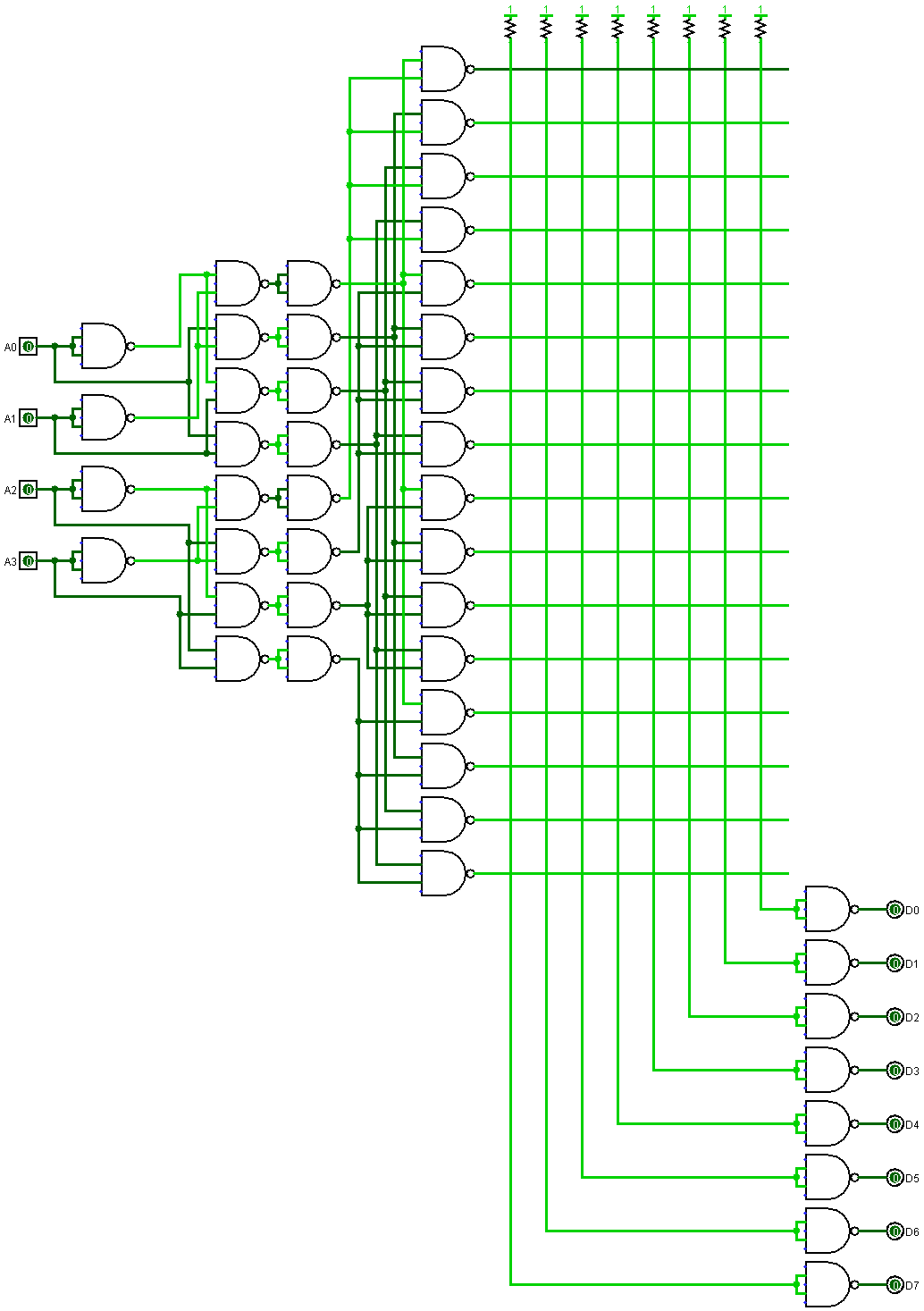
In every intersection above a diode could be put and it will drive that bit of those line down if this line is active (grounded) - so board should have 16 16-pin SIP sockets in order to make this ROM "re-programmable" manually:

4-bit address is going in through 4 header on the left and output is 12-pin header up with common memory interface that I will use for all memory boards for NEDONAND:
1) GND - ground
2) D0 - output bit 0
3) D1 - output bit 1
4) D2 - output bit 2
5) D3 - output bit 3
6) D4 - output bit 4
7) D5 - output bit 5
8) D6 - output bit 6
9) D7 - output bit 7
10) /RD (connected to LED in case of NEDONAND-16)
11) /CS (not connected in case of NEDONAND-16)
12) VCC - power +5V
Board had received from OSHPark and successfully tested - now it's also shared there...
Discussions
Become a Hackaday.io Member
Create an account to leave a comment. Already have an account? Log In.
I temporarily pull this board out of shared projects on OSHPark, because it has issues - some wires are going too close to pads and on the 1 board out of manufactured 3 it caused a short circuit to ground (output D6 was always "0") - so it has to be slightly redesigned...
Are you sure? yes | no