-
1Step 1
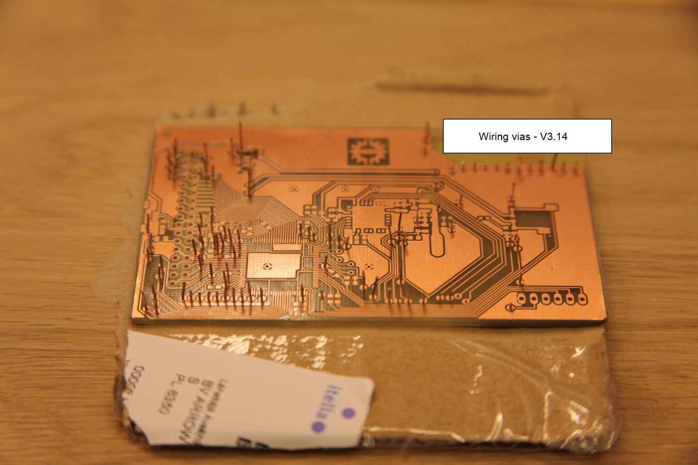
Building the KAPULA is quite straightforward. For the pcb, Bungard or similar 1.6 mm double sided, photoresist coated FR4 board is recommended. The 10 mil traces and spacings are thin enough to be spoiled by a stray speck of dust if self sprayed photoresist is used. In a laminar hood, maybe, but still... why? Changing the board material or thickness will detune the antenna, but in practice that is insignificant. The vias are gigantic to enable drilling with a wide variety of bits (we use 0.6 mm (24 mil)), the display connector holes should be drilled with 0.8 mm - 0.95 mm (31 mil - 37 mil) bits. The debug connector and microphone holes do not need to be drilled at all. Since most builders, including us, don't have access to through-hole-copper, almost all of the vias need to be fitted with copper wires soldered on both sides.
![Sticking the wires to the cardboard below]()
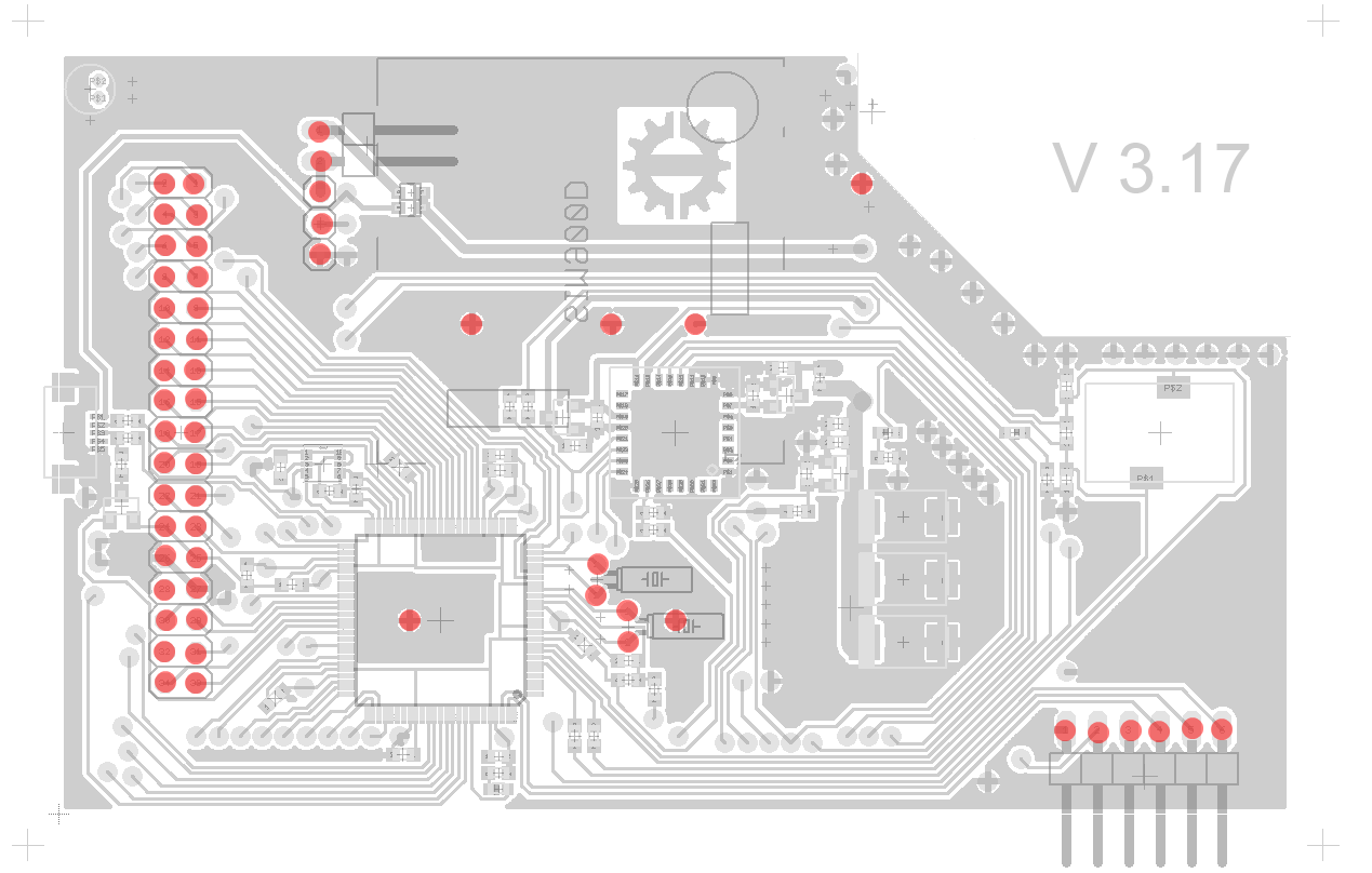
A few of the vias (like the one underneath the processor) are there only to let Eagle flood the copper to open areas. Do not wire the holes shown in red in the map below.
![]()
-
2Step 2
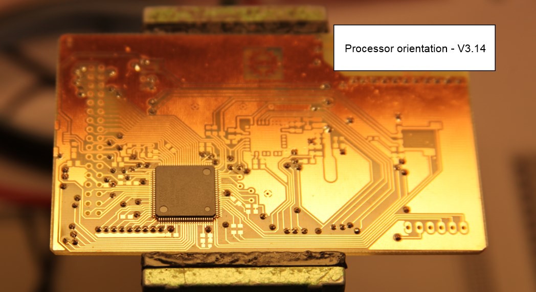
The components are most sensibly soldered starting from the processor and finishing with the Lepton. The functionality of the system can be tested without the Lepton and a mistake will be much less costly (... at least to the University. Did I mention the course is free for the students). For the processor the recommended method of soldering is drowning the pins in solder and then removing the surplus with a wick (see this excellent tutorial). This consistently results in better outcome than individually trying to solder the pins. Once more verify the orientation of the processor before soldering, as the LPC1768 has an unusual pin numbering and marking scheme... The crystal leads double as vias, so they should be soldered on both sides.
![]()
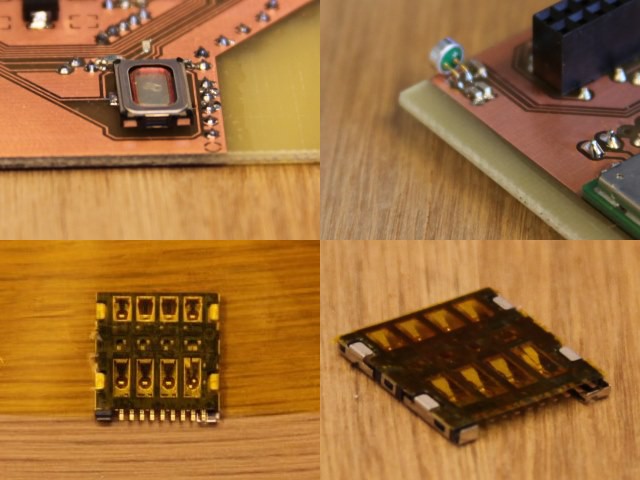
The bottom of the microSIM holder needs to be isolated from the ground plane underneath by a piece of Kapton tape. Position the tape exactly next to the pins, turn around and cut to size with a scalpel along the holder edges. Then clear the mechanical mounting pads on the sides, these are necessary to keep the SIM card in place. Given the proximity of the GSM antenna it was felt that a solid piece of copper is necessary there and later observations seemed to support that assumption.
![]()
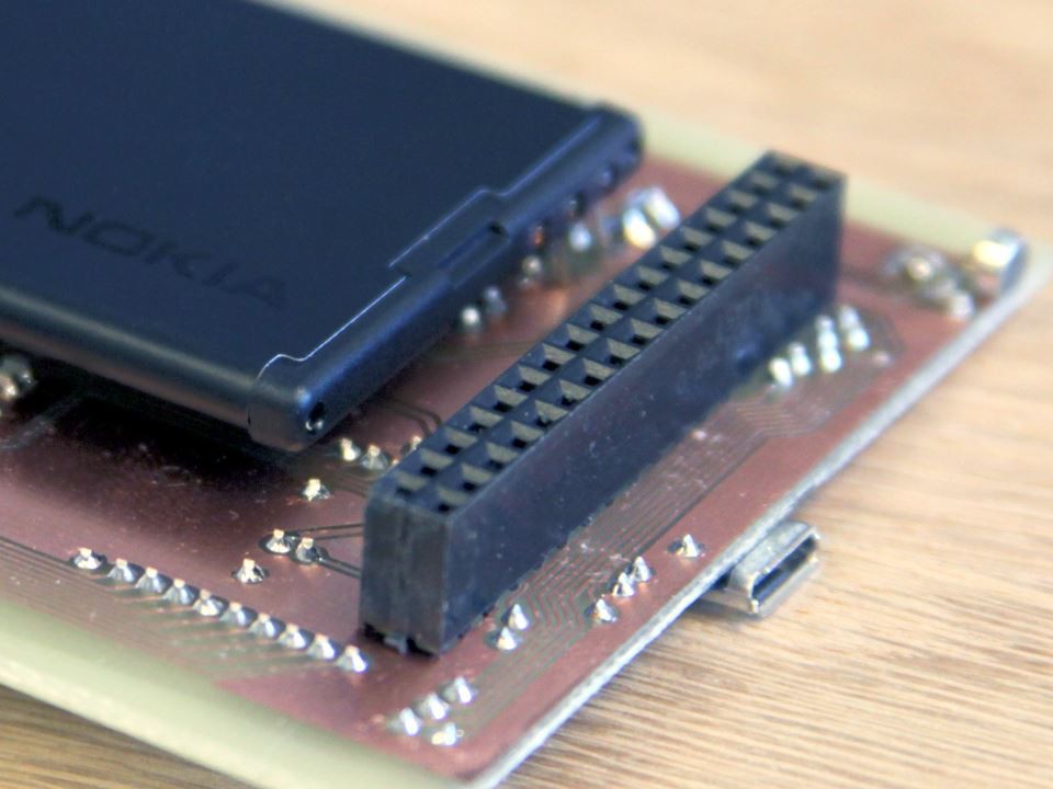
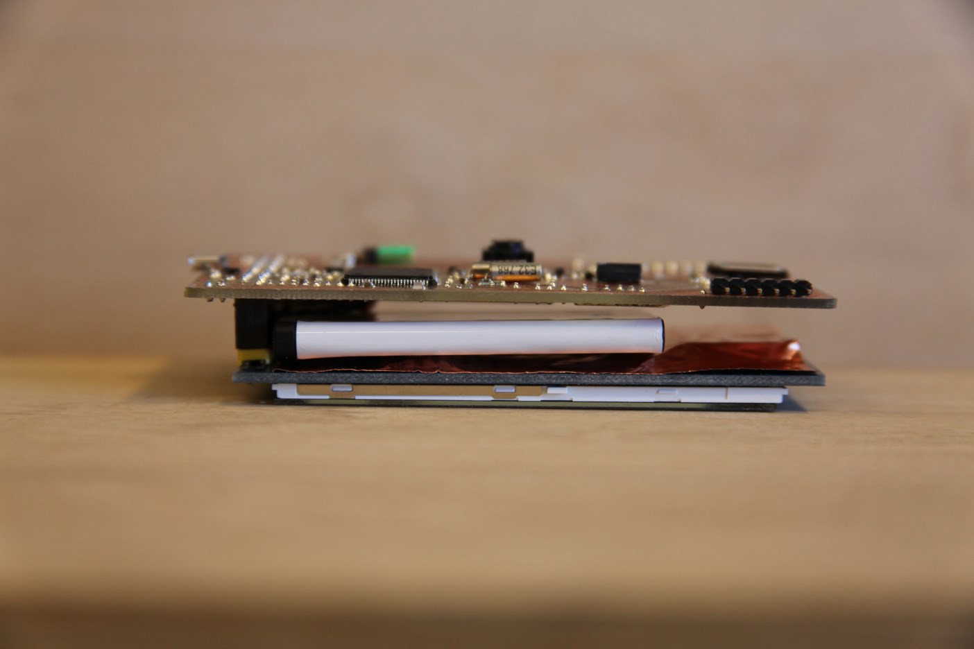
The display header can be either directly soldered to its place, or a female connector can be fitted in between. The latter results in a phone that is a couple of millimeters thicker (150 mils, maybe), but has superior tweakability. The phone battery is placed between the GSM module and the display and if there ever is a need to replace it, that is obviously impossible with the display in place (unless the battery has longer wires - also a valid option). The battery needs wires to be soldered to its terminals and this should be done with minimal heating. Fortunately most battery terminals are gold plated and instantly wet from the solder. All exposed battery pads, wires etc should be insulated with tape, epoxy or hot melt glue. Consider the battery a loaded gun when fitting the wires to the correct holes (battery pinouts vary) not letting them touch anything else. An optional piece of two-sided tape will secure the battery to the GSM module nicely.
![]()
![]()
![]()
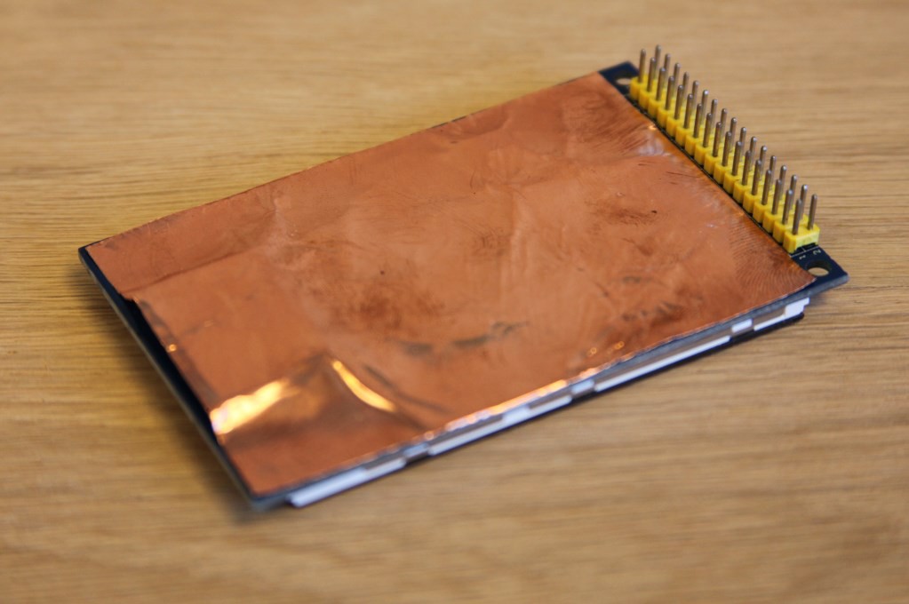
The display will benefit from additional shielding underneath with grounded copper tape (first plastic tape, of course) to reflect most of the antenna radiation. Otherwise some disturbances in the image can be seen. The SD card holder provides a perfect grounding point, being large and planar. Originally the antenna didn't have an attenuator circuit and the unshielded display occasionally crashed during the initial GSM burst! So did the processor without the filtering circuit on the reset line. The antenna seems simpler than it is, this design was a result of several iteration rounds and provides decent response even with nearby enclosure, hands and skull. The radiation pattern is not yet measured.
![]()
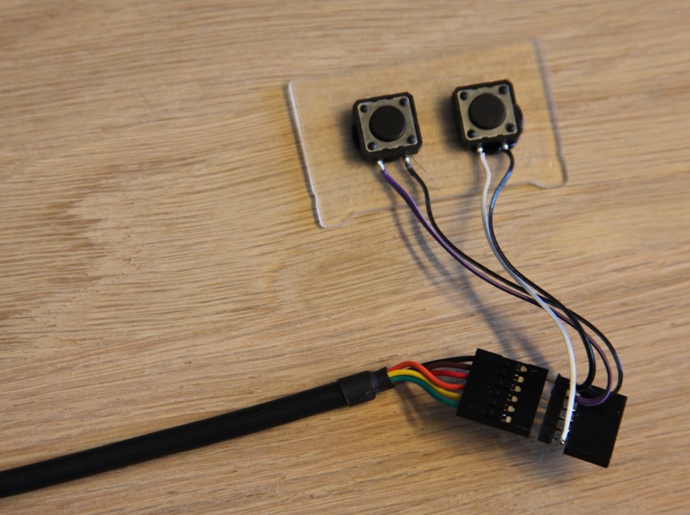
A pin header can be temporarily soldered to the debug connector. The pinout matches an FTDI cable with the exception of pins 2 (reset) and 6 (boot), which need pushbuttons to gnd (notice the two missing pins in the adapter). To reset the ARM the reset button is pressed, to flash it the boot button is pressed, the reset pressed, the reset released and the boot released. To actually download the new software, FlashMagic is used. The MBED .bin can be converted to the necessary .hex with the bin2hex64 utility in the files section. I cannot believe that google didn't find a bin2hex that would work both with files larger than 64 kB and in 64-bit Windows 7.
![]()
-
3Step 3
The GSM module needs a firmware update if MMS messaging is desired. The original firmware supports HTTP (and TCP in general), so sending pictures can easily be accomplished with it also, but not directly to other phones. The enhanced firmware supports MMS and HTTPS, although we have not tried the latter yet. All in all, the GSM communications seems to be a somewhat murky subject, with multiple cryptic ('bearer profile', say what now?) layers of functionality. The phone software contains a working solution for MMS, but that was a lot of (guess)work. At least it seems to be essential to close the API layers successfully and in correct order afterwards. Also, sending MMS messages seems to be insanely expensive compared to anything modern.
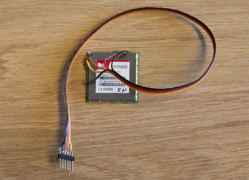
It is easier to update the module before it is soldered to the board. For that, one needs to solder wires to pins 1 (debug_rx), 2 (debug_tx), 12 (powerkey), 37 (gnd) and 38 (3.3 V). Contrary to the SIM900D documentation, it seems not to be possible to update the firmware through the main UART. Powerkey should be connected to gnd via a pushbutton (or improvise with a breadboard) and the rest to a standard 3.3 V FTDI cable in obvious order. In the image the header pinout complies with the debug adapter, the reset button connecting to the powerkey signal.
![]()
If the module is already on the pcb, wires can be connected to 1, 2 and any ground, connected to the FTDI cable and power provided by the phone battery. If the boot switch is pressed within one second after the reset is released, the software switches to GSM firmware update mode mirroring the state of the boot switch to the powerkey.
The firmware upgrading application and instructions, and the enhanced firmware are just a click away. That repository appears to depend on user uploads, so be sure to scan what you get.
KAPULA - The Thermal Smartphone
An open source, open hardware thermal camera smartphone project for freshman engineering students
 Karri Palovuori

Discussions
Become a Hackaday.io Member
Create an account to leave a comment. Already have an account? Log In.