 Blair Vidakovich
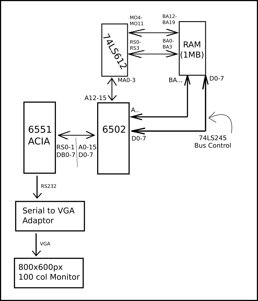
Here's my firs couple of hours making a simple conceptual flowchart for the architecture of the 8-Bit Portable Computer.
I don't have the protection circuitry for the 74LS612 MMU finished, so I didn't want to go into a complete electrical schematic.
The things missing in this diagram are:
- Memory-mapped ROM
- Memory-mapped IO
I anticipate that I may need a second 6522 ACIA in order to debug the system.
At the moment, most of the components for the computer are remaining very cheap, so I am hoping this may be able to be copied and built elsewhere.
Discussions
Become a Hackaday.io Member
Create an account to leave a comment. Already have an account? Log In.
It's a famous paged memory mapper! There is loads of information about it on 6502.org
See the datasheet here: http://pdf1.alldatasheet.com/datasheet-pdf/view/116938/TI/SN74LS612.html
And here are two different web pages giving information about it:
http://www.6502.org/users/andre/icapos/mmu65.html
http://www.6502.org/users/andre/hwinfo/ls610/index.html
Are you sure? yes | no
Thanks ! I have looked at Google and found some information.
I have never seen this chip in the wild...
Are you sure? yes | no
It looks similar to three 74ls189 where the address buses are multiplexed onto four address bits of the CPU and the 12 data bits are used to provide the higher address bits from A12 to A23?
Are you sure? yes | no
74LS612 ? Does that exist ? I have never seen that before........
Are you sure? yes | no
I think the ROM and the IO can be mapped in between the 74LS612 MMU and the RAM with some simple address logic circuitry
Are you sure? yes | no