-
New Thoughts On This Project
12/10/2021 at 23:06 • 0 commentsThe last couple of posts I made on this project were on the 2nd December. But, before then, I had not actually done any significant or substantial work on this project since some time in 2018--now almost 3 or 4 years ago.
I originally indicated, a few days ago, that I wanted to use a pre-existing hackaday.io project for the video output for this computer, but I have, yet again, changed my mind, and I think I need to post a longer project log in order to clarify and communicate my thoughts.
In this update, I want to:
- Inform you all that I am going to be using a pre-existing microcontroller platform (such as an Arduino, ESP32, or Raspberry Pi Pico, for example) instead of a 6502 for the project's CPU. Please see below for the rationale for this decision. In short, I believe using a microcontroller will greatly simplify, as well as cheapen the overall cost for others to construct this project independently.
- Bring you all up to date about the software stack I wish to use. I have since learned Common Lisp, and there is a happy co-incidence that the uLisp ('micro-Lisp') was brought to my attention. I will be using this software stack of Lisp for microcontrollers for this project.
- Clarify my thoughts about how to produce video output for this project. This has, aside from my meanderings about which kind of RAM design to use to support the 6502, been quite a sticking point for me for moving forward on actually constructing anything. In this post, I want to explore the options I have for producing a video display for this computer.
- Introduce you all to a new philosophical motivation I have for this computer. I have, since being away from hackaday, heard about 'solarpunk' and 'permacomputing'. I am now going to incorporate these two concepts into this project by (a) keeping this design as low in power consumption as is practicable; and (b) attempting to make the design for this computer as inexpensive and easily accessible to those with low incomes as possible.
- Specify, just briefly, what I imagine the human-interface aims/goals of this project to be. In other words, I want to inform you all that if this computer can (a) access gopher hypertext; (b) access IRC; and (c) perform some simple level of text editing, then I will consider this project 'complete'--and by that time, I can move onto developing more software for this computer design.
Radically Changing the Design
After refreshing myself with all my original development on this project, I have decided to radically change the design. I would be nice to use a 6502 CPU, with all of the supporting components and design of this project, but I think it is far too complex. I think there are far too many connections and components in order to make this a viable project for people to follow along and build their own version of this project.
uLisp, Lisp for Microcontrollers
I have spent quite a bit of time away from hackaday, but I have continued to be productive. I have been learning Common Lisp, as well as Emacs Lisp. Indeed I have been using Emacs as my window manager for a few years now, and do almost all of my work on my computer inside GNU Emacs.
My inquiries and investigations into Lisp brought this incredible project to my attention some time ago.
The project is called 'uLisp', and it implements some subset of Common Lisp for a wide array of embedded microcontroller computing platforms. I believe choosing a microcontroller supported by uLisp solves many problems at once, when it comes to constructing this project:
- It provides a complete software stack for the project. That is, uLisp allows a simple and coherent way for a human to take control of this computer's hardware, and extend its operation.
- It supports a wide variety of 8-bit to 64-bit microcontroller platforms, and therefore makes it as simple as selecting and acquiring, say, an Arduino in order to satisfy the requirements of this project that it be low in power consumption, powerful enough (and no more) to achieve the human-interface requirements, and follow the privacy and hardware safety requirements I originally set out for this project.
- It makes the project cheaper to construct by oneself.
- It makes the project trivially simple to construct by oneself.
Solarpunk and Permacomputing
I have been active on the fediverse in some capacity since 2017. Many people there are part of the 'solarpunk' and 'permacomputing' movements. This is already a very long a dense project update, so please see the following links for a quick FAQ for the rationale and justification for these philosophies:
- What is Solarpunk? (See the Solarpunk Manifesto)
- What is permacomputing? (See this webpage, and this 2021 update to it)
Video Output Woes
Blech. I have run out of time and energy, and cannot finish this log right now. I will finish up here quickly by saying that I still need to find a simple way to provide video out for this computer.
If you have any suggestions, I would be more than happy to explore what you have to contribute (:
~vidak
[to be continued]
-
Settling On Video
12/02/2021 at 05:09 • 0 commentsThis project seems to fit the bill quite well regarding video display:
https://hackaday.io/project/170499-vga-shield-wing
I think I will use this component for my computer's video (:
-
New Life.
12/02/2021 at 04:46 • 0 commentsIt has been many years since I have been here!
I am going to be breathing new life into this project (:
-
Using the Atari TIA (Television Interface Adaptor)
02/07/2019 at 11:48 • 0 commentsThis is just a quick blog post to say that I have revised my plan for this project a little.
I have decided to make the computer use 32K or 48K of RAM.
I have found a cheaper 4G cell breakout board than the one that I originally specified.
I have also decided not to go with the Hobbytronics open source serial-to-VGA video driver, and instead use the TIA from the Atari 2600 as the video chip for the computer.
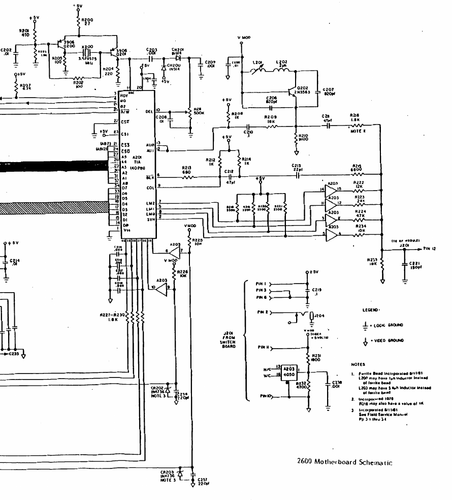
The following is the implementation of the TIA in the Atari 2600, which uses the TIA to generate a composite output, which is then combined into an RF signal.
And
![]() I will draw up schematics showing how I will change this circuit to display composite video and monoaural audio.
I will draw up schematics showing how I will change this circuit to display composite video and monoaural audio.
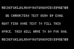
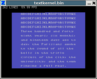
The TIA is a very versatile device which is capable of 128 colours in NTSC video, with one colour per scanline. With special coding, it is possible to draw up to 36 columns of text.
See THIS[1] forum post and THIS[2] blog post for more details.
This is an example of the text display. This is 36 columns. I think it is possible to go further.![]() And another example of text display on the TIA. This is 24 columns:
And another example of text display on the TIA. This is 24 columns:![]() Both the TIA and VIC chips are available for cheap online as new parts, and also in broken machines, so I think this is a good idea.
Both the TIA and VIC chips are available for cheap online as new parts, and also in broken machines, so I think this is a good idea.
I may experiment with the VIC from the VIC-20, to see which chip I like best.
The TIA is also capable of fantastic 8-bit graphics. -
Ideas for Handling Interrupts
04/12/2018 at 10:23 • 0 commentsCheck out this project's thoughts on handling interrupts: https://www.luke.maurits.id.au/projects/computers/lm512/
-
Another Previous 6502 Project!
04/12/2018 at 10:13 • 0 commentsJust discovered this projec here: (https://hackaday.io/project/18331-mkhbc-8-rx)!
-
Cellular Data
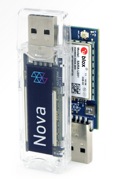
04/12/2018 at 07:47 • 0 commentsThis (https://hologram.io/nova/) website lead me to the ublox SARA modules.
I think I'll be using a celluar data module like this one (https://www.u-blox.com/en/product/sara-u2-series) in my design. I think it will necessitate another ACIA serial chip.
As far as I can tell, the ublox chips can interface via UART, and recieve AT commands. There are modules that do LTE and positioning as well.
![]()
-
Moving From the Exotic 74LS610 MMU to Normal Bank Switching
04/12/2018 at 05:12 • 4 commentsI have been trying to wrap my head around exactly how the 74LS610 Memory Management Chip will work in my Hackaday Prize competition entry. There is not a lot of complete documentation on exactly how to implement the 74LS610. So, ultimately, I decided to scrap using the chip, and I decided to use a simpler and more rough-and-ready solution to how to extend the memory of this internet-enabled 8 bit laptop I am building.
I did some searching, and I found a solution I can actually understand:
http://www.zcontrol.narod.ru/diagrams/ZramBankSwitch.pdf
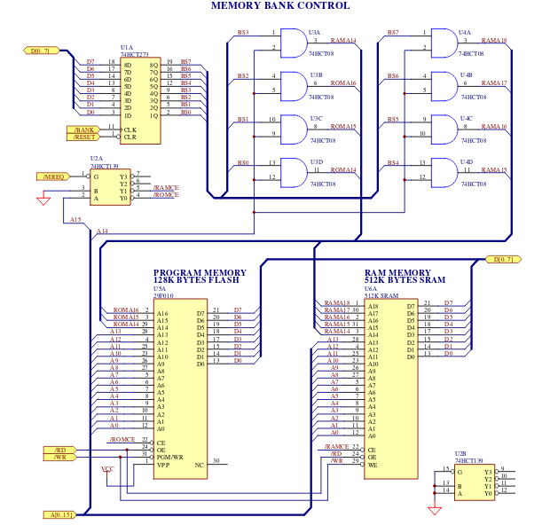
This document outlines how to extend the ROM of a computer to 128K bytes, and the RAM to 512K bytes. This is the schematic:
![]()
The incredible benefit of this solution is that it minimises the amount of programming needed in order to switch banks of ROM and RAM.
Selecting Between the ROM and RAM
The implementation uses one half of a 74HCT139 decoder to select between the ROM and RAM. When A15 is high, RAM is selected; when A15 is low, ROM is selected. A15 is gated with /MREQ to assure that the memory chips are enabled only when the bus access is for memory, and only when the address lines are stable.
The Bank Switch Latch
As the document outlines, a 74HCT273 eight-bit latch serves as the bank switch latch. Because this circuit is intended for a Z80 processor, the circuit requires the user to output bank switch information with a Z80 OUT instruction, which would generate the output strobe /BANK. Because we are using a 6502, I imagine we could do that with the VIA.
The document specifies that a 74HCT138 or similar part (not shown in this schematic) would interface with the Z80 processor to recieve an OUT opcode to generate the bank switch strobe and other needed I/O strobes. At power-on, the /RESET signal resets all the bank switches to zero.
The Eight AND Gates
The latched bank switch output signals, BS0 through BS7, are connected to one input of each of eight 74HCT08 AND gates. The outputs of these gates are used to generate extra address lines for the ROM and RAM chips—three for the ROM, and five for the RAM.
Using A14 to Gate the Bank Switching
Each of the eight 74HCT08 AND gates has its other input tied to Z80 address line A14. When A14 is high, the extra address lines will follow the values latched in the 74HCT273 bank switch latch. When A14 is low, the extra address lines will all be set low, regardless of the values latched in the bank switch latch. However the last values stored in the bank switch latch remain there, ready for the next access
to a bank-switched memory area.Very Simple!
As you can see, this is a very simple solution to what could be a complex problem. Using the VIA chip already being used in this design, and just by using A14 and A15 of the 6502, we are able to increase our total ROM addressable to 128K bytes, and RAM to 512K bytes. I think this will be sufficient.
The Memory Map
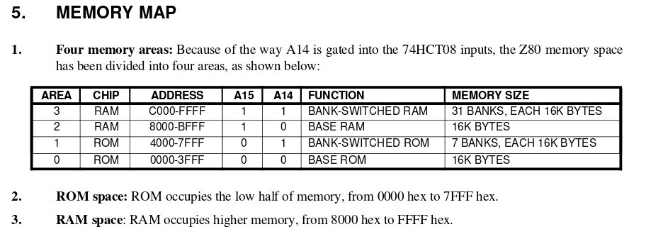
The document we are working with specifies this as the memory map of the design:
![]()
There are four areas in the memory map. The power of this design is that there are 16K bytes each of ROM and RAM which are base ROM and RAM. This means that these areas are not switched out upon switching banks, which means permament program information can be stored in these banks, which is very useful. I imagine we can section of parts of these 16K byte areas for IO. The stack can be located in the base RAM area, and the reset vectors needed for the 6502 can be located in the base ROM area.
A Bank Switch Shadow
There will need to be an area in the base RAM area which shadows the state of the bank switch latch. This is so the operating system of the computer can keep track of the state of the bank switch latch. This will be useful for multi-tasking applications.
-
Perhaps aim for 32KB or 48KB RAM.
04/10/2018 at 11:49 • 0 commentsI wanted to write quite a nice operating system for the new computer, so I thought about a megabyte of RAM would be useful, and make the task easier - but wrangling the MMU gives me some grief.
Perhaps it would be easier to just stick within the 2^16 memory space? Like 48KB or 32KB RAM.
I'll do some more research on virtual memory spaces for 16 bit memory spaces.
-
Second Effort at Constructing Architecture
04/08/2018 at 10:08 • 0 comments![]()
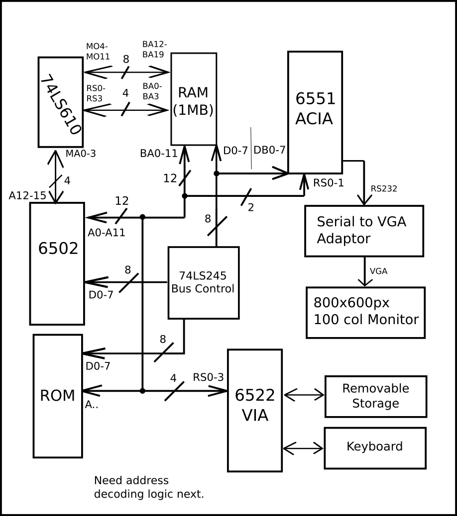
ROM and IO (through the 6522 VIA) is not that difficult.
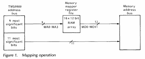
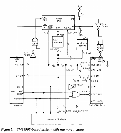
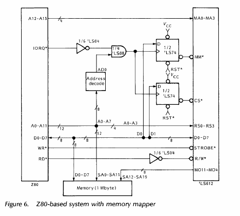
I need to find something to decode the address logic though - but that shouldn't be too difficult.I pirated this academic article - check out some of the diagrams from it. If you'd like a copy of the article I'd be more than happy to provide it.
![]()
![]()
![]()
8-Bit Portable Internet-Enabled Computer
A portable computer based on the MOS 6502 that aims to enhance security and privacy.
 Blair Vidakovich
 I will draw up schematics showing how I will change this circuit to display composite video and monoaural audio.
 And another example of text display on the TIA. This is 24 columns:
 Both the TIA and VIC chips are available for cheap online as new parts, and also in broken machines, so I think this is a good idea.