-
Hack Chat Transcript, Part 2
03/16/2022 at 20:13 • 0 comments![]() Thomas Parry did a livestream with me about his process
Thomas Parry did a livestream with me about his processhttps://www.zerotoasiccourse.com/post/livestream-with-thomas-parry/
![]() his day job is analog asic design, so he's good to see how a pro uses the open source tools
his day job is analog asic design, so he's good to see how a pro uses the open source tools![]() Matt, Thank you for sharing. As you know, chip design is not easy---or everyone would be doing it! :-)
Matt, Thank you for sharing. As you know, chip design is not easy---or everyone would be doing it! :-)![]() Any idea how many more shuttles are planned for the free open source stuff? I recall hearing 6 last year. Does #5 going in soon mean there will be only 1 more left?
Any idea how many more shuttles are planned for the free open source stuff? I recall hearing 6 last year. Does #5 going in soon mean there will be only 1 more left?![]() Hi Bruce, yes, it's not easy. Personally the long wait is a kller
Hi Bruce, yes, it's not easy. Personally the long wait is a kller![]() i remember improving so rapidly when the open source fpga tools came along and I could iterate on hardware a lot faster
i remember improving so rapidly when the open source fpga tools came along and I could iterate on hardware a lot faster![]() but mpw1 took a year so now I can learn from the mistakes I made then!
but mpw1 took a year so now I can learn from the mistakes I made then!![]() Hi Paul! at least another 4 this year
Hi Paul! at least another 4 this year![]() oh, that's good to hear. I still sometimes fantasize about having time for this....
oh, that's good to hear. I still sometimes fantasize about having time for this....![]() yeah!
yeah!![]() it does take quite a bit of time
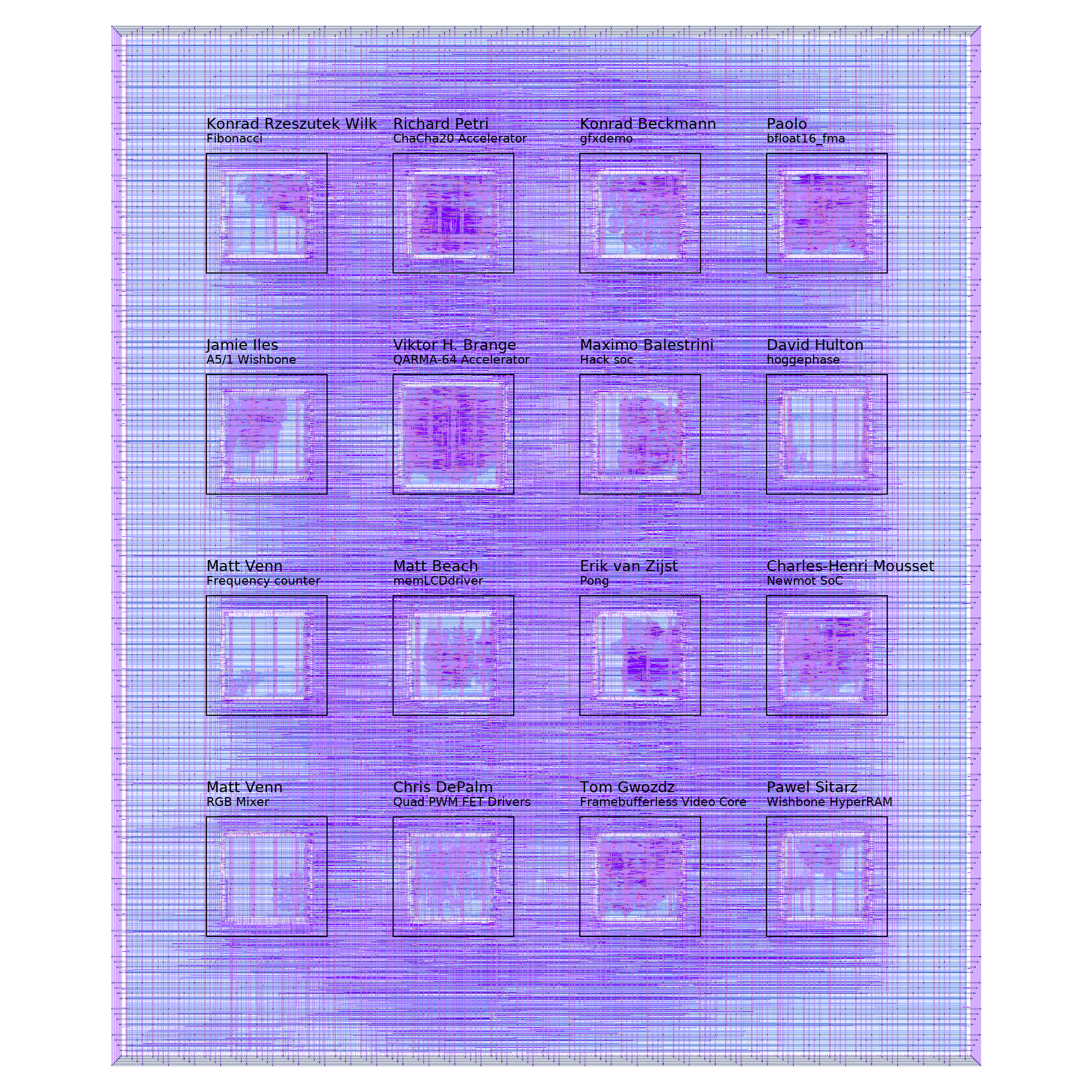
it does take quite a bit of time![]() does each die contain projects from multiple people + picorv32a?
does each die contain projects from multiple people + picorv32a?![]() Yup! I designed a chip 1993, which was made via Mosis. Spent all day and night on it for 3 months!
Yup! I designed a chip 1993, which was made via Mosis. Spent all day and night on it for 3 months!![]() wowza
wowza![]() Nick, my applications generally combine lots of designs from different people,
Nick, my applications generally combine lots of designs from different people,![]()
![]()
![]() Curious about logistics. Do they just deliver a naked die? If so, how do you put it to work? Or do they do wire bonding and a lead frame, etc?
Curious about logistics. Do they just deliver a naked die? If so, how do you put it to work? Or do they do wire bonding and a lead frame, etc?![]() but if you take a look at the submitted projects https://platform.efabless.com/projects/public you can see that most are just from a single person or group
but if you take a look at the submitted projects https://platform.efabless.com/projects/public you can see that most are just from a single person or group![]() nice one Paul! I still haven't got my name on a die yet!
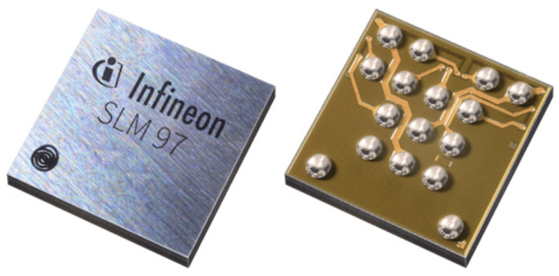
nice one Paul! I still haven't got my name on a die yet!![]() Dan, no they ship WLCSP at 0.5mm pitch
Dan, no they ship WLCSP at 0.5mm pitch![]() we got bare dies on mpw1 because they thought maybe it would help with the bringup
we got bare dies on mpw1 because they thought maybe it would help with the bringupif you don't know, we thought mpw1 was going to be a total write-off
![]() How did it get "fixed", can you describe what happened?
How did it get "fixed", can you describe what happened?![]()
https://www.zerotoasiccourse.com/post/mpw1-bringup/
MPW1 Bringup
I submitted my first ASIC designs to the free Google shuttle in December of 2020. In October 2021, we heard there were serious clock related problems with the management area of the chip due to issues with the toolchain. It seemed unlikely that anyone would be able to get anything beyond a single blinking LED from MPW1.
Read this on Zero to ASIC Course
![]() Was it only one fab run?
Was it only one fab run?![]() I do wish they'd do more maker friendly packages. Like QFN at least
I do wish they'd do more maker friendly packages. Like QFN at least![]() yeah, not sure why they don't. I heard a few answers, one was price and the other was performance
yeah, not sure why they don't. I heard a few answers, one was price and the other was performance![]() but tbh I didn't have too much problem with hot air
but tbh I didn't have too much problem with hot air![]() and I think probably that's not a big barrier if you've got to the point of receiving your own chips. Also in the future they'll be delivering a few assembled pcbs along with the rest of the ics
and I think probably that's not a big barrier if you've got to the point of receiving your own chips. Also in the future they'll be delivering a few assembled pcbs along with the rest of the ics![]() Tim, no we have had 4 now. 5th is on Monday
Tim, no we have had 4 now. 5th is on Monday![]() another 4 this year
another 4 this year![]() what package is used?
what package is used?![]() WLCSP
WLCSP![]()
https://www.zerotoasiccourse.com/terminology/wlcsp/
WLCSP
Wafer Level Chip Scale Packaging
Read this on Zero to ASIC Course
![]() pin pitch?
pin pitch?![]() 0.5 mm :)
0.5 mm :)![]() ouch
ouch![]() yeah, it was my finest up to that point
yeah, it was my finest up to that point![]() 0.8mm = everyday PCB fab, 0.5mm is more specialized
0.8mm = everyday PCB fab, 0.5mm is more specialized![]() we weren't expecting great yield due to the hold timing issues, but I got similar results to Sylvain tnt munaut
we weren't expecting great yield due to the hold timing issues, but I got similar results to Sylvain tnt munautso I think my soldering was ok
![]() just lots of flux and heat
just lots of flux and heat![]() fwiw, in my dream world of infinite hours in every day for open source, I really wanna try some analog stuff like 12/480 USB PHY and a 10/100 ethernet PHY....
fwiw, in my dream world of infinite hours in every day for open source, I really wanna try some analog stuff like 12/480 USB PHY and a 10/100 ethernet PHY....![]() Nick, I got pcbs from oshpark using their standard service and they looked good
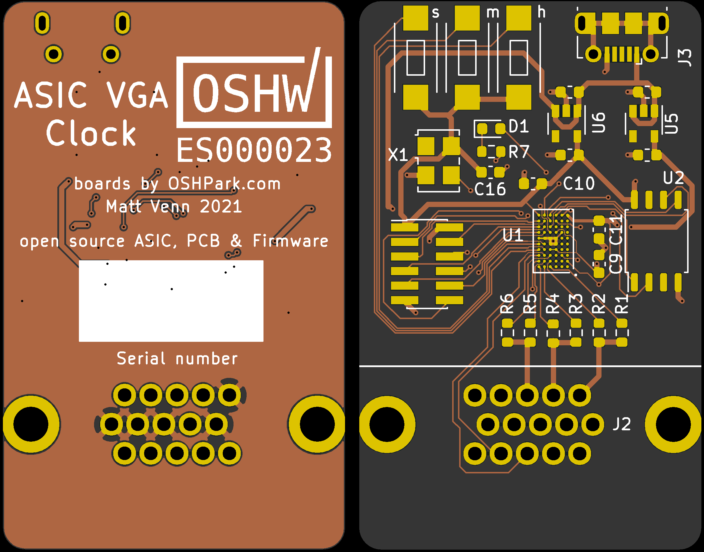
Nick, I got pcbs from oshpark using their standard service and they looked good![]() what via hole size + ring size? or were you able to do it without vias under the chip
what via hole size + ring size? or were you able to do it without vias under the chip![]()
https://www.zerotoasiccourse.com/post/vga_clock_pcb/
World's first certified open source hardware down to the chip level?
I'm very pleased to get OSHWA certification for my ASIC clock. Who knows, maybe this is a world first! The clock was submitted as part of MPW1. We're expecting silicon back in August/September, so it was time to get the PCB ready and try to source the other components!
Read this on Zero to ASIC Course
![]() the 4 centre balls are all ground, so you can put a via there
the 4 centre balls are all ground, so you can put a via there![]() so single via
so single via![]() but yeah, this would be expensive with pcbway
but yeah, this would be expensive with pcbway![]() oshpark let you break the rules, but I checked continuity of all the pads and looked good
oshpark let you break the rules, but I checked continuity of all the pads and looked good![]() are fuse bits possible on this process?
are fuse bits possible on this process?![]() We're up past the top of the hour now, so we'll have to let Matt get on with his evening. I just want to say thanks for a great chat -- I sort of followed it, seems like something you just have to dive into to really understand. Matt's course sounds like a great way to get going too. Thanks for the time, Matt! And thanks to everyone for the lively discussion and great questions.
We're up past the top of the hour now, so we'll have to let Matt get on with his evening. I just want to say thanks for a great chat -- I sort of followed it, seems like something you just have to dive into to really understand. Matt's course sounds like a great way to get going too. Thanks for the time, Matt! And thanks to everyone for the lively discussion and great questions.![]() Nick - I don't know about that
Nick - I don't know about that![]() @Nick Kelsey In the Sky130B PDK there is ReRAM. That can be used to make NV memory
@Nick Kelsey In the Sky130B PDK there is ReRAM. That can be used to make NV memory![]() Dan, thanks for the invite, and thanks everyone for the questions! Hope to see some of you tape out your first chips in 2022.
Dan, thanks for the invite, and thanks everyone for the questions! Hope to see some of you tape out your first chips in 2022.![]() Thanks a lot Matt, it was very helpful and I'll try to get into the course, seems an amazing thing to learn.
Thanks a lot Matt, it was very helpful and I'll try to get into the course, seems an amazing thing to learn.![]() Sounds awesome, appreciate and hope to do a project with your course!
Sounds awesome, appreciate and hope to do a project with your course!![]() thanks for chatting - I will sign up
thanks for chatting - I will sign up![]() join the mailing list for discount codes etc
join the mailing list for discount codes etc![]() Matt, Thanks again for sharing!
Matt, Thanks again for sharing!![]() like and subscribe lolz
like and subscribe lolz![]() Thanks @matt venn for the great chat
Thanks @matt venn for the great chat![]() Transcript coming up. Thanks everyone! Taking next week off, but we'll be back on the 30th to talk about thermal design issues for PCBs
Transcript coming up. Thanks everyone! Taking next week off, but we'll be back on the 30th to talk about thermal design issues for PCBs![]() have a great week everyone!
have a great week everyone!![]() Thanks, Matt!
Thanks, Matt! -
Hack Chat Transcript, Part 1
03/16/2022 at 20:12 • 0 comments![]()
![]()
![]() good day!
good day!![]() Hi Matt! Welcome aboard!
Hi Matt! Welcome aboard!![]() RPG map ?
RPG map ?![]() if you are 5nm tall, yes!
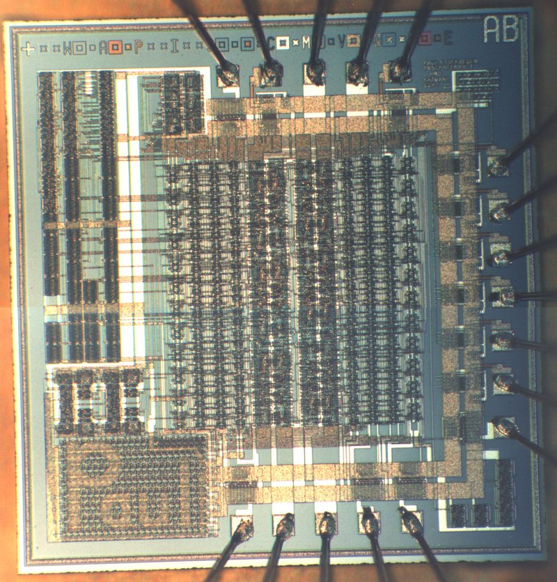
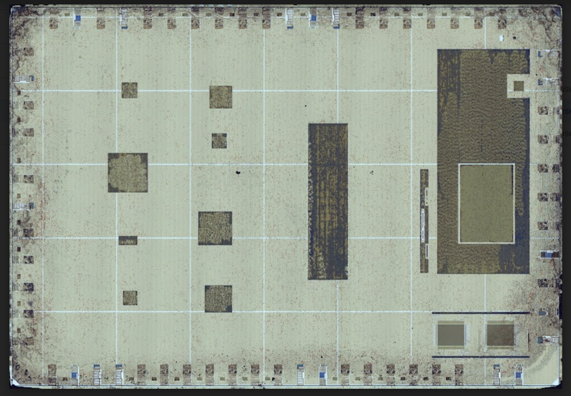
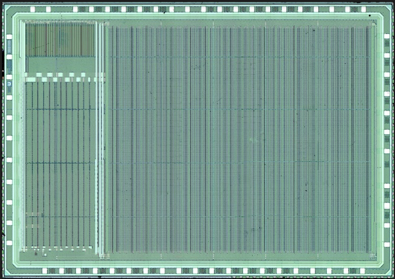
if you are 5nm tall, yes!![]() This looks like his MPW1 layout
This looks like his MPW1 layout![]() yup
yup![]() It's the new zombie map in Call of Duty
It's the new zombie map in Call of Duty![]() yeah it's got that ragged look
yeah it's got that ragged look![]() this is with top metal removed, which isn't a perfect process
this is with top metal removed, which isn't a perfect process![]() otherwise it looks like this
otherwise it looks like this![]()
![]()
![]() spreadsheet mode
spreadsheet mode![]() Welcome one and all, let's get started! I'm Dan, I'll be modding today with Dusan as we welcome Matt Venn to the Hack Chat to talk about open-source ASICs and spinning up your own silicon.
Welcome one and all, let's get started! I'm Dan, I'll be modding today with Dusan as we welcome Matt Venn to the Hack Chat to talk about open-source ASICs and spinning up your own silicon. Hi Matt! I know you've been around HaD quite a bit, but care to tell us a bit more about yourself?
![]() Funny that they look so different
Funny that they look so different![]() hi everyone
hi everyone![]() hi
hi![]() yes I've been doing electronics for a long time
yes I've been doing electronics for a long time![]() when I was a kid I bought maplin kits and assembled them, but didn't know how they worked
when I was a kid I bought maplin kits and assembled them, but didn't know how they workedI built a door lock that used some recycled 7 seg displays, and I hard wired them to spell 'open' when on, and nothing when off
![]() had no idea about how you would actually count numbers or change text!
had no idea about how you would actually count numbers or change text!![]() learnt slowly, got into microcontrollers, then fpgas
learnt slowly, got into microcontrollers, then fpgas![]() got involved with yosyshq and the formal verification tools
got involved with yosyshq and the formal verification tools![]() open source fpga toolchains
open source fpga toolchains![]() i was at week of open source hardware (WOSH)
i was at week of open source hardware (WOSH)when I saw Tim EDwards from Efabless showing a chip made with open source tools
![]() so I downloaded them and tried them on an fpga design (the vga clock)
so I downloaded them and tried them on an fpga design (the vga clock)![]() I looked at running a course so I could tape-out, but the cost was about 10k,
I looked at running a course so I could tape-out, but the cost was about 10k,![]() so I canned it. then 6 months later Tim Ansell announced the free shuttle program
so I canned it. then 6 months later Tim Ansell announced the free shuttle program![]() so I was in a good place and time to jump on and ride the wave
so I was in a good place and time to jump on and ride the wave![]() now I have 4 tapeouts and preparing for my 5th
now I have 4 tapeouts and preparing for my 5th![]() 160 people have taken my course and about 40 have taped out
160 people have taken my course and about 40 have taped out![]() mpw5 tapes out on Monday, so I'm getting things ready for that at the moment
mpw5 tapes out on Monday, so I'm getting things ready for that at the moment![]() what is the process size?
what is the process size?![]() 130nm, which is a kind of hybrid I think. The gate width of the standard cell library are 150nm
130nm, which is a kind of hybrid I think. The gate width of the standard cell library are 150nm![]() that would be ~1.2V?
that would be ~1.2V?![]()
![]()
![]() 1.8v core
1.8v core![]() Can you talk about what sort of FPGA designs can be easily ported? And what's harder coming from an FPGA?
Can you talk about what sort of FPGA designs can be easily ported? And what's harder coming from an FPGA?![]() the easiest is pure digital with no hard ip blocks like multiplies or brams
the easiest is pure digital with no hard ip blocks like multiplies or brams![]() you can synthesise small memories with yosys out of flip flops but they are big and don't scale well
you can synthesise small memories with yosys out of flip flops but they are big and don't scale wellwe have openram for some hard sram blocks, 1kb in size
![]() And what if we wanted to multiply - just let it synthesize it?
And what if we wanted to multiply - just let it synthesize it?![]() you could easly build a multiplier as well, for a dsp block but it would probably be quite big and not as efficient as one you'd get on an ecp5 for example
you could easly build a multiplier as well, for a dsp block but it would probably be quite big and not as efficient as one you'd get on an ecp5 for example![]() yeah
yeah![]() try not to divide!
try not to divide!![]() Right, that's true on FPGAs too
Right, that's true on FPGAs too![]() Can you give an idea of what sort of timing / frequency can be had?
Can you give an idea of what sort of timing / frequency can be had?![]() The MPW has 16 slots of 300x300 um areas. Have any of the 160 been too constrained by this for their circuit design?
The MPW has 16 slots of 300x300 um areas. Have any of the 160 been too constrained by this for their circuit design?![]() so you can do ghz no probs
so you can do ghz no probs![]() but we have limited bw on the ios, they are quite old and only really go up to 50mhz
but we have limited bw on the ios, they are quite old and only really go up to 50mhz![]() 300um x 300um or 800um x 800um max size - roughly how many pads and how many gates is realistic?
300um x 300um or 800um x 800um max size - roughly how many pads and how many gates is realistic?![]() there is an 'analog' version of the submission process that gives you 11 pads with no io pad, so you would have to deal with drive current, esd protection etc yourself, but then you could get ghz in and out of the chip. and it's wlcsp so quite good for high frequency
there is an 'analog' version of the submission process that gives you 11 pads with no io pad, so you would have to deal with drive current, esd protection etc yourself, but then you could get ghz in and out of the chip. and it's wlcsp so quite good for high frequency![]() How does that work if you only have 50 MHz in - are there PLLs you can design in?
How does that work if you only have 50 MHz in - are there PLLs you can design in?![]() James, that's actually just what I do for my group submissions
James, that's actually just what I do for my group submissions![]() so it's a sort of IP/block for the IOs and the design of that is what limits the I/O frequency off the chip?
so it's a sort of IP/block for the IOs and the design of that is what limits the I/O frequency off the chip?![]()
https://www.zerotoasiccourse.com/post/mpw2-submitted/
MPW2 Submitted
We did it! 14 people from the course got their designs into the group submission, and the project was accepted for fabrication. Silicon here we come! You can get all the details on all the projects from the Efabless submission And see how I put the application together here.
Read this on Zero to ASIC Course
![]() the full area is 3000 x 3600 um
the full area is 3000 x 3600 um![]() there are 40 slots on the free shuttle
there are 40 slots on the free shuttle![]() I started off applying for 1 each on mpw1 and 2 but from 3 onwards I am putting more on
I started off applying for 1 each on mpw1 and 2 but from 3 onwards I am putting more on![]() What can you tell us about that frequency counter on there?
What can you tell us about that frequency counter on there?![]() Ian, yes it's old io inheritted from cypress
Ian, yes it's old io inheritted from cypress![]() Tom, it's a very simple design I made to teach basic digital design to people who haven't touched digital design before
Tom, it's a very simple design I made to teach basic digital design to people who haven't touched digital design before![]() edge detecter, counter, 7 seg driver
edge detecter, counter, 7 seg driver![]() Are each of the designs driven by the PicoRV32 core or are they attached directly to package I/O?
Are each of the designs driven by the PicoRV32 core or are they attached directly to package I/O?![]() Do you know how things are looking on the analog side for these shuttles now? I started looking at the very start and it was very rough with untrustworthy models. Has this improved?
Do you know how things are looking on the analog side for these shuttles now? I started looking at the very start and it was very rough with untrustworthy models. Has this improved?![]()
https://github.com/mattvenn/frequency_counter
GitHub - mattvenn/frequency_counter
You can't perform that action at this time. You signed in with another tab or window. You signed out in another tab or window. Reload to refresh your session. Reload to refresh your session.
![]() If you only have 50 MHz in - are there PLLs you can design in?
If you only have 50 MHz in - are there PLLs you can design in?![]() the picorv32 is a coprocessor. it loads the gpio configuratoin and then you can ignore it. but you could add some wishbone peripheral for example and use it to accelerate the pico
the picorv32 is a coprocessor. it loads the gpio configuratoin and then you can ignore it. but you could add some wishbone peripheral for example and use it to accelerate the pico![]() I usually attach my designs to the output/input pins
I usually attach my designs to the output/input pins![]() I'm not familiar with wishbone peripherals
I'm not familiar with wishbone peripherals![]() and to handle multiple designs; on mpw1 I used a big mux (the big rectangle in the first pic I posted), and for mpw2 onwards used tristate outputs
and to handle multiple designs; on mpw1 I used a big mux (the big rectangle in the first pic I posted), and for mpw2 onwards used tristate outputs![]() itls like 32bit wide spi
itls like 32bit wide spi![]() Bruce, we have a DLL that can do up to 270 mhz
Bruce, we have a DLL that can do up to 270 mhz![]() Impressive!
Impressive!![]() Patrick, analog is getting better. 2 people to watch are Harald Pretl from JKU and Thomas Parry
Patrick, analog is getting better. 2 people to watch are Harald Pretl from JKU and Thomas Parry![]() wishbone is an open bus standard used for open FPGA IP and apparently in ASICs by now
wishbone is an open bus standard used for open FPGA IP and apparently in ASICs by now![]() Harald is taping out an audio DAC on MPW5 and Thomas is working on 5ghz satellite transceivers
Harald is taping out an audio DAC on MPW5 and Thomas is working on 5ghz satellite transceivers![]() you can get to the specs for wishbone from here: https://en.wikipedia.org/wiki/Wishbone_(computer_bus)
you can get to the specs for wishbone from here: https://en.wikipedia.org/wiki/Wishbone_(computer_bus)![]() If anyone else is lost in the jargon, you can get an explanation here:
If anyone else is lost in the jargon, you can get an explanation here:![]()
https://www.zerotoasiccourse.com/terminology/
Terminology
Learn how to make your own chips!
Read this on Zero to ASIC Course
![]() Thanks for the update @matt venn
Thanks for the update @matt venn![]() Thanks @Dan Maloney
Thanks @Dan Maloney![]() I was going to post a link to the projects on efabless website but they have just updated the website and the old links are 404
I was going to post a link to the projects on efabless website but they have just updated the website and the old links are 404![]() So, just to clarify, the class is not about making chips, but about making ASICs. How does one know what should go on an ASIC and what on a processor? Let's say for example, a sata controller to use with a riscv chip?
So, just to clarify, the class is not about making chips, but about making ASICs. How does one know what should go on an ASIC and what on a processor? Let's say for example, a sata controller to use with a riscv chip?![]() @Nick Kelsey To get an idea of what density is achievable yosys compiles the picorv32a riscv core to ~15K cells in ~150000um^2, so roughly 400um on a side.
@Nick Kelsey To get an idea of what density is achievable yosys compiles the picorv32a riscv core to ~15K cells in ~150000um^2, so roughly 400um on a side.![]() Alvaro, I suppose I don't see much difference between an ASIC or an IC. maybe volume? same process in design and manufacture
Alvaro, I suppose I don't see much difference between an ASIC or an IC. maybe volume? same process in design and manufacture![]() Eric, got any comments on that?
Eric, got any comments on that?![]() when you say processor, I think CPU, something that goes in your phone or laptop
when you say processor, I think CPU, something that goes in your phone or laptop![]() that's very general purpose, jack of all trades, master of none
that's very general purpose, jack of all trades, master of none![]() if you need to accelerate some application, like the sata controller, then you'd design a custom chip for doing that
if you need to accelerate some application, like the sata controller, then you'd design a custom chip for doing that![]() but you could also use the same tools and process to design a general purpose cpu
but you could also use the same tools and process to design a general purpose cpu![]() does that help?
does that help?![]() Yes, thanks. So if I wanted to build a sata chip or a riscv, the course would be a nice help to learn how to do it.
Yes, thanks. So if I wanted to build a sata chip or a riscv, the course would be a nice help to learn how to do it.![]() Matt, As I recall, back in the early 1990s, it cost a minimum of ~$100K to make an moderately complex ASIC using a fab like VLSI. How has that cost changed today?
Matt, As I recall, back in the early 1990s, it cost a minimum of ~$100K to make an moderately complex ASIC using a fab like VLSI. How has that cost changed today?![]() Can you talk a little bit about the design tools used for fabrication? With FPGAs there are very simple things to use like ICEStudio where you just draw the fpga design. How easy are the tools to build an ASICs?
Can you talk a little bit about the design tools used for fabrication? With FPGAs there are very simple things to use like ICEStudio where you just draw the fpga design. How easy are the tools to build an ASICs?![]() Alvaro, yes. I should have said in my intro, that I love science communication as much as I love actually messing around with electronics and hardware design. Now that the barrier to entry is so much lower for this field, I wanted to help people into it. So I am now basically split half science communciation with the course and half engineering with learning how to make chips and get them working.
Alvaro, yes. I should have said in my intro, that I love science communication as much as I love actually messing around with electronics and hardware design. Now that the barrier to entry is so much lower for this field, I wanted to help people into it. So I am now basically split half science communciation with the course and half engineering with learning how to make chips and get them working.![]() Bruce, I'm not sure how that cost breaks down. But the traditional industry standard (cutting edge) tooling is 100k per seat per year
Bruce, I'm not sure how that cost breaks down. But the traditional industry standard (cutting edge) tooling is 100k per seat per year![]() the open source tools are no where near the PPA (power performance area) which are common metrics
the open source tools are no where near the PPA (power performance area) which are common metrics![]() but the actual cost of getting 100 chips made is about 5 to 10k $
but the actual cost of getting 100 chips made is about 5 to 10k $![]() Joining late, but wanted to throw out that Parallax's P1 has been available for quite some time here https://www.parallax.com/propeller-1/open-source/
Joining late, but wanted to throw out that Parallax's P1 has been available for quite some time here https://www.parallax.com/propeller-1/open-source/![]() sky130 is about 20 years old, and the mask costs are about 200k $, then maybe 1k per wafer with 4000 chips on t
sky130 is about 20 years old, and the mask costs are about 200k $, then maybe 1k per wafer with 4000 chips on t![]() so people join together to do an MPW (multi project wafer) run, and split the high NRE cost of the masks between 40 people
so people join together to do an MPW (multi project wafer) run, and split the high NRE cost of the masks between 40 people![]() how about other interesting cells beyond gates for this process, for example fuse bits, eeprom cells, analog cells, etc
how about other interesting cells beyond gates for this process, for example fuse bits, eeprom cells, analog cells, etc![]() Matt, back in the 1990s the design tools were always more expensive than cost for prototyping chips! Hasn't changed it seems!
Matt, back in the 1990s the design tools were always more expensive than cost for prototyping chips! Hasn't changed it seems!![]() Nick, I don't know too much beyond the digital side of things. We have pcells (parametric cells) for analog
Nick, I don't know too much beyond the digital side of things. We have pcells (parametric cells) for analog![]() so you can size your own transistors, but the analog flow is very manual and hands on compared to the digital flow
so you can size your own transistors, but the analog flow is very manual and hands on compared to the digital flow![]() sky130b is a variant of sky130a and with a slightly different layer stackup we can have re-ram (resistive ram), but I know nothiing about it
sky130b is a variant of sky130a and with a slightly different layer stackup we can have re-ram (resistive ram), but I know nothiing about it![]() interesting
interesting![]() guessing analog is more like laying out a PCB vs digital which is verilog to a layout compiler?
guessing analog is more like laying out a PCB vs digital which is verilog to a layout compiler?![]() Nick, yeah and you have to size all the transistors yourself and make sure your design simulates to achieve your requirements
Nick, yeah and you have to size all the transistors yourself and make sure your design simulates to achieve your requirements![]() Thomas Parry did a livestream with me about his process
Thomas Parry did a livestream with me about his processAbout Us Contact Hackaday.io Give Feedback Terms of Use Privacy Policy Hackaday API
 Lutetium


