 danjovic
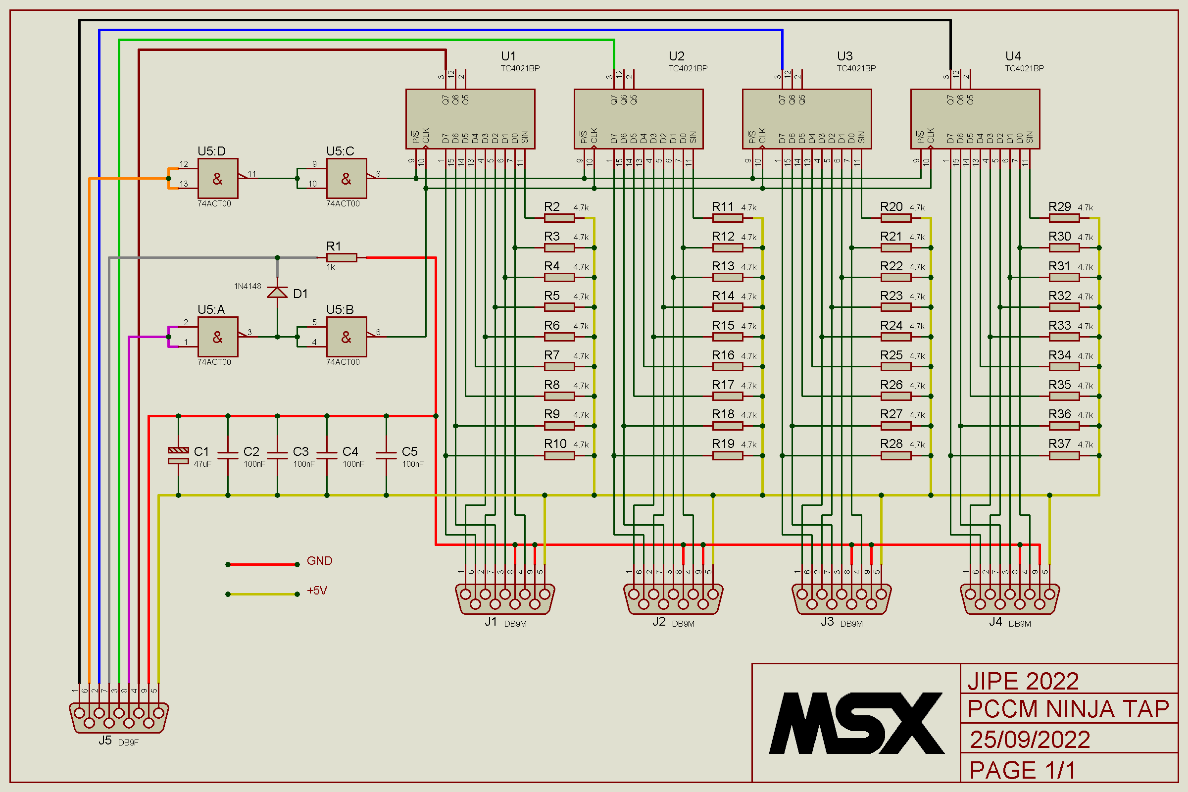
User Jipe from MRC (and MSX Village) reverse engineered its Ninja Tap adapter to obtain the schematics
https://msxvillage.fr/upload/pccm_ninja_tap.png
Luckly I was on the right track, being the most relevant difference the SI inputs of the 4021 being pulled up instead of down.
The original circuit uses a 74ACT00 chip not only to feedback the inverted state of signal of pin 8 (pulse) but also to drive the 4021 CLK and LATCH signals (maybe this was the main purpose of the '00 chip).
I have found another error on my circuit. but it was due to lack of attention. Pins 6 and 7 on the input ports were inverted, as D7 on the 4021s shall read the signal of Trigger A and D6 should read Trigger B, not the opposite.
The redrawn schematics is show below:

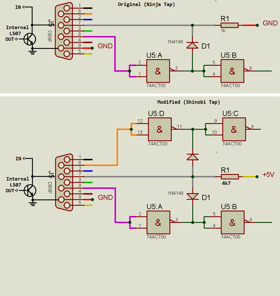
I have also updated the schematics for the Shinobi Tap, but changed the design of the feedback circuitry to avoid contention, and added a second feedback to allow differentiation between Ninja Tap and Shinobi Tap.
Detection can be performed using the expected states. First set pin 7 to High to release the open collector output at this pin.
| Pin 6 (Write) | Pin 8 (Write) | Pin 7 Read, no Tap | Pin 7 Read,Ninja Tap | Pin 7 Read,Shinobi Tap |
|---|---|---|---|---|
| LOW | LOW | HIGH | HIGH | HIGH |
| LOW | HIGH | HIGH | LOW | LOW |
| HIGH | LOW | HIGH | HIGH | LOW |
| HIGH | HIGH | HIGH | LOW | LOW |
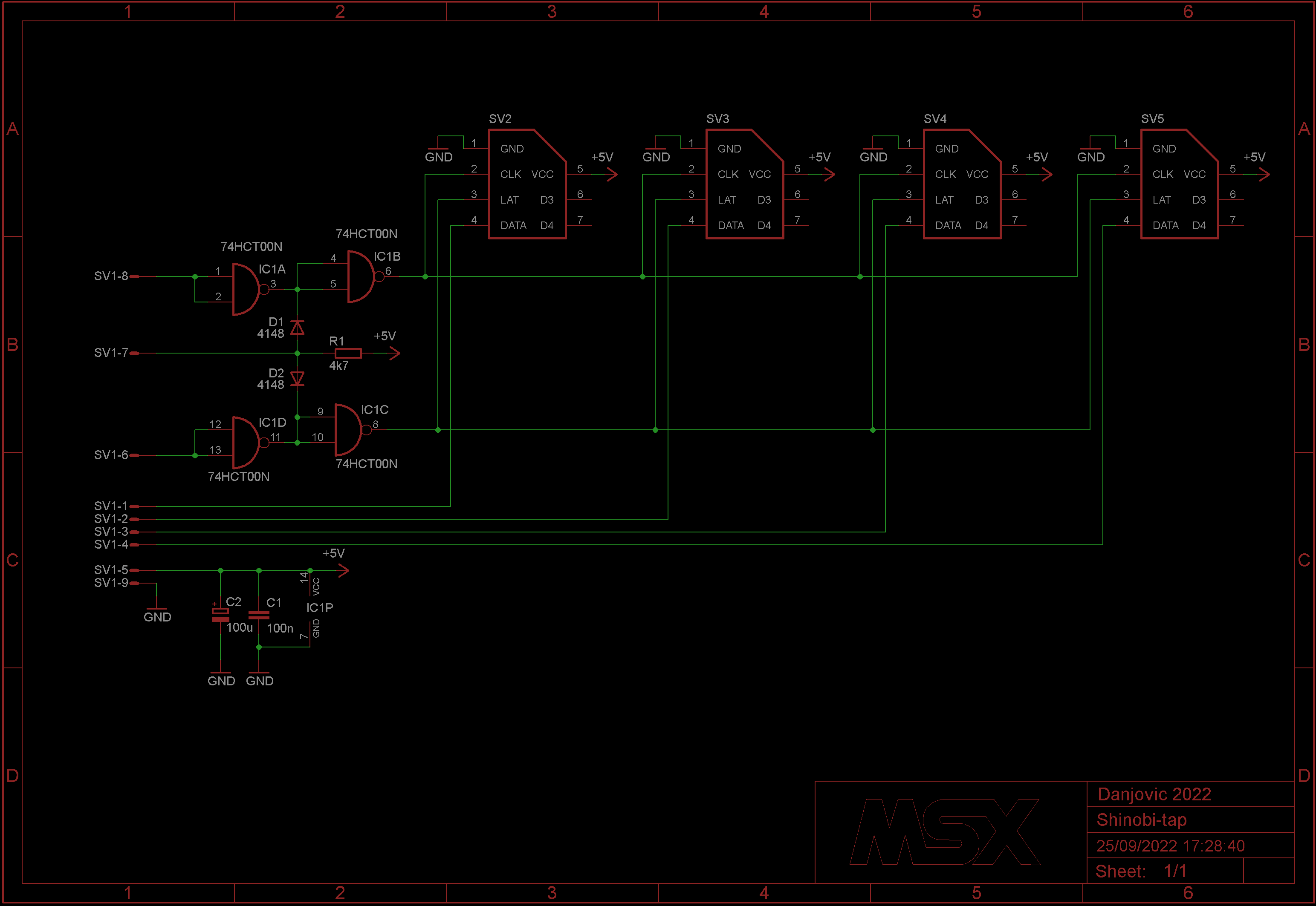
New Shinobi Tap circuit:
Discussions
Become a Hackaday.io Member
Create an account to leave a comment. Already have an account? Log In.