 Sergey Novikov
The article discusses the process of creating a program for initializing and controlling the ad9363 chip. The described approach is applicable for the entire ad936x family. Everything is implemented under the clone of ADALM-Pluto using Vivado 2021 and Vitis 2021 in C.
I am not an expert in ad9361 programming. This is an area that I want to explore. I’m trying to figure out the basics and it’s easier for me to learn when I see how it works. That’s why I’m doing this. Not because I already know everything about the ad9361. And if you also learn something from reading my article, that would be great. But please don’t rely on my articles to understand the theory. There are many excellent books and other sources on this topic where you can find more information. I hope that through this article you will learn how to apply some of the basic principles of ad936x programming in real systems. If you notice a bug or something that can be improved, please write to me in the comments or private messages. Then we can study together, and maybe I can fix it and show it in new articles.
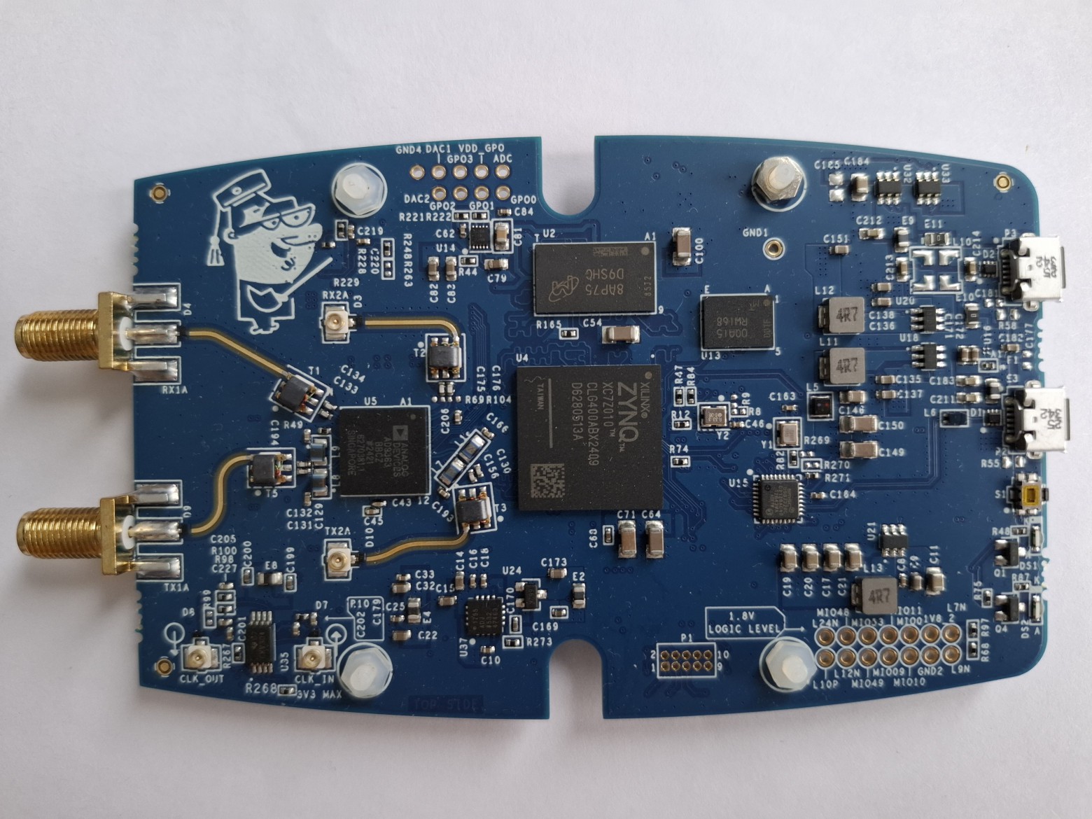
Fig. 1. General top view of the ADALM-PLUTO clone
So, we have a clone of a fairly popular SDR called ADALM-PLUTO and we need to write our own firmware for it. This clone differs from the original board in that it uses a slightly different FPGA — XC7Z010-CLG400. What does this mean for the firmware developer? And the fact that you will have to contact the seller and ask for a scheme. In this case, we were lucky, and the seller shared the .xdc file.
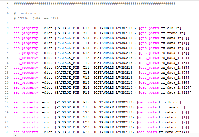
Fig. 2. A fragment of the provided .xdc file
There are many ways to create firmware for the ad936x and PlutoSDR, in particular. Here it is suggested to follow one of the simplest ones. There is such a resource https://wiki.analog.com . He can be very helpful in developing such software. For example, there is a page https://wiki.analog.com/resources/fpga/docs/build . Let’s go through these steps.
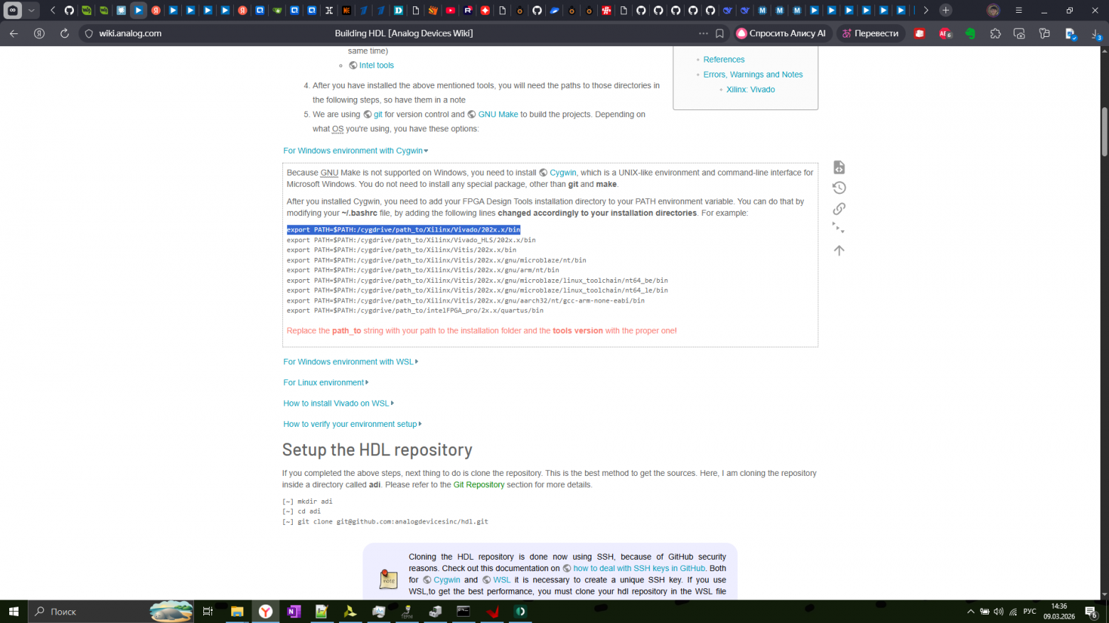
Figure 3. Screenshot of the Building HDL page
In this article, development will be carried out on a Windows system , so in CYGWIN we will execute the command
export PATH=$PATH:/cygdrive/C/Xilinx/Vivado/2021.1/bin
Please note that path_to has been replaced with C and the Vivado version is specified. After executing the which command , vivado returns the correct path to Vivado.
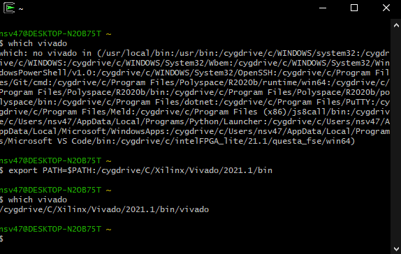
Fig. 4. Screenshot of Cygwin terminal
Now you can clone the repository and switch to the hdl_2021_r1 branch, because in this article the development is carried out using Vivado 2021.1.
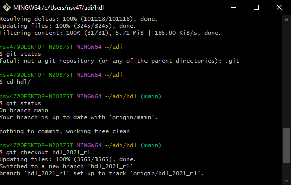
Fig. 5. Screenshot of the Git Bash terminal with the result of cloning and switching to a branch.
We are using a clone from another FPGA, so it is necessary to correct the sources. First of all , we 'll replace it .xdc on the provided one.
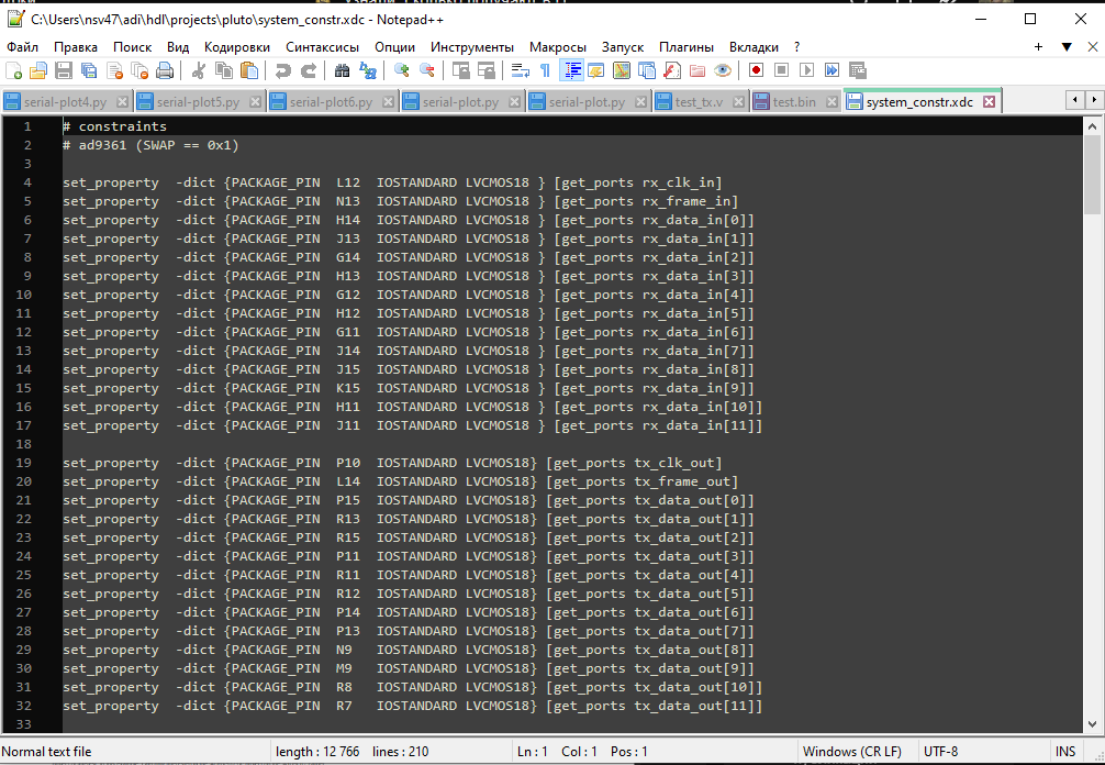
Fig. 6. Screenshot of a fragment of the original .xdc file
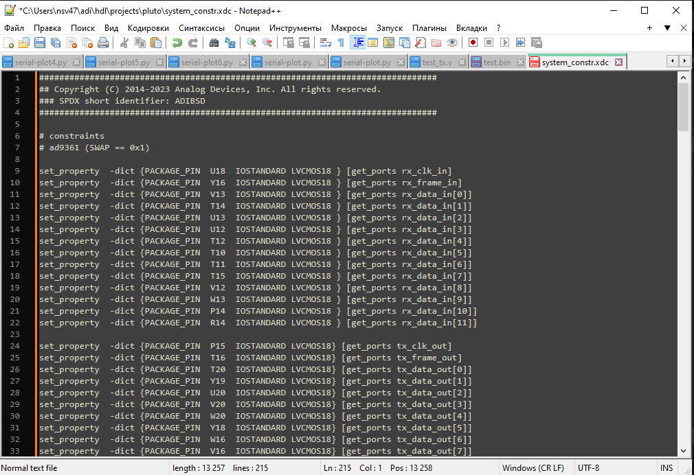
Fig. 7. Screenshot of a fragment of the .xdc substitution file
The two images above show that the destinations are different. For example, rx_clk_in was on L12, but it became on U18. In the system_bd.tcl file, on line 41, there is a parameter whose value must be replaced in accordance with the FPGA clone used on the board.
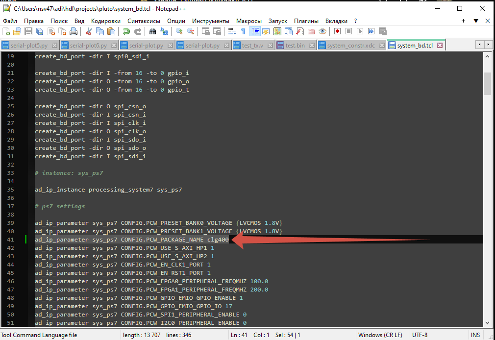
Figure 8. Screenshot of a fragment of the system_bd file.tcl with the changed parameter
In the system_project.tcl file, the FPGA model must be replaced on line 6.
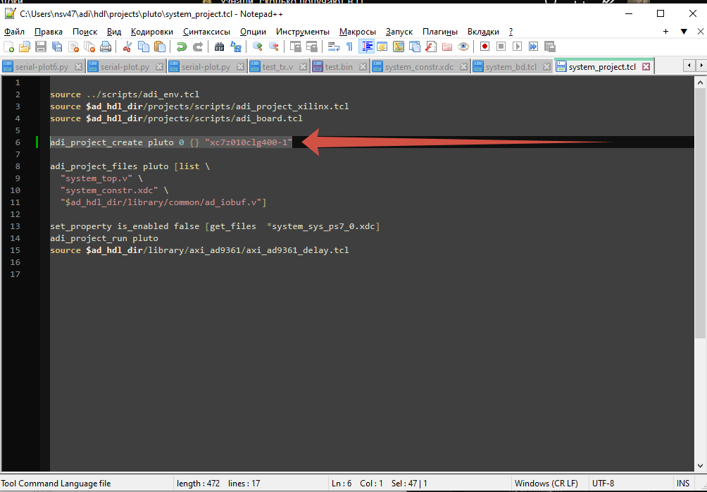
Fig. 9. Screenshot of a fragment of the system_project.tcl file with a modified FPGA model.
These are all changes that relate to hardware in terms of HDL design assembly.
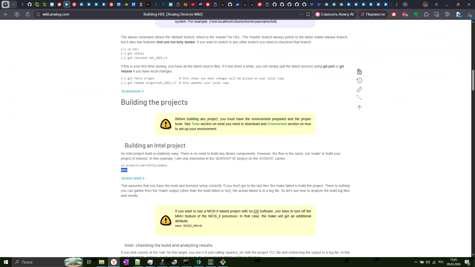
Fig. 10. Screenshot of the Building HDL page
Now, on the WIKI page, it is suggested to go to the required project and execute the make command. Please note that the make utility must be installed in Cygwin and the which make command must return the correct path, for example,
$ which make
/usr/bin/make
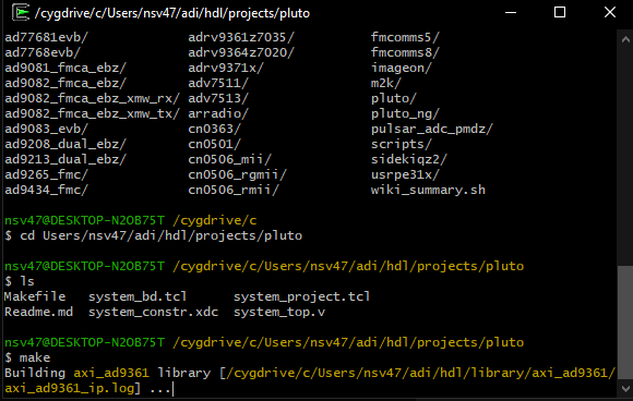
Fig. 11. Screenshot of the Cygwin terminal during the execution of the make command in the pluto project directory.
This process can be long. Relatively, for example, my old 2018 laptop, which was then with above-average hardware, now does it for about 20 minutes, and a PC with Ryzen9 from my old job built an fmcomms2 project for kc705 or zc706 in 10 minutes. By the way, the make execution process then suddenly and for some unknown reason ended with an error, then make can simply be started again and everything was going well.
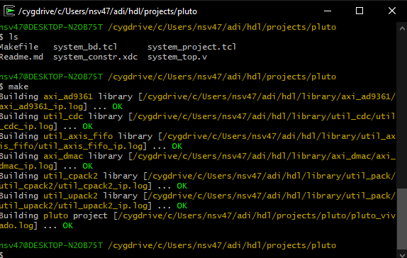
Fig. 12. Screenshot of Cygwin terminal with the results of make execution
The utility has completed its work, and now you can open the project using Vivado.
The project is really assembled for the necessary FPGA.
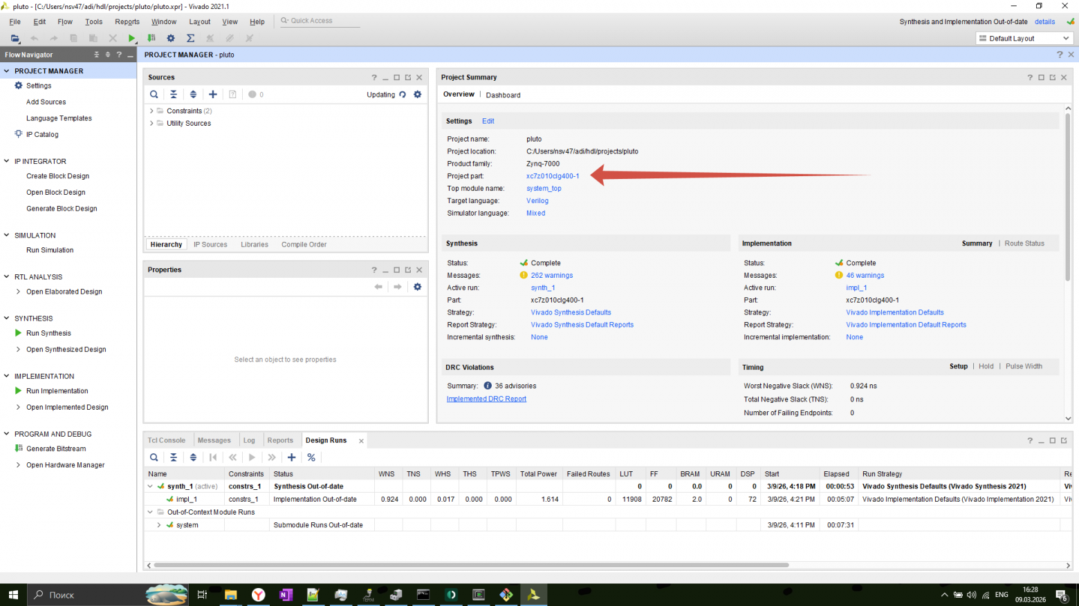
Fig. 13. Screenshot of the Vivado window with the FPGA used in the project.
And the new assignments are used according to the provided .xdc file.
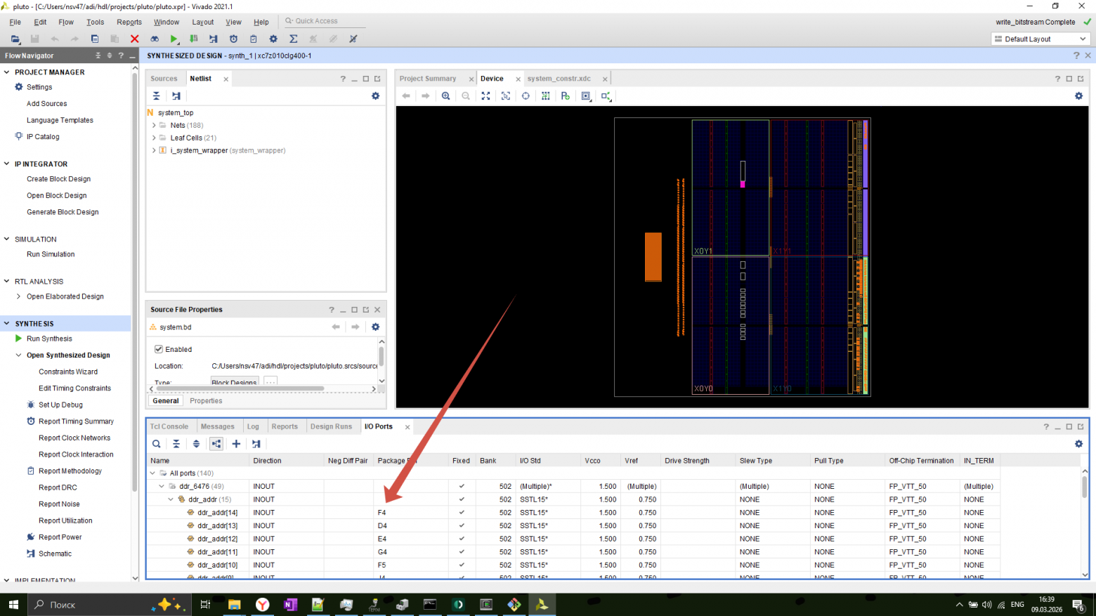
Fig. 14. Screenshot of the Vivado window.
At this stage, you can arrange an interim check and build a simple Hello World application that outputs information via UART. In this way, you can make sure that the HDL design is suitable for this board. For the Vitis application, you need to export hardware using File->Export->Export Hardware… Then the necessary .xsa file will appear in the specified directory.
Fig. 15. The Export Hardware Process
Pay attention to the Include bitstream option, this is important.
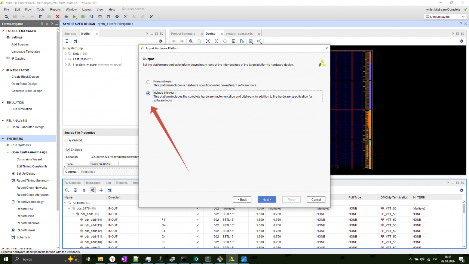
Fig. 16. It is necessary to select the correct option
Now you can open Vitis. Create a new application using File->New->Application Project…
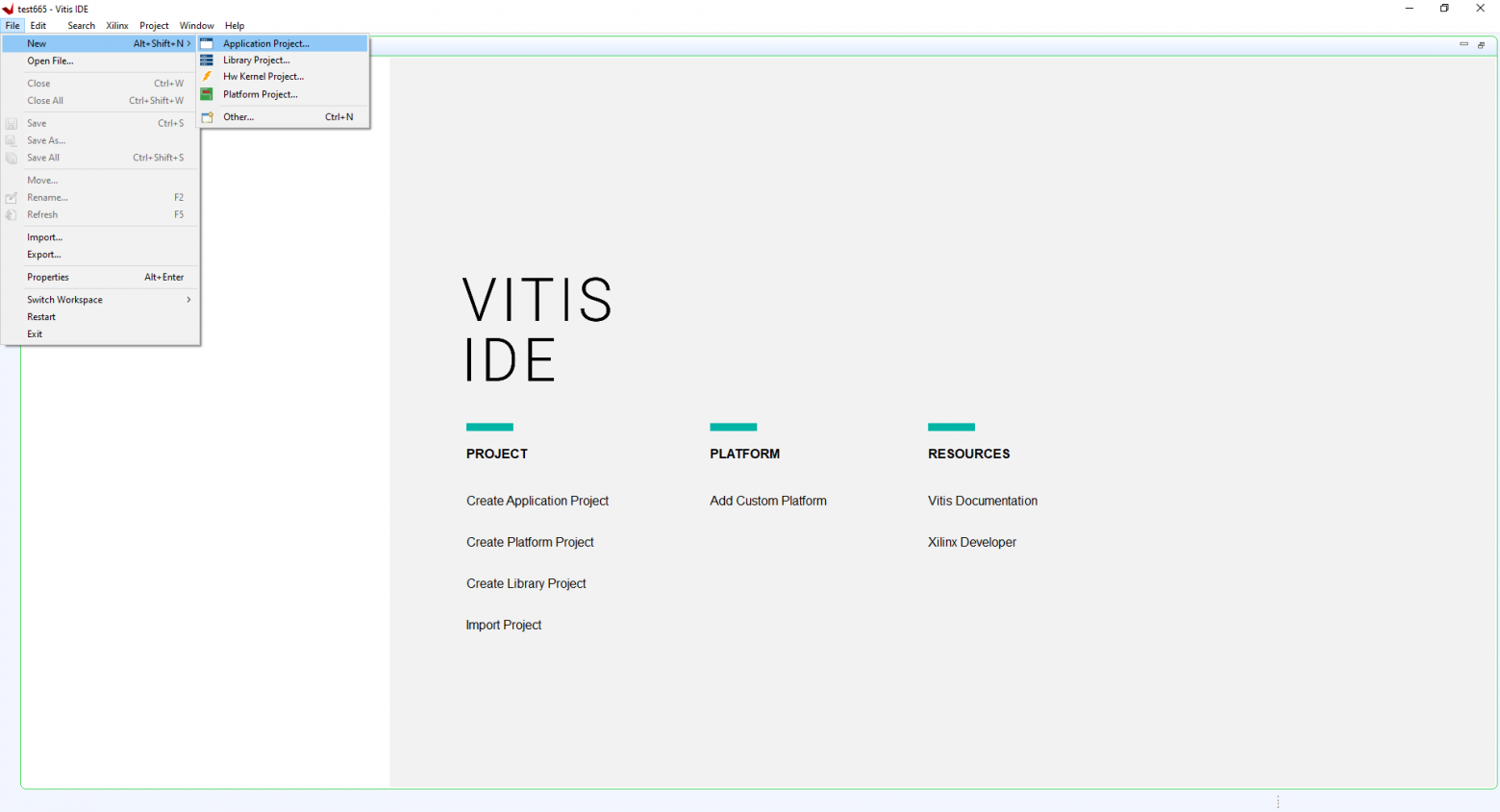
Fig. 17. Creating a new application
In the following stages, many things are intuitive. The main thing is to select the created one .xsa file:
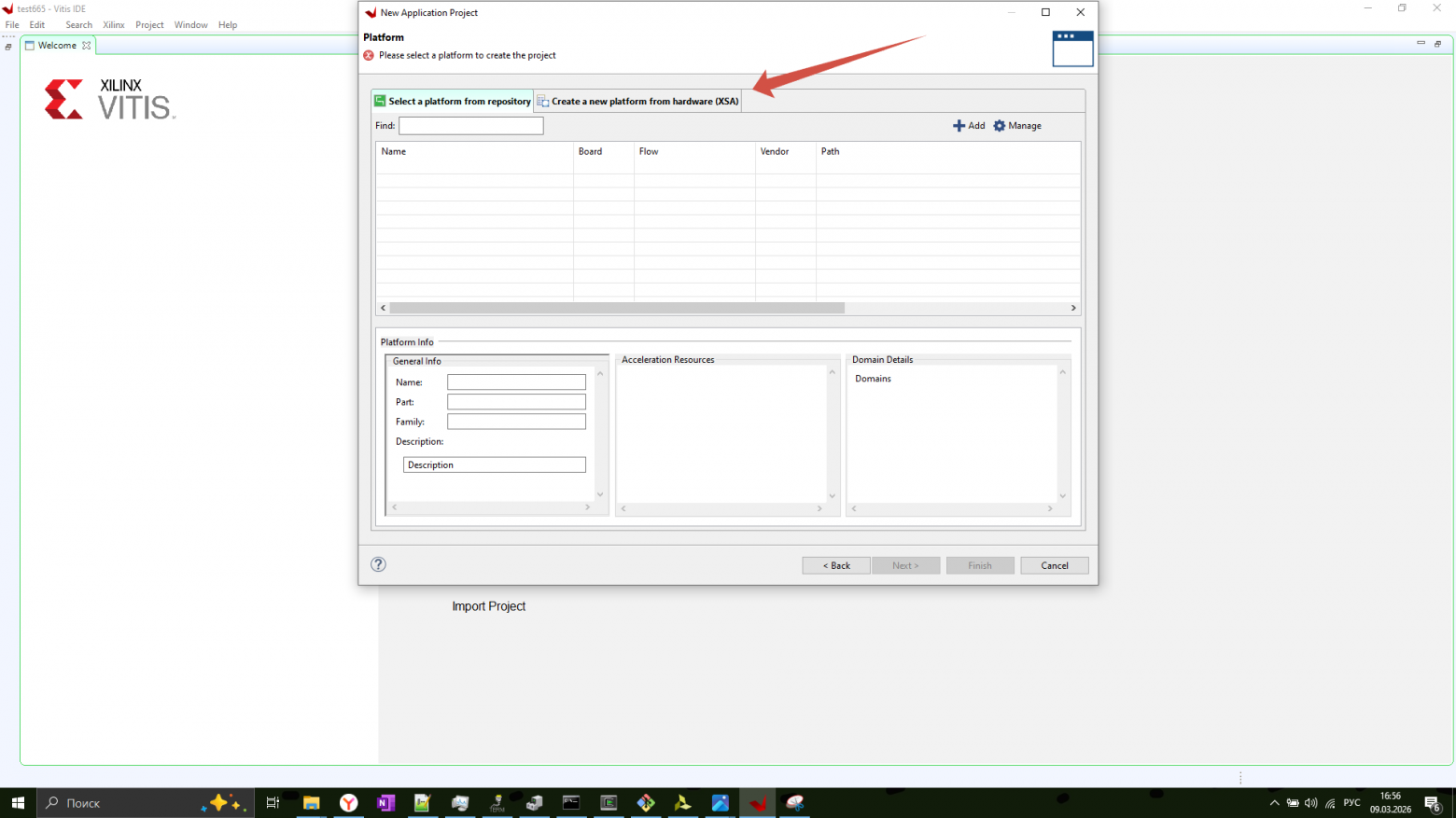
Fig. 18. Go to the Create from tab.xsa file
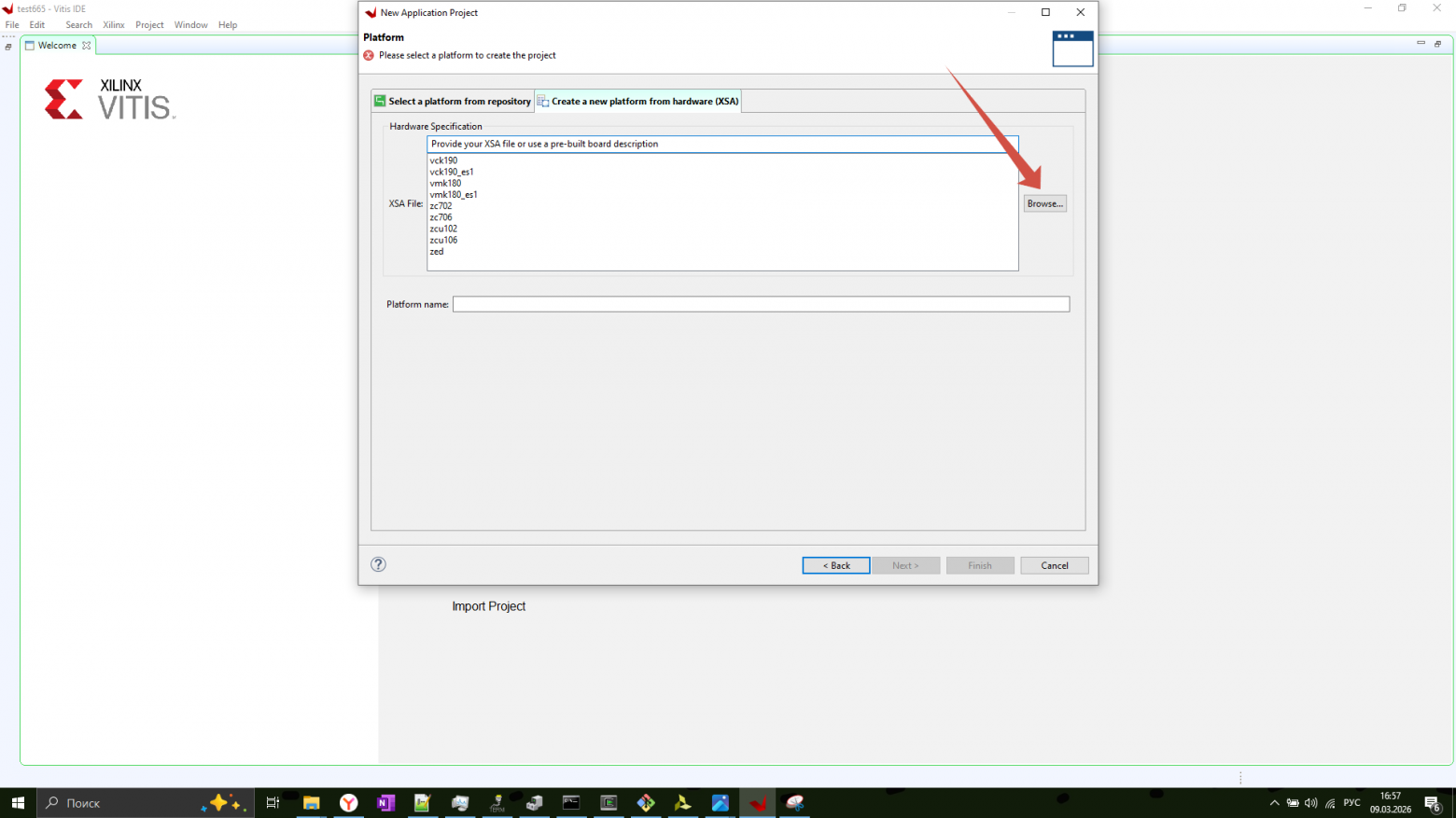
Fig. 19. And select the created one.xsa file
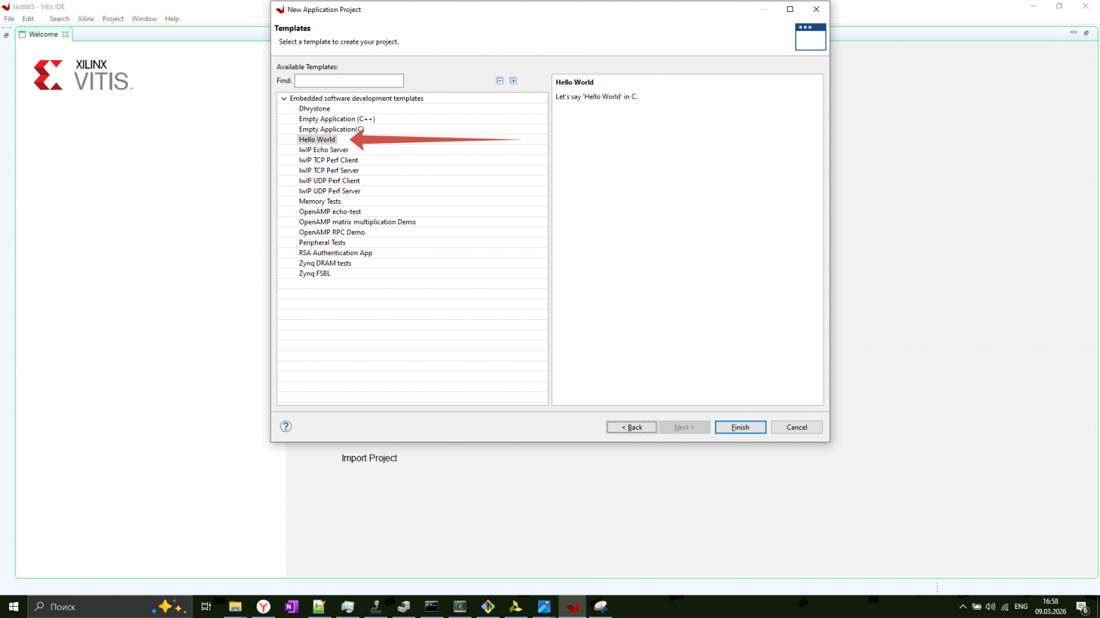
Fig. 20 Creating Hello World
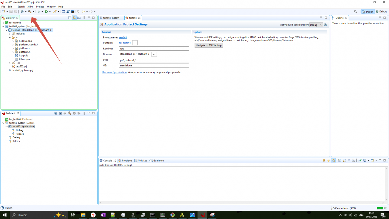
Fig. 21. Performing A Build
When the application is ready, we will face the question of how to download the firmware into the board. There is a page on wiki.analog https://wiki.analog.com/university/tools/pluto/devs/fpga but there is something indistinct written there. In any case, there are holes on the board for the FTSH connector.-105-01- L-D. It turned out to be a fairly rare connector, and it could not be found on sale. The description of the contacts is on the diagram, which is available on https://wiki.analog.com/university/tools/pluto/hacking/hardware . There are several revisions, but the JTAG is the same everywhere. By the way, you can use a relatively cheap Waveshare programmer to program Xilinx.
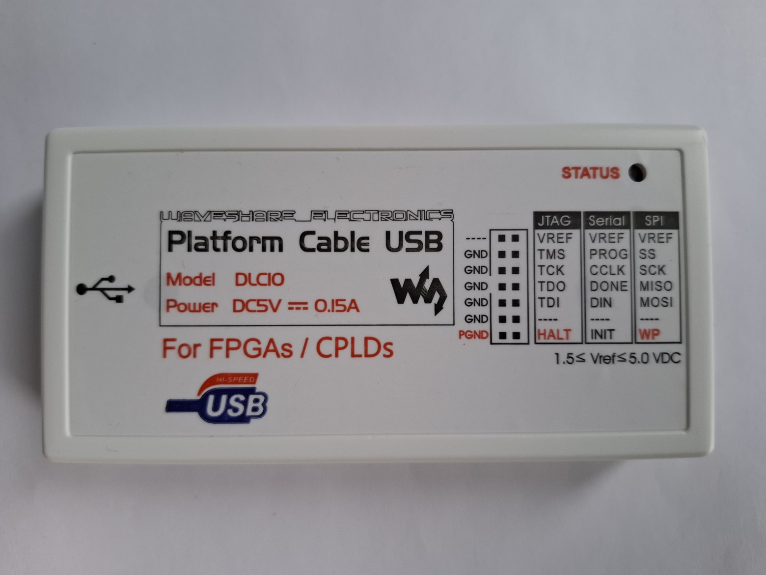
Fig. 22. One of the possible programmers
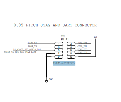
Fig. 23. Programmer connection diagram
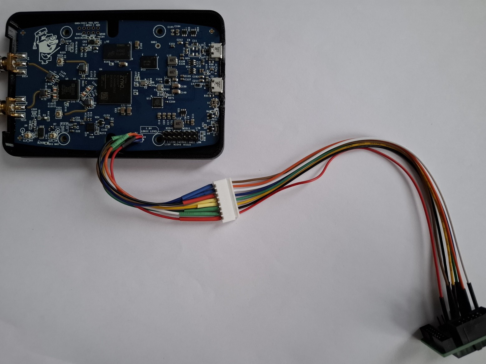
Fig. 24. Photo of a PlutoSDR clone with a soldered connector
We connect the programmer, then the outermost microUSB PlutoSDR, while the STATUS LED on the programmer turns green, the outermost LED lights up on the board, and a new COM port appears in the device manager. It is necessary to connect any convenient terminal to this COM port in order to see the UART output of the programmed card.
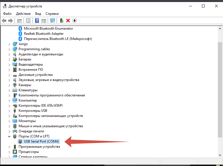
Fig. 25. PlutoSDR occupies COM port number 4.
When everything is connected, you need to return to Vitis and enter the Run Configurations menu.
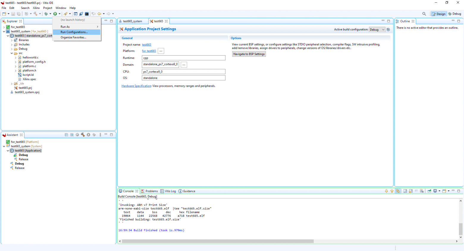
Fig. 26. Open the Run Configurations menu.
Double-click on System Project Debug and run Run.
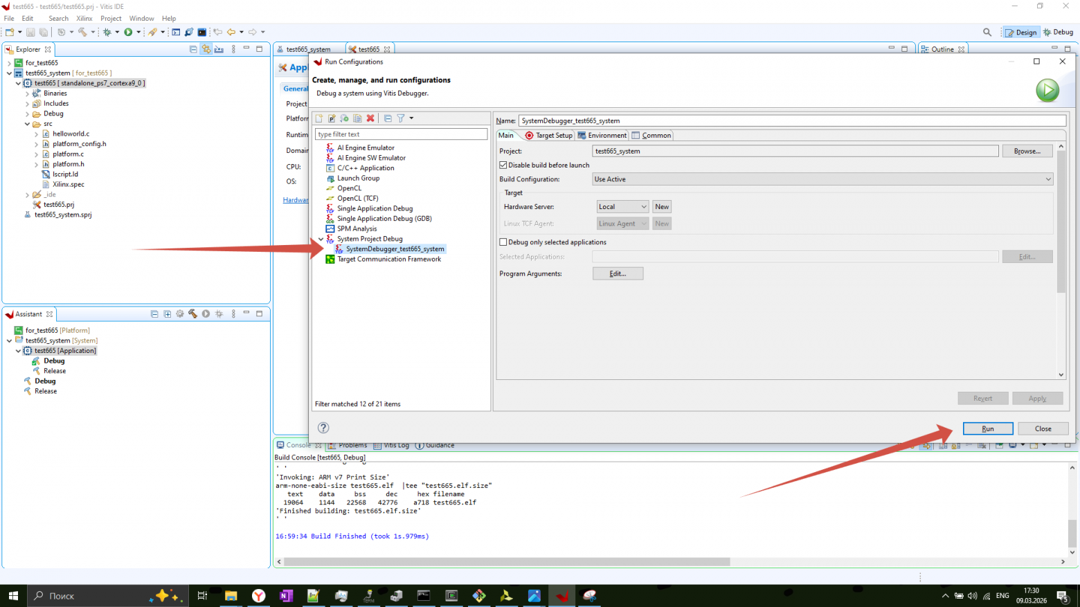
Fig. 27. We fill the firmware into the board.
Then the firmware download will begin, and when it is done, a message will appear in the terminal.
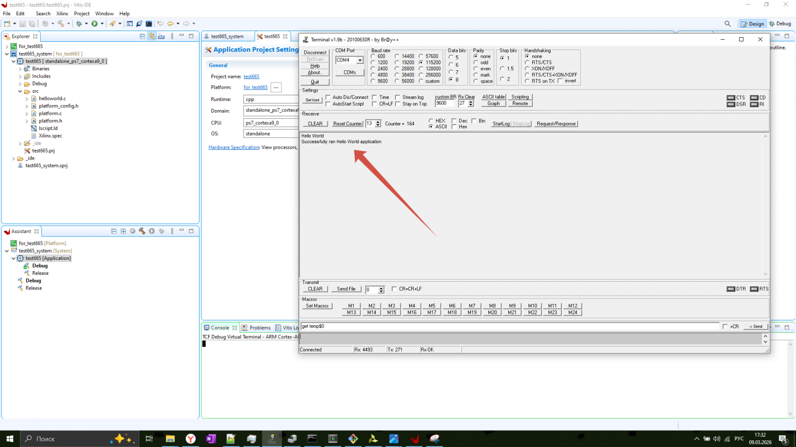
Fig. 28. The result of the program execution.
To summarize, there is a working HDL design that can be used to create applications and run them successfully. Let’s start creating an application for initializing and controlling the operation of the ad936x chip.
There are several ways to create a program for a microprocessor that will control the operation of the microcircuit, as in the case of creating an HDL design. Even there are at least two out-of-the-box microprocessors available. These are MicroBlaze and Zynq ARM cores. ADALM-PLUTO uses Zynq, as in the clone described in this article. Let’s turn to the page https://wiki.analog.com/resources/no-os/build . Open GIT BASH as an administrator and write the path to VItis using the command,
$ export PATH=$PATH:"/c/Xilinx/Vitis/2021.1/bi
Now the which command should return the path,
$ which vitis
/c/Xilinx/Vitis/2021.1/bin/vitis
You will need a compiler. At the time of writing, I managed to go in and download the latest available version from the link. If it was installed on the default path, then you can specify the path using the command
$ export PATH=$PATH:"/c/Program Files (x86)/GNU Arm Embedded Toolchain/10 2021.10/bin"
To check, you can view the version
$ arm-none-eabi-gcc --version
The no-OS repository must be cloned recursively.
git clone --recursive https://github.com/analogdevicesinc/no-OS
It took me a relatively long time. Don’t forget to switch to the 2021_R1 branch or the one you need. After that, you can copy the one you created earlier.the xsa file is in the root directory of the ad9361 project, and .It is better to rename the xsa file immediately to system_top.xsa, so as not to make a mistake later due to the features of the ready-made makefile. The app_config file.h needs to be edited. On line 47, there is a define that will select the chip we are using. But if you’re lucky, you can leave define on line 45. This is described on the page https://wiki.analog.com/university/tools/pluto/hacking/hardware . In this experiment, the define for ad9361 will remain, despite the fact that the ad9363 chip is soldered. Thus, this source code is suitable for the entire ad936x family.
I have already managed to use these sources to run both ad9361, ad9364, and now ad9363. It is only necessary to change the settings for a specific chip, for example, the ad9364 has one channel for receiving and transmitting. It’s working.
After that comes the define block, which are responsible for certain examples. To verify our work, we will analyze not only the debug information that is printed in the terminal. We will turn on a nearby transmitter that broadcasts a sinusoid, receive this signal on a Pluto with a bare-metal application, print the samples from the ADC into the terminal and build a graph from these samples. To do this, uncomment lines 55 with ADC_DMA_EXAMPLE, 57 with DAC_DMA_EXAMPLE, and 59 with TDD_SWITCH_STATE_EXAMPLE. Next, go to the main.c file. In this file, we are most interested in the default_init_param structure so far. On line 186, disable FDD mode (0, //frequency_division_duplex_mode_enable *** adi,frequency-division-duplex-mode-enable). On line 223, enable clocking from an external reference clock source (1, //xo_disable_use_ext_refclk_enable *** adi,xo-disable-use-ext-refclk-enable). On line 352, swap ports 0 and 1 (1, //swap_ports_enable *** adi,swap-ports-enable). On line 354, disable LVDS mode (0, //lvds_mode_enable *** adi,lvds-mode-enable). On line 357, enable the full_port_enable option (1, //full_port_enable *** adi,full-port-enable).
AD9361_InitParam default_init_param = {
	/* Device selection */
	ID_AD9361,	// dev_sel
	/* Reference Clock */
	40000000UL,	//reference_clk_rate
	/* Base Configuration */
	1,		//two_rx_two_tx_mode_enable *** adi,2rx-2tx-mode-enable
	1,		//one_rx_one_tx_mode_use_rx_num *** adi,1rx-1tx-mode-use-rx-num
	1,		//one_rx_one_tx_mode_use_tx_num *** adi,1rx-1tx-mode-use-tx-num
	0,		//frequency_division_duplex_mode_enable *** adi,frequency-division-duplex-mode-enable
	0,		//frequency_division_duplex_independent_mode_enable *** adi,frequency-division-duplex-independent-mode-enable
	0,		//tdd_use_dual_synth_mode_enable *** adi,tdd-use-dual-synth-mode-enable
	0,		//tdd_skip_vco_cal_enable *** adi,tdd-skip-vco-cal-enable
	0,		//tx_fastlock_delay_ns *** adi,tx-fastlock-delay-ns
	0,		//rx_fastlock_delay_ns *** adi,rx-fastlock-delay-ns
	0,		//rx_fastlock_pincontrol_enable *** adi,rx-fastlock-pincontrol-enable
	0,		//tx_fastlock_pincontrol_enable *** adi,tx-fastlock-pincontrol-enable
	0,		//external_rx_lo_enable *** adi,external-rx-lo-enable
	0,		//external_tx_lo_enable *** adi,external-tx-lo-enable
	5,		//dc_offset_tracking_update_event_mask *** adi,dc-offset-tracking-update-event-mask
	6,		//dc_offset_attenuation_high_range *** adi,dc-offset-attenuation-high-range
	5,		//dc_offset_attenuation_low_range *** adi,dc-offset-attenuation-low-range
	0x28,	//dc_offset_count_high_range *** adi,dc-offset-count-high-range
	0x32,	//dc_offset_count_low_range *** adi,dc-offset-count-low-range
	0,		//split_gain_table_mode_enable *** adi,split-gain-table-mode-enable
	MAX_SYNTH_FREF,	//trx_synthesizer_target_fref_overwrite_hz *** adi,trx-synthesizer-target-fref-overwrite-hz
	0,		// qec_tracking_slow_mode_enable *** adi,qec-tracking-slow-mode-enable
	/* ENSM Control */
	0,		//ensm_enable_pin_pulse_mode_enable *** adi,ensm-enable-pin-pulse-mode-enable
	0,		//ensm_enable_txnrx_control_enable *** adi,ensm-enable-txnrx-control-enable
	/* LO Control */
	2400000000UL,	//rx_synthesizer_frequency_hz *** adi,rx-synthesizer-frequency-hz
	2400000000UL,	//tx_synthesizer_frequency_hz *** adi,tx-synthesizer-frequency-hz
	1,				//tx_lo_powerdown_managed_enable *** adi,tx-lo-powerdown-managed-enable
	/* Rate & BW Control */
	{983040000, 245760000, 122880000, 61440000, 30720000, 30720000},// rx_path_clock_frequencies[6] *** adi,rx-path-clock-frequencies
	{983040000, 122880000, 122880000, 61440000, 30720000, 30720000},// tx_path_clock_frequencies[6] *** adi,tx-path-clock-frequencies
	18000000,//rf_rx_bandwidth_hz *** adi,rf-rx-bandwidth-hz
	18000000,//rf_tx_bandwidth_hz *** adi,rf-tx-bandwidth-hz
	/* RF Port Control */
	0,		//rx_rf_port_input_select *** adi,rx-rf-port-input-select
	0,		//tx_rf_port_input_select *** adi,tx-rf-port-input-select
	/* TX Attenuation Control */
	10000,	//tx_attenuation_mdB *** adi,tx-attenuation-mdB
	0,		//update_tx_gain_in_alert_enable *** adi,update-tx-gain-in-alert-enable
	/* Reference Clock Control */
	1,		//xo_disable_use_ext_refclk_enable *** adi,xo-disable-use-ext-refclk-enable
	{8, 5920},	//dcxo_coarse_and_fine_tune[2] *** adi,dcxo-coarse-and-fine-tune
	CLKOUT_DISABLE,	//clk_output_mode_select *** adi,clk-output-mode-select
	/* Gain Control */
	2,		//gc_rx1_mode *** adi,gc-rx1-mode
	2,		//gc_rx2_mode *** adi,gc-rx2-mode
	58,		//gc_adc_large_overload_thresh *** adi,gc-adc-large-overload-thresh
	4,		//gc_adc_ovr_sample_size *** adi,gc-adc-ovr-sample-size
	47,		//gc_adc_small_overload_thresh *** adi,gc-adc-small-overload-thresh
	8192,	//gc_dec_pow_measurement_duration *** adi,gc-dec-pow-measurement-duration
	0,		//gc_dig_gain_enable *** adi,gc-dig-gain-enable
	800,	//gc_lmt_overload_high_thresh *** adi,gc-lmt-overload-high-thresh
	704,	//gc_lmt_overload_low_thresh *** adi,gc-lmt-overload-low-thresh
	24,		//gc_low_power_thresh *** adi,gc-low-power-thresh
	15,		//gc_max_dig_gain *** adi,gc-max-dig-gain
	0,		//gc_use_rx_fir_out_for_dec_pwr_meas_enable *** adi,gc-use-rx-fir-out-for-dec-pwr-meas-enable
	/* Gain MGC Control */
	2,		//mgc_dec_gain_step *** adi,mgc-dec-gain-step
	2,		//mgc_inc_gain_step *** adi,mgc-inc-gain-step
	0,		//mgc_rx1_ctrl_inp_enable *** adi,mgc-rx1-ctrl-inp-enable
	0,		//mgc_rx2_ctrl_inp_enable *** adi,mgc-rx2-ctrl-inp-enable
	0,		//mgc_split_table_ctrl_inp_gain_mode *** adi,mgc-split-table-ctrl-inp-gain-mode
	/* Gain AGC Control */
	10,		//agc_adc_large_overload_exceed_counter *** adi,agc-adc-large-overload-exceed-counter
	2,		//agc_adc_large_overload_inc_steps *** adi,agc-adc-large-overload-inc-steps
	0,		//agc_adc_lmt_small_overload_prevent_gain_inc_enable *** adi,agc-adc-lmt-small-overload-prevent-gain-inc-enable
	10,		//agc_adc_small_overload_exceed_counter *** adi,agc-adc-small-overload-exceed-counter
	4,		//agc_dig_gain_step_size *** adi,agc-dig-gain-step-size
	3,		//agc_dig_saturation_exceed_counter *** adi,agc-dig-saturation-exceed-counter
	1000,	// agc_gain_update_interval_us *** adi,agc-gain-update-interval-us
	0,		//agc_immed_gain_change_if_large_adc_overload_enable *** adi,agc-immed-gain-change-if-large-adc-overload-enable
	0,		//agc_immed_gain_change_if_large_lmt_overload_enable *** adi,agc-immed-gain-change-if-large-lmt-overload-enable
	10,		//agc_inner_thresh_high *** adi,agc-inner-thresh-high
	1,		//agc_inner_thresh_high_dec_steps *** adi,agc-inner-thresh-high-dec-steps
	12,		//agc_inner_thresh_low *** adi,agc-inner-thresh-low
	1,		//agc_inner_thresh_low_inc_steps *** adi,agc-inner-thresh-low-inc-steps
	10,		//agc_lmt_overload_large_exceed_counter *** adi,agc-lmt-overload-large-exceed-counter
	2,		//agc_lmt_overload_large_inc_steps *** adi,agc-lmt-overload-large-inc-steps
	10,		//agc_lmt_overload_small_exceed_counter *** adi,agc-lmt-overload-small-exceed-counter
	5,		//agc_outer_thresh_high *** adi,agc-outer-thresh-high
	2,		//agc_outer_thresh_high_dec_steps *** adi,agc-outer-thresh-high-dec-steps
	18,		//agc_outer_thresh_low *** adi,agc-outer-thresh-low
	2,		//agc_outer_thresh_low_inc_steps *** adi,agc-outer-thresh-low-inc-steps
	1,		//agc_attack_delay_extra_margin_us; *** adi,agc-attack-delay-extra-margin-us
	0,		//agc_sync_for_gain_counter_enable *** adi,agc-sync-for-gain-counter-enable
	/* Fast AGC */
	64,		//fagc_dec_pow_measuremnt_duration ***  adi,fagc-dec-pow-measurement-duration
	260,	//fagc_state_wait_time_ns ***  adi,fagc-state-wait-time-ns
	/* Fast AGC - Low Power */
	0,		//fagc_allow_agc_gain_increase ***  adi,fagc-allow-agc-gain-increase-enable
	5,		//fagc_lp_thresh_increment_time ***  adi,fagc-lp-thresh-increment-time
	1,		//fagc_lp_thresh_increment_steps ***  adi,fagc-lp-thresh-increment-steps
	/* Fast AGC - Lock Level (Lock Level is set via slow AGC inner high threshold) */
	1,		//fagc_lock_level_lmt_gain_increase_en ***  adi,fagc-lock-level-lmt-gain-increase-enable
	5,		//fagc_lock_level_gain_increase_upper_limit ***  adi,fagc-lock-level-gain-increase-upper-limit
	/* Fast AGC - Peak Detectors and Final Settling */
	1,		//fagc_lpf_final_settling_steps ***  adi,fagc-lpf-final-settling-steps
	1,		//fagc_lmt_final_settling_steps ***  adi,fagc-lmt-final-settling-steps
	3,		//fagc_final_overrange_count ***  adi,fagc-final-overrange-count
	/* Fast AGC - Final Power Test */
	0,		//fagc_gain_increase_after_gain_lock_en ***  adi,fagc-gain-increase-after-gain-lock-enable
	/* Fast AGC - Unlocking the Gain */
	0,		//fagc_gain_index_type_after_exit_rx_mode ***  adi,fagc-gain-index-type-after-exit-rx-mode
	1,		//fagc_use_last_lock_level_for_set_gain_en ***  adi,fagc-use-last-lock-level-for-set-gain-enable
	1,		//fagc_rst_gla_stronger_sig_thresh_exceeded_en ***  adi,fagc-rst-gla-stronger-sig-thresh-exceeded-enable
	5,		//fagc_optimized_gain_offset ***  adi,fagc-optimized-gain-offset
	10,		//fagc_rst_gla_stronger_sig_thresh_above_ll ***  adi,fagc-rst-gla-stronger-sig-thresh-above-ll
	1,		//fagc_rst_gla_engergy_lost_sig_thresh_exceeded_en ***  adi,fagc-rst-gla-engergy-lost-sig-thresh-exceeded-enable
	1,		//fagc_rst_gla_engergy_lost_goto_optim_gain_en ***  adi,fagc-rst-gla-engergy-lost-goto-optim-gain-enable
	10,		//fagc_rst_gla_engergy_lost_sig_thresh_below_ll ***  adi,fagc-rst-gla-engergy-lost-sig-thresh-below-ll
	8,		//fagc_energy_lost_stronger_sig_gain_lock_exit_cnt ***  adi,fagc-energy-lost-stronger-sig-gain-lock-exit-cnt
	1,		//fagc_rst_gla_large_adc_overload_en ***  adi,fagc-rst-gla-large-adc-overload-enable
	1,		//fagc_rst_gla_large_lmt_overload_en ***  adi,fagc-rst-gla-large-lmt-overload-enable
	0,		//fagc_rst_gla_en_agc_pulled_high_en ***  adi,fagc-rst-gla-en-agc-pulled-high-enable
	0,		//fagc_rst_gla_if_en_agc_pulled_high_mode ***  adi,fagc-rst-gla-if-en-agc-pulled-high-mode
	64,		//fagc_power_measurement_duration_in_state5 ***  adi,fagc-power-measurement-duration-in-state5
	2,		//fagc_large_overload_inc_steps *** adi,fagc-adc-large-overload-inc-steps
	/* RSSI Control */
	1,		//rssi_delay *** adi,rssi-delay
	1000,	//rssi_duration *** adi,rssi-duration
	3,		//rssi_restart_mode *** adi,rssi-restart-mode
	0,		//rssi_unit_is_rx_samples_enable *** adi,rssi-unit-is-rx-samples-enable
	1,		//rssi_wait *** adi,rssi-wait
	/* Aux ADC Control */
	256,	//aux_adc_decimation *** adi,aux-adc-decimation
	40000000UL,	//aux_adc_rate *** adi,aux-adc-rate
	/* AuxDAC Control */
	1,		//aux_dac_manual_mode_enable ***  adi,aux-dac-manual-mode-enable
	0,		//aux_dac1_default_value_mV ***  adi,aux-dac1-default-value-mV
	0,		//aux_dac1_active_in_rx_enable ***  adi,aux-dac1-active-in-rx-enable
	0,		//aux_dac1_active_in_tx_enable ***  adi,aux-dac1-active-in-tx-enable
	0,		//aux_dac1_active_in_alert_enable ***  adi,aux-dac1-active-in-alert-enable
	0,		//aux_dac1_rx_delay_us ***  adi,aux-dac1-rx-delay-us
	0,		//aux_dac1_tx_delay_us ***  adi,aux-dac1-tx-delay-us
	0,		//aux_dac2_default_value_mV ***  adi,aux-dac2-default-value-mV
	0,		//aux_dac2_active_in_rx_enable ***  adi,aux-dac2-active-in-rx-enable
	0,		//aux_dac2_active_in_tx_enable ***  adi,aux-dac2-active-in-tx-enable
	0,		//aux_dac2_active_in_alert_enable ***  adi,aux-dac2-active-in-alert-enable
	0,		//aux_dac2_rx_delay_us ***  adi,aux-dac2-rx-delay-us
	0,		//aux_dac2_tx_delay_us ***  adi,aux-dac2-tx-delay-us
	/* Temperature Sensor Control */
	256,	//temp_sense_decimation *** adi,temp-sense-decimation
	1000,	//temp_sense_measurement_interval_ms *** adi,temp-sense-measurement-interval-ms
	0xCE,	//temp_sense_offset_signed *** adi,temp-sense-offset-signed
	1,		//temp_sense_periodic_measurement_enable *** adi,temp-sense-periodic-measurement-enable
	/* Control Out Setup */
	0xFF,	//ctrl_outs_enable_mask *** adi,ctrl-outs-enable-mask
	0,		//ctrl_outs_index *** adi,ctrl-outs-index
	/* External LNA Control */
	0,		//elna_settling_delay_ns *** adi,elna-settling-delay-ns
	0,		//elna_gain_mdB *** adi,elna-gain-mdB
	0,		//elna_bypass_loss_mdB *** adi,elna-bypass-loss-mdB
	0,		//elna_rx1_gpo0_control_enable *** adi,elna-rx1-gpo0-control-enable
	0,		//elna_rx2_gpo1_control_enable *** adi,elna-rx2-gpo1-control-enable
	0,		//elna_gaintable_all_index_enable *** adi,elna-gaintable-all-index-enable
	/* Digital Interface Control */
	0,		//digital_interface_tune_skip_mode *** adi,digital-interface-tune-skip-mode
	0,		//digital_interface_tune_fir_disable *** adi,digital-interface-tune-fir-disable
	1,		//pp_tx_swap_enable *** adi,pp-tx-swap-enable
	1,		//pp_rx_swap_enable *** adi,pp-rx-swap-enable
	0,		//tx_channel_swap_enable *** adi,tx-channel-swap-enable
	0,		//rx_channel_swap_enable *** adi,rx-channel-swap-enable
	1,		//rx_frame_pulse_mode_enable *** adi,rx-frame-pulse-mode-enable
	0,		//two_t_two_r_timing_enable *** adi,2t2r-timing-enable
	0,		//invert_data_bus_enable *** adi,invert-data-bus-enable
	0,		//invert_data_clk_enable *** adi,invert-data-clk-enable
	0,		//fdd_alt_word_order_enable *** adi,fdd-alt-word-order-enable
	0,		//invert_rx_frame_enable *** adi,invert-rx-frame-enable
	0,		//fdd_rx_rate_2tx_enable *** adi,fdd-rx-rate-2tx-enable
	1,		//swap_ports_enable *** adi,swap-ports-enable
	0,		//single_data_rate_enable *** adi,single-data-rate-enable
	0,		//lvds_mode_enable *** adi,lvds-mode-enable
	0,		//half_duplex_mode_enable *** adi,half-duplex-mode-enable
	0,		//single_port_mode_enable *** adi,single-port-mode-enable
	1,		//full_port_enable *** adi,full-port-enable
	0,		//full_duplex_swap_bits_enable *** adi,full-duplex-swap-bits-enable
	0,		//delay_rx_data *** adi,delay-rx-data
	0,		//rx_data_clock_delay *** adi,rx-data-clock-delay
	4,		//rx_data_delay *** adi,rx-data-delay
	7,		//tx_fb_clock_delay *** adi,tx-fb-clock-delay
	0,		//tx_data_delay *** adi,tx-data-delay
#ifdef ALTERA_PLATFORM
	300,	//lvds_bias_mV *** adi,lvds-bias-mV
#else
	150,	//lvds_bias_mV *** adi,lvds-bias-mV
#endif
	1,		//lvds_rx_onchip_termination_enable *** adi,lvds-rx-onchip-termination-enable
	0,		//rx1rx2_phase_inversion_en *** adi,rx1-rx2-phase-inversion-enable
	0xFF,	//lvds_invert1_control *** adi,lvds-invert1-control
	0x0F,	//lvds_invert2_control *** adi,lvds-invert2-control
	/* GPO Control */
	0,		//gpo_manual_mode_enable *** adi,gpo-manual-mode-enable
	0,		//gpo_manual_mode_enable_mask *** adi,gpo-manual-mode-enable-mask
	0,		//gpo0_inactive_state_high_enable *** adi,gpo0-inactive-state-high-enable
	0,		//gpo1_inactive_state_high_enable *** adi,gpo1-inactive-state-high-enable
	0,		//gpo2_inactive_state_high_enable *** adi,gpo2-inactive-state-high-enable
	0,		//gpo3_inactive_state_high_enable *** adi,gpo3-inactive-state-high-enable
	0,		//gpo0_slave_rx_enable *** adi,gpo0-slave-rx-enable
	0,		//gpo0_slave_tx_enable *** adi,gpo0-slave-tx-enable
	0,		//gpo1_slave_rx_enable *** adi,gpo1-slave-rx-enable
	0,		//gpo1_slave_tx_enable *** adi,gpo1-slave-tx-enable
	0,		//gpo2_slave_rx_enable *** adi,gpo2-slave-rx-enable
	0,		//gpo2_slave_tx_enable *** adi,gpo2-slave-tx-enable
	0,		//gpo3_slave_rx_enable *** adi,gpo3-slave-rx-enable
	0,		//gpo3_slave_tx_enable *** adi,gpo3-slave-tx-enable
	0,		//gpo0_rx_delay_us *** adi,gpo0-rx-delay-us
	0,		//gpo0_tx_delay_us *** adi,gpo0-tx-delay-us
	0,		//gpo1_rx_delay_us *** adi,gpo1-rx-delay-us
	0,		//gpo1_tx_delay_us *** adi,gpo1-tx-delay-us
	0,		//gpo2_rx_delay_us *** adi,gpo2-rx-delay-us
	0,		//gpo2_tx_delay_us *** adi,gpo2-tx-delay-us
	0,		//gpo3_rx_delay_us *** adi,gpo3-rx-delay-us
	0,		//gpo3_tx_delay_us *** adi,gpo3-tx-delay-us
	/* Tx Monitor Control */
	37000,	//low_high_gain_threshold_mdB *** adi,txmon-low-high-thresh
	0,		//low_gain_dB *** adi,txmon-low-gain
	24,		//high_gain_dB *** adi,txmon-high-gain
	0,		//tx_mon_track_en *** adi,txmon-dc-tracking-enable
	0,		//one_shot_mode_en *** adi,txmon-one-shot-mode-enable
	511,	//tx_mon_delay *** adi,txmon-delay
	8192,	//tx_mon_duration *** adi,txmon-duration
	2,		//tx1_mon_front_end_gain *** adi,txmon-1-front-end-gain
	2,		//tx2_mon_front_end_gain *** adi,txmon-2-front-end-gain
	48,		//tx1_mon_lo_cm *** adi,txmon-1-lo-cm
	48,		//tx2_mon_lo_cm *** adi,txmon-2-lo-cm
	/* GPIO definitions */
	{
		.number = -1,
		.platform_ops = GPIO_OPS,
		.extra = GPIO_PARAM
	},		//gpio_resetb *** reset-gpios
	/* MCS Sync */
	{
		.number = -1,
		.platform_ops = GPIO_OPS,
		.extra = GPIO_PARAM
	},		//gpio_sync *** sync-gpios

	{
		.number = -1,
		.platform_ops = GPIO_OPS,
		.extra = GPIO_PARAM
	},		//gpio_cal_sw1 *** cal-sw1-gpios

	{
		.number = -1,
		.platform_ops = GPIO_OPS,
		.extra = GPIO_PARAM
	},		//gpio_cal_sw2 *** cal-sw2-gpios

	{
		.device_id = SPI_DEVICE_ID,
		.mode = NO_OS_SPI_MODE_1,
		.chip_select = SPI_CS,
		.platform_ops = SPI_OPS,
		.extra = SPI_PARAM
	},

	/* External LO clocks */
	NULL,	//(*ad9361_rfpll_ext_recalc_rate)()
	NULL,	//(*ad9361_rfpll_ext_round_rate)()
	NULL,	//(*ad9361_rfpll_ext_set_rate)()
#ifndef AXI_ADC_NOT_PRESENT
	&rx_adc_init,	// *rx_adc_init
	&tx_dac_init,   // *tx_dac_init
#endif
};
At the same time, in order to output samples to the terminal, it is necessary to add lines to the last block of the TDD_SWITCH_STATE_EXAMPLE example code, which, for convenience, will output the received signal level to the terminal, then read the data from the DMA, the data will be checked, and 1024 samples from the channel we need will be output in a cycle. This happens on line 21 in the code below. That is, there are only 4 channels, i0, q0, i1, q1. And according to this condition, samples from one channel will be printed.
struct rf_rssi ch0;
struct rf_rssi ch1;

ad9361_get_rx_rssi(ad9361_phy, 0, &ch0);
ad9361_get_rx_rssi(ad9361_phy, 1, &ch1);
printf("ch0: %lu %lu %lu %ld %d\n", ch0.ant, ch0.symbol, ch0.preamble, ch0.multiplier, ch0.duration);
printf("ch1: %lu %lu %lu %ld %d\n", ch1.ant, ch1.symbol, ch1.preamble, ch1.multiplier, ch1.duration);

/* Read the data from the ADC DMA. */
axi_dmac_transfer_start(rx_dmac, &read_transfer);

/* Wait until transfer finishes */
status = axi_dmac_transfer_wait_completion(rx_dmac, 500);
if(status < 0)
    return status;

Xil_DCacheInvalidateRange((uintptr_t)adc_buffer, sizeof(adc_buffer));

//----------------------------------------------------------------------------------------------------
for(int i = 0; i < 4096; i++){
    if(i%4==0){
        int16_t sample = (int16_t)adc_buffer[i];
        printf("%d\n", sample);
    }
}
//----------------------------------------------------------------------------------------------------
In Git Bash, run the mac command in the ad9361 project directory.
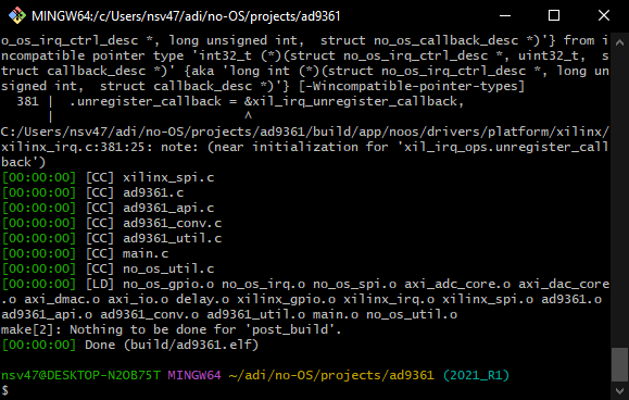
Fig. 29. Screenshot of the GIT BASH terminal after making a make
The terminal will display some debugging information about the processes of building, linking and compiling the project, and some warnings that can be ignored for now. And at the end there will be information about the successful creation of a binary file for our microprocessor. Let’s see what happens if you upload the program to ZYNQ. To do this, you need to add commands to the terminal:
export XSCT_REMOTE_HOST=127.0.0.1
export XSCT_REMOTE_PORT=3121
This is also written on https://wiki.analog.com/resources/no-os/build in the Running/Debugging section. We connect the programmer, if we have already managed to turn it off, and power the debugging board. We check the COM port on which the PlutoSDR clone is sitting and connect to the com port with our favorite terminal at a speed of 115200. In Git Bash, we write the make run command.
At the first firmware update, after connecting the programmer, it turns itself off a couple of times and connects to the system. And in Git Bash, information appears about an allegedly successful download, although this is not the case. I just ignore it and run the command again.
By the way, if you export from Vivado .You didn’t name the xsa file system_top.xsa, then you can get couldn’t open <path_do_Your_bit>: no such file or directory
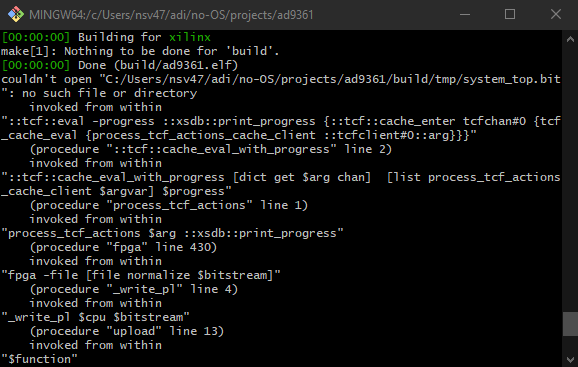
Fig. 30. Screenshot of the Git Bash terminal when system_top.bit cannot be found
It’s not a big deal, you just need to rename your _Yours>.bit in system_top.bit and run make run again. And this time, the blue LED on the debugging board will flash with a bright blue light, and the cherished message will be output to the COM port d9361_init : AD936x Rev 2 successfully initialized. But the information in the terminal is not complete.
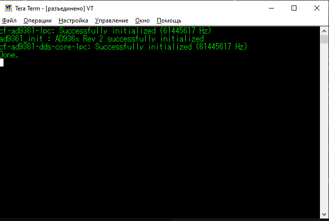
Fig 31. Screenshot of the COM terminal with debugging information from the ad936x chip.
Not all of it, because when running only the DMA_EXAMPLE example, DAC_DMA_EXAMPLE: address=0x161030 samples=65536 channels=4 bits=16 should be printed to the terminal. This can be seen in the source code on line 812.
printf("DAC_DMA_EXAMPLE: address=%#lx samples=%lu channels=%u bits=%lu\n",
	       (uintptr_t)adc_buffer, NO_OS_ARRAY_SIZE(adc_buffer), rx_adc_init.num_channels,
	       8 * sizeof(adc_buffer[0]));
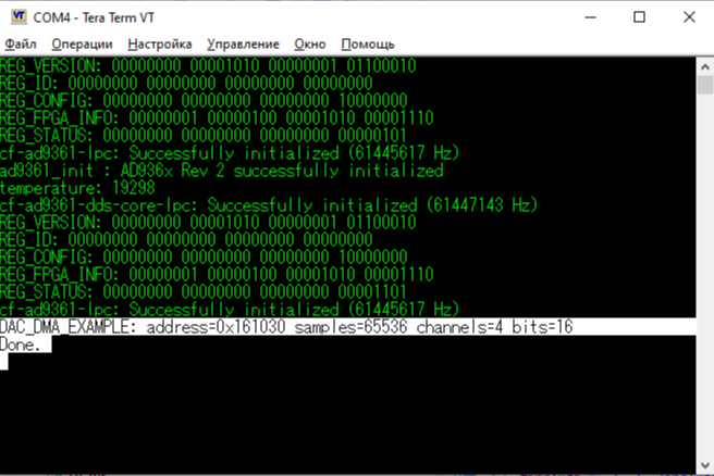
Fig. 32. Screenshot of the COM terminal with information about the executed TDD_SWITCH_STATE_EXAMPLE example.
I noticed this when I first started programming these chips a few years ago. Debugging without an IDE didn’t seem very convenient to me, so I switched to Vitis. Since then, I have not started building applications in the Git Bash terminal. And I didn’t look for this bug, most likely, I need to pick at the makefile. Maybe someone will do it and share it in the comments.
Let’s build this app in Vitis. It all starts exactly the same as Hello World, but you need to create an empty app.
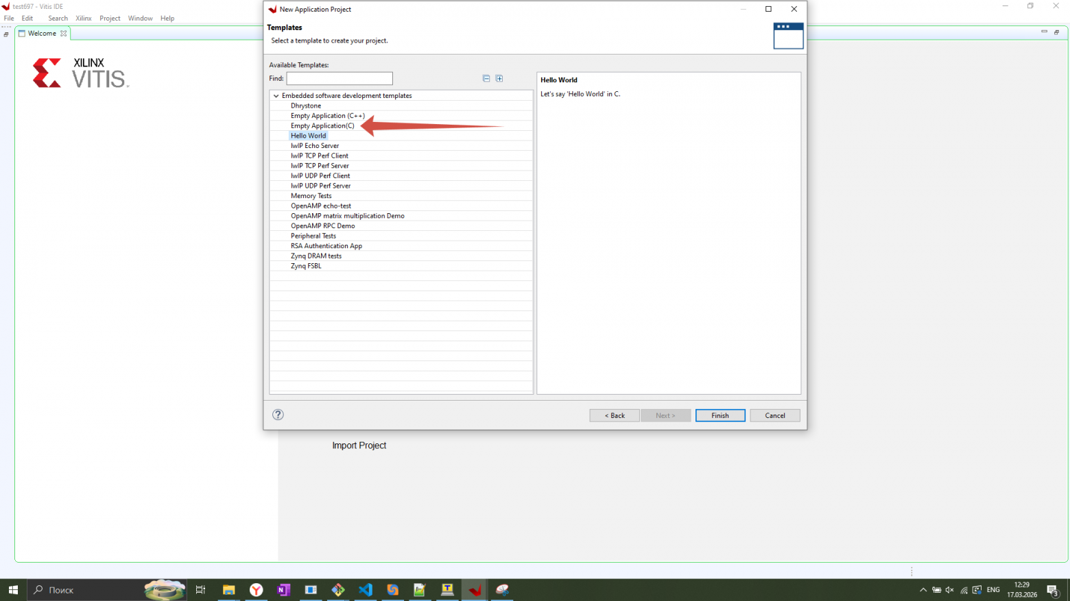
Fig. 33. The process of creating an Empty application
And then you need to add all the necessary source files.
They are available on Github
I added the source files that I used a lot on Github. But it’s better to double-check them. Because there is extra debugging information being displayed somewhere.
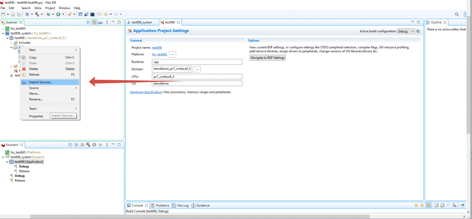
Fig. 34. Importing sources to Vitis.
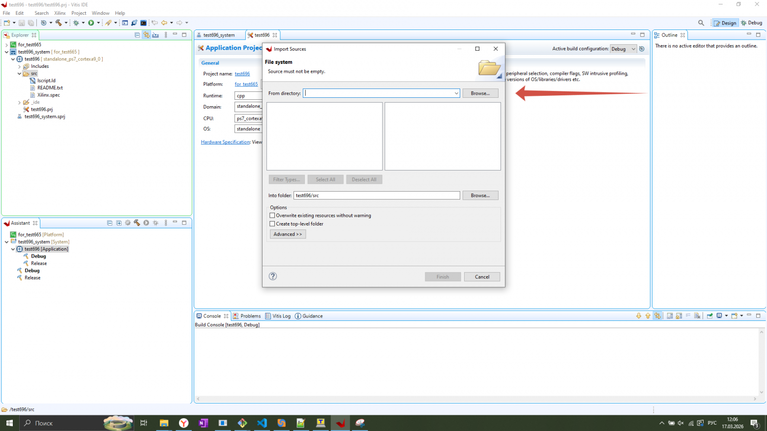
Fig. 35. Importing sources to Vitis.
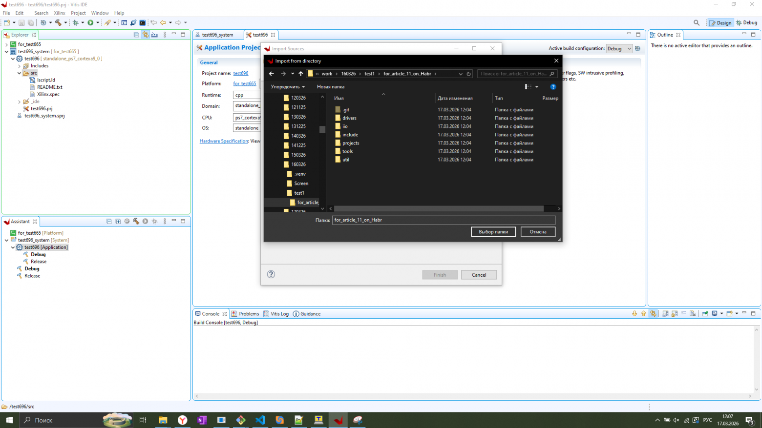
Fig. 36. Importing sources to Vitis.
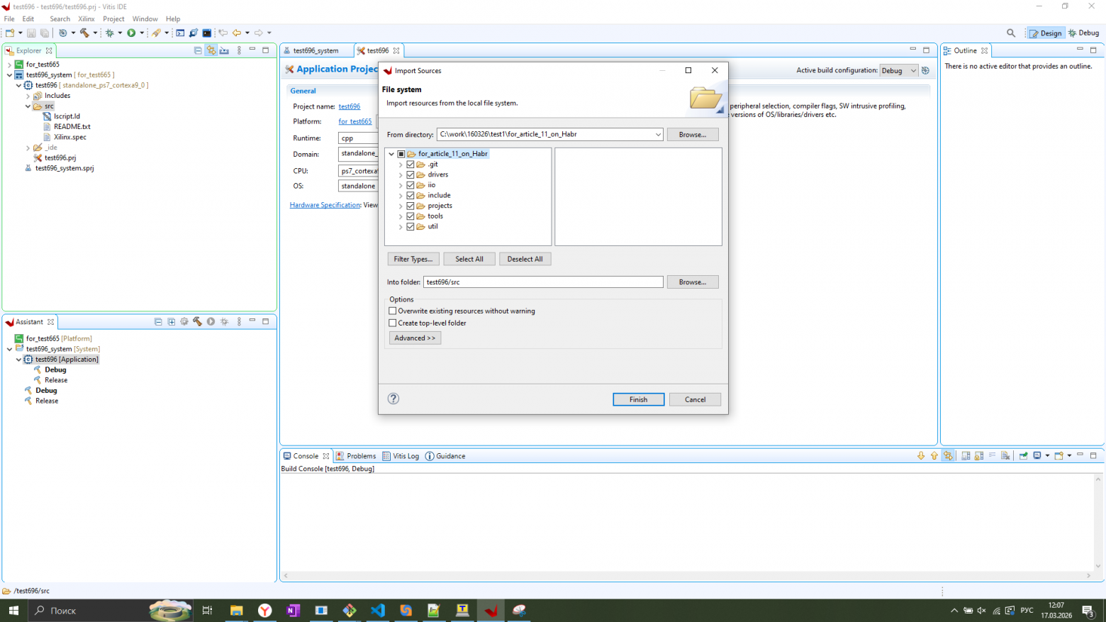
Fig. 37. Importing sources to Vitis.
After adding it, you need to do a Build, but the IDE doesn’t really like the paths, so they need to be rewritten.
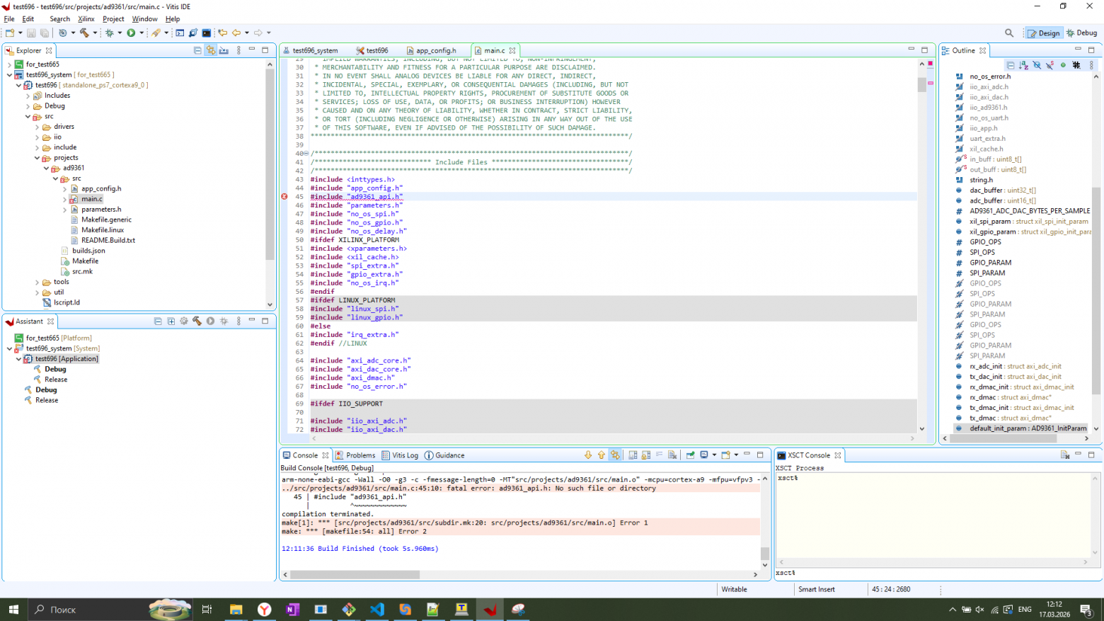
Fig. 38. Errors due to paths.
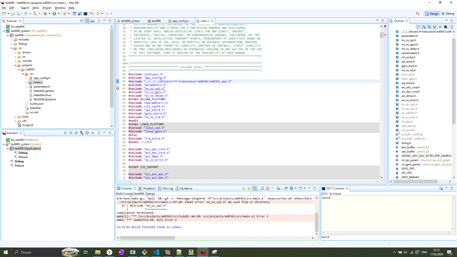
Fig. 39. Errors due to paths.
When all the paths are fixed, everything completes without errors.
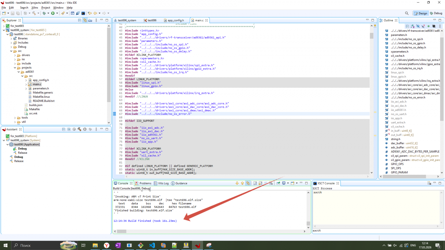
Figure 40. Successful build and compilation.
Now, if you include all the necessary examples that we discussed earlier, the values of the samples on the required channel will be printed to the terminal.
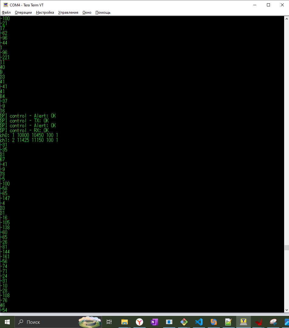
Fig. 41. Signal level when the sine generator is turned off
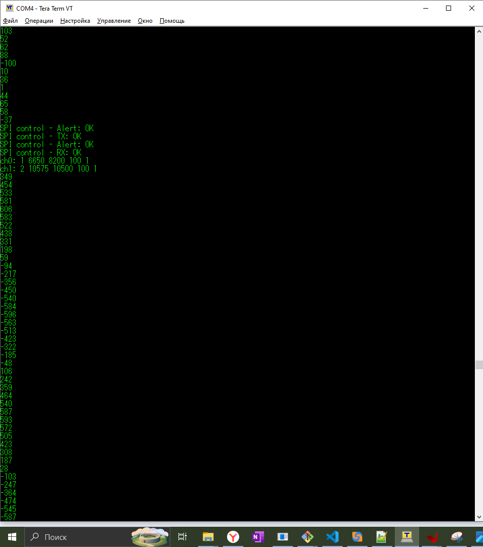
Fig. 42. Signal level when the sine generator is turned on at 0 dBm
To build a graph from the counts, you can copy them to a file and use a very simple Python script.
import numpy as np
from matplotlib import pyplot as plt

# Reading data from a file
with open('data2.txt', 'r') as f:
    data = [int(line.strip()) for line in f.readlines()]

# Drawing a graph
plt.figure(figsize=(12, 6))
plt.plot(data, 'b-', linewidth=0.5)
plt.xlabel('Saples')
plt.ylabel('Value')
plt.title('Data from data1.txt')
plt.grid(True, alpha=0.3)
plt.axhline(y=0, color='r', linestyle='--', alpha=0.5)
plt.show()
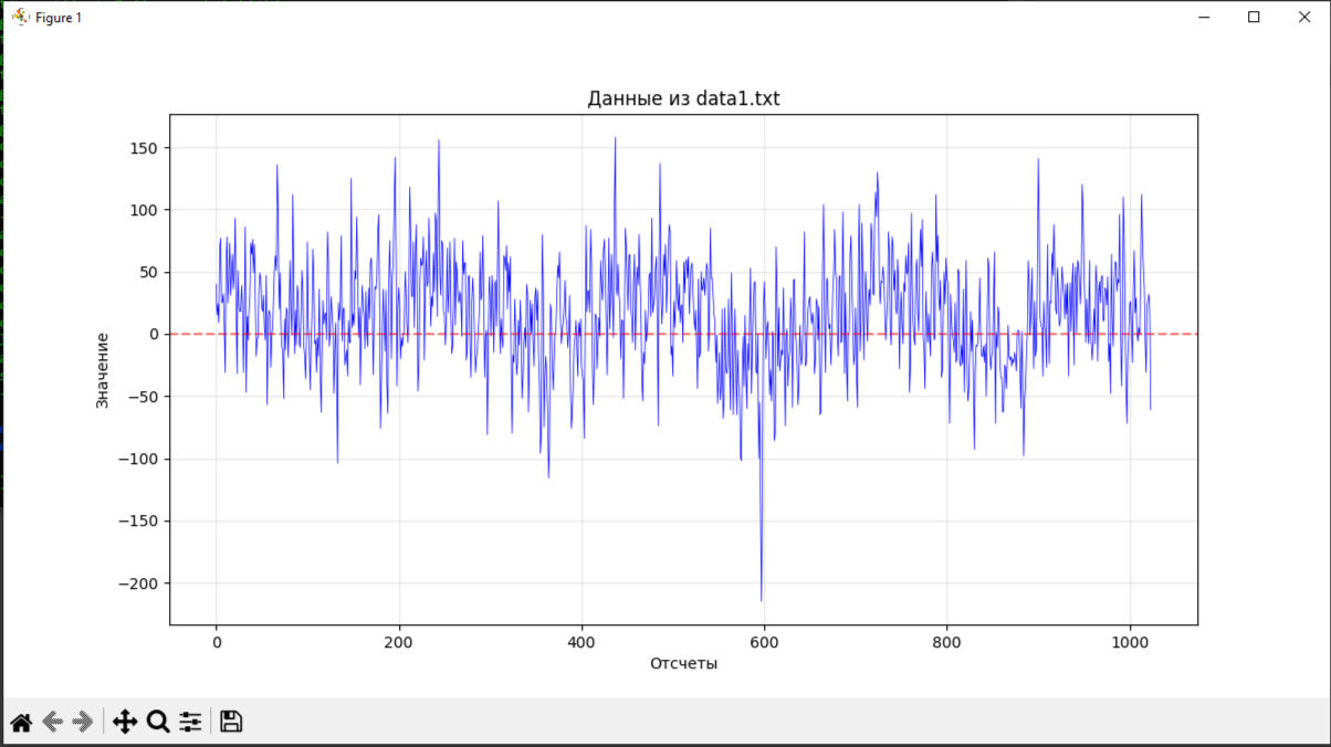
Fig 43. Some noise at 2.4 GHz with the generator turned off
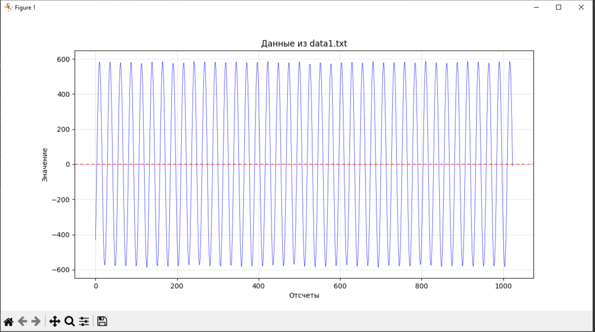
Fig 44. The sine from the generator at 2.4012 GHz.
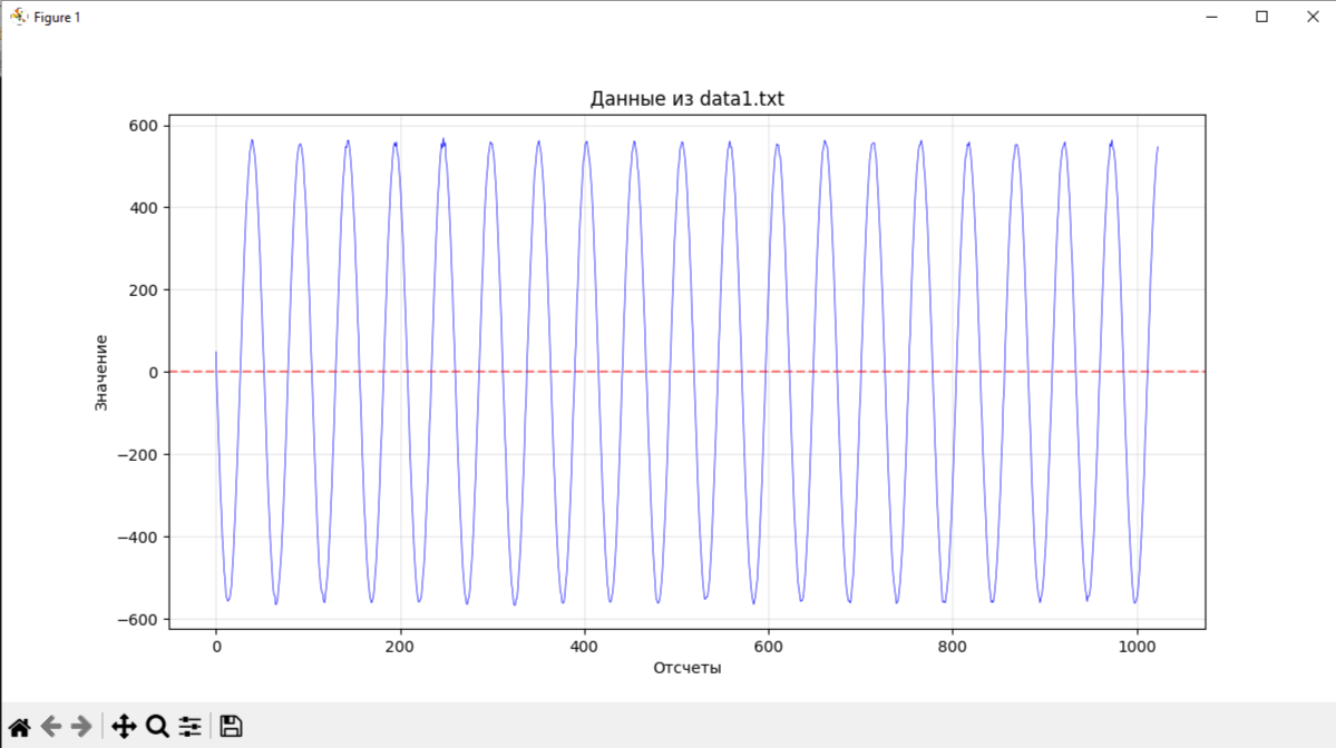
Fig 45. The sine from the generator at 2.4006 GHz.
Let’s summarize the results. What does it all mean? This means that the chip has received SPI from the ARM core, which we have successfully programmed into our registers the necessary data for initialization and operation in reception and transmission modes. The built-in state machine controls the chip via SPI and switches it alternately into reception and transmission modes. The axi_ad9361 core is initialized and outputs data that you and I can read through DMA and print with this implementation. A lot of songs of praise have been sung about the ad9361, it is a chip that deserves respect, but the threshold for entry without studying examples remains relatively high.
For a long time, I have been plagued by errors in the initialization of the axi_ad9361 kernel. The AD9361_InitParam structure contains the digital_interface_tune_skip_mode parameter, which must be activated with a certain HDL design. Moreover, even with the reference design, you may stumble upon unexpected errors, for example, if you configure the Digital Interface Control incorrectly, a message will be printed to the terminal under the spoiler below.
cf-ad9361-lpc: Successfully initialized (61445617 Hz)
SAMPL CLK: 30720000 tuning: RX
  0:1:2:3:4:5:6:7:8:9:a:b:c:d:e:f:
0:# # # # # # # # # # # # # # # #
1:# # # # # # # # # # # # # # # #
ad9361_dig_tune_delay: Tuning RX FAILED!
ad9361_init : AD936x initialization error
And the first thing you want to do is skip setting up the digital interface. Then there will even be a message about the initialization of the chip and HDL cores, but this is a direct road to a dead end when developing for ad9361. Errors in setting up the digital interface directly indicate information transmission problems, and they cannot be ignored!
This article is a drop in the ocean of registers and the sea of possibilities of the ad9361. And if you’re interested, we could talk in future articles about using this chip to transmit various data, whether it’s symbols for transmitting messages or even simple video transmission using a bare-metal application.
Therefore, please feel free to ask your questions in the comments. Even if I can’t answer them, maybe people who are more deeply immersed in using this chip will see it.
Thank you.
S. N.
Discussions
Become a Hackaday.io Member
Create an account to leave a comment. Already have an account? Log In.