-
How PCB Hole Copper Thickness Affects Your Soldering Process
5 days ago • 0 commentsWhen designing printed circuit boards (PCBs), most hobbyists and engineers focus on the component layout, routing, and overall design. But one aspect that is often overlooked—yet can significantly impact the quality of your work—is PCB hole copper thickness. While it might not be the first thing that comes to mind, the copper thickness in the PCB's holes plays a crucial role in the soldering process. In this article, we'll dive into why copper thickness matters, how it affects soldering, and what to consider when choosing the right copper thickness for your projects.
What Is PCB Hole Copper Thickness?
First, let’s quickly define what we're talking about. In a PCB, holes are created for through-hole components, vias, and sometimes even for mounting. These holes are plated with copper to create electrical connections between different layers of the board. The copper thickness refers to the amount of copper plating inside the hole, which is critical for ensuring the electrical integrity and mechanical stability of these connections.
Why Copper Thickness Matters for Soldering
Copper thickness inside PCB holes directly impacts the thermal properties and electrical conductivity of the connection. This, in turn, has several important effects on the soldering process:
1. Heat Dissipation During Soldering
When soldering, heat is applied to the metal pads and the surrounding PCB area. The copper inside the hole acts as a heat sink, drawing heat away from the solder joint. If the copper is too thin, it might not be able to absorb and dissipate the heat efficiently, leading to the following issues:
- Cold Solder Joints: If the heat isn’t adequately transferred, solder might not flow well, leading to poor joints.
- Soldering Irons Working Harder: Thin copper can cause prolonged heating times, increasing the likelihood of damaging components or the PCB itself.
- Small, low-power components: These typically don't require heavy copper, and standard copper thickness should be sufficient.
- High-current or large components (e.g., power transistors): These will benefit from heavier copper thickness to ensure the joints can handle the power demands.
2. Mechanical Strength of the Joint
The copper plating in the hole isn’t just there for electrical conductivity—it also plays a role in the mechanical integrity of the solder joint. A thicker copper layer creates a stronger, more robust bond between the component lead and the PCB. Without enough copper thickness, the joint may lack sufficient mechanical support, leading to potential reliability issues, especially in high-vibration or high-stress environments (think automotive or industrial applications).
3. Current Carrying Capacity
For designs that involve high current or power electronics, the copper thickness inside the PCB holes is crucial to prevent thermal runaway or poor conductivity. A thicker copper layer inside the hole ensures the joint can handle more current without excessive heat buildup, reducing the risk of failure. For standard consumer electronics, this is less of a concern, but in high-power circuits, this could be the difference between a project that works for a few hours and one that lasts for years.
4. Solder Flow and Wettability
The ability of solder to flow into the hole is essential for creating a solid electrical connection. A thicker copper layer can sometimes create more resistance to the solder’s flow, especially if it’s not adequately heated or if the hole is too large. Conversely, too thin a copper layer may cause solder to poorly adhere or create weak bonds. Proper balance is key!
How to Choose the Right Copper Thickness for Your PCB Design
Now that we understand the importance of copper thickness in PCB holes, how do you go about choosing the right one for your project? The decision depends on several factors, including the type of components you're using, the power requirements, and the expected stresses on the board....
Read more -
Copper-Based Superconductors: The Key to Next-Gen High-Performance PCBs
03/27/2026 at 08:25 • 0 comments
As the demand for more powerful, efficient, and compact electronic devices continues to rise, the need for advanced materials in PCB (Printed Circuit Board)design has never been greater. One material that has recently gained significant attention in the electronics community is copper-based superconductors. These materials are poised to play a pivotal role in the evolution of high-performance PCBs, providing solutions to issues like power loss, heat dissipation, and signal integrity.
In this article, we’ll explore how copper-based superconductors can be a game-changer for PCB technology, the science behind these materials, and their potential applications in next-gen electronics.
What Are Copper-Based Superconductors?
Superconductivity is a phenomenon where a material can conduct electricity with zero resistance when cooled below a certain critical temperature. This means that, unlike conventional conductors like copper or aluminum, superconducting materials do not waste energy as heat when current flows through them.
Traditional PCBs rely on materials like copper for conducting electrical signals. While copper is a great conductor at room temperature, it still faces challenges in high-frequency applications or situations where power dissipation becomes a bottleneck. Copper-based superconductors, on the other hand, offer the potential to eliminate these issues. By using copper in a superconducting state, engineers can create PCBs that are not only faster and more efficient but also more reliable.
Why Copper-Based Superconductors?
Copper has long been favored for its low resistivity and cost-effectiveness, making it an ideal material for most conventional PCBs. However, at high frequencies or in power-hungry devices, copper begins to suffer from a phenomenon called skin effect, where higher frequency currents tend to concentrate near the surface of the conductor, leading to energy losses and heat buildup.
Superconductors, however, have no electrical resistance, so there is no loss of energy as heat. When copper is used in a superconducting state, it can theoretically handle higher frequencies and carry larger amounts of current without the loss of energy associated with traditional copper conductors. This makes copper-based superconductors an ideal material for next-generation, high-performance PCBs, especially in high-power or high-frequency applications like RF (Radio Frequency) circuits, quantum computing, and advanced telecommunications.
Key Benefits of Copper-Based Superconductors in PCB Design:
- Zero Energy Loss: By eliminating resistance, copper-based superconductors can prevent energy loss in the form of heat, significantly improving power efficiency.
- Enhanced Signal Integrity: Superconductivity helps maintain the quality of high-frequency signals by reducing attenuation and distortion, which is critical in applications like high-speed communications and RF circuitry.
- Better Heat Dissipation: In conventional PCBs, power loss leads to heat buildup, which can damage components or degrade performance. Copper-based superconductors, by virtue of having zero resistance, don’t produce heat, helping to maintain the integrity of sensitive components.
- Improved Performance in Extreme Conditions: Superconducting copper alloys can perform better in harsh environments, such as extreme temperatures or high-radiation conditions, where traditional materials might fail.
- Miniaturization: The ability to handle higher frequencies and power loads without generating heat means that designers can create smaller, more compact PCBs. This is crucial for the miniaturization of modern electronics, including wearable devices, medical implants, and small-scale quantum computers.
The Science Behind Copper-Based Superconductors
While copper itself is not a superconductor at standard temperatures, it can be made superconducting under certain conditions, typically by introducing other elements or compounds into the...
Read more -
When PCB Peelable Soldermask Goes Wrong: 7 Fab Mistakes to Avoid
03/20/2026 at 08:39 • 0 comments
If you’ve spent any time around PCB fab, rework benches, or low-volume assembly, you already know peelable soldermask is one of those materials that looks almost too simple to screw up. Apply it, keep solder off the wrong spots, peel it away, move on.
Except that’s not always how it goes.
Used properly, PCB peelable soldermask is a handy temporary mask for protecting gold fingers, test pads, vias, connectors, and other no-solder zones during wave soldering, selective soldering, hand soldering, rework, or surface finishing. Unlike permanent LPI soldermask, it’s there for one job: shield the area, survive the process, then come off cleanly.
That makes it one of those shop-floor materials that lives somewhere between solid process engineering and a sticky little hack that saves the batch.
And when it goes wrong, it usually doesn’t fail in some exotic, chemistry-lab way. It fails because of ordinary process mistakes—applied too thin, cured too fast, used on dirty surfaces, or trusted where it shouldn’t be.
Here are seven of the most common ways peelable soldermask turns from a useful process aid into a production headache.
1. Applying PCB Peelable Soldermask Too Thin
This is the most common failure mode, and probably the easiest one to underestimate.
A lot of operators treat peelable soldermask like paint: just enough to tint the surface, and that should be fine. The trouble is, peelable soldermask isn’t there to look covered—it’s there to form a continuous protective film. If the layer is too thin, it may not seal the area properly, and it definitely won’t peel the way you want.
Instead of lifting off in one satisfying strip, it tears, shreds, or leaves behind little islands of material in exactly the places you were trying to protect.
What goes wrong
A thin application can lead to:
- Pinholes or incomplete coverage
- Solder intrusion at the edges
- Weak peel strength
- Tearing during removal
- Residue left on pads or finishes
This gets especially ugly during wave soldering, where molten solder is very good at finding the smallest gap you didn’t think mattered.
What to do instead
- Apply a uniform layer, not a cosmetic coating
- Slightly overlap the target boundary to prevent edge creep
- Validate the minimum cured thickness recommended by the material supplier
- If using dispensing equipment, verify: - needle diameter - dispense pressure - flow consistency - operator repeatability
If the mask looks suspiciously elegant and paper-thin, it’s probably not doing much.
2. Applying PCB Peelable Soldermask Too Thick
Naturally, once people learn that “too thin” is bad, they often swing hard in the other direction.
More material must mean more protection, right?
Not exactly.
Over-application can create a thick dome that looks reassuring but cures unevenly, traps solvents, spreads into nearby features, or becomes harder to peel in one clean piece. What you wanted was a temporary barrier. What you made was a weird little rubber hill with questionable process discipline.
What goes wrong
A too-thick deposit can cause:
- Extended or incomplete curing
- Surface skinning with a soft interior
- Slumping into adjacent pads or vias
- Difficult or ragged peeling
- Increased residue risk after removal
Thicker is only better up to the point where the material still cures and releases as designed.
What to do instead
- Aim for a controlled, repeatable bead profile
- Avoid tall domes unless the application specifically requires them
- For dense layouts, use precision dispensing rather than “more is safer”
- Run peel tests on sample boards before releasing the process
The target is not “maximum goo.” The target is consistent temporary masking.
3. Ignoring Cure Time and Temperature
If peelable soldermask has a natural predator, it’s the sentence: “It looks dry enough.”
This is where a lot of otherwise competent lines get sloppy. Because peelable mask...
Read more -
How PCB Buried Copper Blocks Improve Signal Integrity in High-Speed Circuits
03/13/2026 at 08:22 • 0 comments in advanced circuit designs")
When designing high-speed printed circuit boards (PCBs), one of the most critical factors to consider is signal integrity. As circuits operate at increasingly higher frequencies, the challenge of ensuring clean, noise-free signal transmission becomes more difficult. Buried copper blocks are one of the innovative solutions used to mitigate this issue. In this article, we’ll explore how buried copper blocks work, why they improve signal integrity, and how to incorporate them into your next PCB design.
What Are PCB Buried Copper Blocks?
Before diving into their benefits, let’s first define what buried copper blocks are. In simple terms, these are copper layers embedded inside the PCB substrate, typically placed between signal layers. These blocks are used as power or ground planes to create a solid, uninterrupted return path for high-speed signals.
Unlike traditional copper planes, which are typically placed on the outer layers of the PCB, buried copper blocks are "buried" within the layers. This unique feature allows for more efficient routing of signals and better performance in high-speed applications.
The Problem of Signal Integrity
Signal integrity issues arise when high-speed signals encounter noise, distortion, or unwanted electromagnetic interference (EMI). High-frequency signals tend to radiate and couple with nearby traces, leading to crosstalk, signal reflections, and attenuation. All of these factors degrade the quality of the signal and can result in communication errors, data loss, or even complete system failure.
As the demand for faster and more powerful electronics grows, the need to solve these problems becomes more pressing. To maintain reliable communication, it's crucial to reduce these interferences and ensure that signals travel from point A to point B without disruption.
How Buried Copper Blocks Address Signal Integrity
Buried copper blocks improve signal integrity in several key ways:
Reduced Signal Path Inductance:
When high-speed signals travel through a PCB, the path they take is not just influenced by the trace but also by the return current path. If the return current has to travel a long, complicated route, it increases the inductance of the signal path, leading to signal distortion. Buried copper blocks provide a direct, low-inductance return path that minimizes signal degradation.
Better Grounding:
A poor ground plane can cause a variety of signal integrity problems, such as ground bounce or voltage spikes. By embedding copper blocks between layers of the PCB, the design ensures a low-resistance, stable grounding system. This helps prevent unwanted voltage fluctuations that could otherwise affect the performance of high-speed circuits.
Enhanced Decoupling:
High-speed circuits require effective decoupling to stabilize the power supply and reduce noise. Buried copper blocks are excellent at providing a local decoupling capacitance, which helps filter out high-frequency noise. They can act as dedicated power or ground planes, ensuring that there is always a clean and stable reference for signals.
Minimized Crosstalk:
When signal traces run parallel to each other on a PCB, electromagnetic interference can cause crosstalk, where signals from one trace couple into neighboring traces. Buried copper blocks reduce this effect by providing a shielded environment between signal layers. The copper blocks act as electromagnetic shields, preventing unwanted coupling between traces and improving the overall signal integrity.
Controlled Impedance:
One of the most important aspects of high-speed PCB design is ensuring that the impedance of the signal traces is controlled. When the return path is properly managed with a buried copper block, the impedance of the signal traces remains consistent, which is crucial for maintaining signal fidelity. This is especially important in high-speed applications such as RF circuits, data buses, and high-speed communication...
Read more -
5 Essential Tips for Successful PCB Impedance Control in Your Next Project
03/06/2026 at 08:38 • 0 comments")
Impedance control in PCB design is not merely a practice but a fundamental requirement for ensuring signal integrity in high-speed circuits. As the operating frequency of electronic circuits continues to increase, understanding and controlling impedance becomes even more critical. Whether you are designing a high-frequency RF circuit or a high-speed digital system, incorrect impedance matching can lead to signal reflections, cross-talk, data errors, and ultimately, system failure.
In this article, we’ll dive deeper into the advanced considerations and practical insights needed to master PCB impedance control. These tips go beyond the basics, offering expert-level advice for ensuring your PCB designs are robust, reliable, and ready for high-speed applications.
1. Comprehend the Physical Principles of Impedance: A Detailed Overview
Impedance control is central to preventing signal degradation. For PCB designs, impedance is primarily determined by the geometry of the trace, the dielectric material between layers, and the layout of surrounding ground and power planes.
- Single-ended impedance: This is typically used for traces carrying a signal relative to a ground. Common values are 50 ohms, which is often used in RF circuits, or 75 ohms for TV signals and other analog designs.
- Differential impedance: This type of impedance applies to pairs of traces, where the signal is carried as a differential voltage between two traces. The target differential impedance is typically 100 ohms, suitable for high-speed digital circuits like USB or Ethernet.
The underlying principle of impedance control is to match the impedance of the trace with the source and load impedances. Any mismatch creates reflections, which occur when the signal encounters a discontinuity in the transmission line, causing the signal to bounce back and distort.
To understand how this works in practical terms, think of a signal traveling along a PCB trace like a wave propagating through a medium. The impedance of the trace is akin to the "resistance" that this wave "feels" as it moves. If the impedance is mismatched (too high or too low), the wave gets distorted, just as an electric current experiences resistance in a wire. This can lead to significant issues at higher frequencies.
Expert Tip: When selecting trace width, always take into account skin effect (where high-frequency signals tend to travel along the surface of the conductor) and the effects of frequency on signal propagation. The impedance calculation must account for these factors, especially in high-frequency designs.
2. Advanced Calculations for Trace Width and Spacing
Although online calculators are convenient for basic designs, a deeper understanding of the underlying math will allow for more accurate results in specialized applications. For controlled impedance, you need to understand the relationship between trace geometry, dielectric properties, and the PCB stack-up.
The impedance of a microstrip (a trace on the surface of a PCB) or stripline (a trace embedded between layers) can be computed using empirical formulas that account for the trace width (W), the height of the trace above the reference plane (H), and the dielectric constant (εr) of the PCB material. A commonly used equation for microstrip impedance is:

Where:
- Z。 is the characteristic impedance,
- εr is the relative dielectric constant,
- H is the height of the trace from the reference plane,
- W is the width of the trace.
For differential impedance, you need to consider the distance between the two traces (D) and the spacing between them. For a pair of traces to maintain a differential impedance of 100 ohms, the spacing D is critical and should remain consistent throughout the layout to avoid skew.
Expert Tip: Utilize 3D field solvers like Ansys HFSS or Sonnet Suites to simulate the impedance of complex PCB geometries. These tools give you a more accurate prediction of real-world...
Read more -
Optimize Your PCB Layouts with the Tab-Stop Method: A Design Efficiency Boost
02/02/2026 at 08:20 • 0 comments
PCB (Printed Circuit Board) design is a delicate balance of art and science. It requires precision, organization, and a deep understanding of how components fit together on the board. While there are many methods to improve your workflow, one often overlooked technique is the Tab-Stop Method. If you’re looking to streamline your PCB design process and boost efficiency, this method can be a game-changer. Let’s dive into how it works and how you can integrate it into your next project.
What Is the Tab-Stop Method?
In essence, the Tab-Stop Method involves organizing your PCB design by using a grid or predefined "tab stops" to snap your components into alignment. Think of it as a digital ruler with set points that ensure every component is placed at the right interval, keeping things tidy and consistent. This method is especially useful when dealing with complex layouts where precision and space management are critical.
Why does this matter? In PCB design, maintaining consistent spacing between components is crucial to avoid electrical interference, optimize routing, and ensure manufacturability. Without an efficient way to organize components, you risk creating boards that are difficult to assemble, prone to errors, or take much longer to complete.
The Tab-Stop Method ensures that your components are perfectly aligned, whether you're manually placing them or using software tools. It’s a simple yet powerful way to maintain design clarity and speed up the process.
Why Should You Use the Tab-Stop Method in PCB Design?
Improved Layout Precision
When you're placing components on a PCB, maintaining precise distances between them is critical. The Tab-Stop Method snaps components into a fixed grid, ensuring that every piece is placed consistently and with accuracy. This reduces the chance of errors caused by misaligned components, which can lead to design flaws and costly manufacturing mistakes.
Enhanced Workflow and Speed
One of the biggest time sinks in PCB design is adjusting and realigning components over and over again to achieve the perfect layout. With tab stops, you eliminate the need for constant tweaks. The grid layout saves you time, allowing you to focus on the more complex aspects of your design, like routing and optimization, rather than micromanaging component placement.
Better Routing Paths
A consistent grid helps with the routing process. By ensuring that components are aligned along predefined intervals, it becomes much easier to trace the routing paths and manage trace widths. This reduces the risk of interference or short circuits and ensures that your signal paths are clean and efficient. In simpler terms, the Tab-Stop Method helps you avoid the chaos of random placements, ensuring that traces flow logically across the PCB.
Cleaner Designs
The Tab-Stop Method makes your designs more visually organized. When components are uniformly spaced, the layout feels structured and professional, which is critical when working on collaborative projects or presenting your design to others. A neat and well-thought-out PCB layout isn’t just easier to work with—it’s also more presentable and easier to understand for anyone reviewing the design.
How to Implement the Tab-Stop Method in Your PCB Design
Set Up the Grid
First, configure your design software (e.g., KiCad, Eagle, or Altium) to use a grid-based system. Most PCB design tools have an option to adjust the grid spacing, and this is where the Tab-Stop Method comes into play. Set the grid to your desired intervals, whether it's 0.1mm, 0.5mm, or any other measurement that suits your design.
Enable Snap-to-Grid
Once your grid is in place, activate the Snap-to-Grid feature. This will ensure that every component you place on the PCB will snap to the nearest grid point, following the tab-stop pattern you’ve set. If you’re using a specific tab stop interval (e.g., 2.54mm for standard through-hole components), make sure the grid matches that spacing. ...
Read more -
How to Maximize Your Circuit Design with PCB Stacking
01/26/2026 at 08:25 • 0 comments
In the world of electronics, as devices become more complex and demanding, engineers are constantly looking for ways to fit more functionality into smaller packages. One of the most effective strategies for achieving this is PCB stacking. PCB stacking allows for the integration of multiple circuit layers, enabling higher density designs without compromising performance. In this article, we'll explore how you can maximize your circuit design with PCB stacking, highlighting practical applications, best practices, and tips to optimize your designs for both efficiency and cost.
What is PCB Stacking?
PCB stacking is a technique where two or more printed circuit boards (PCBs) are physically stacked on top of each other, forming a multi-layer assembly. Each PCB in the stack typically has its own functionality and components, but they are electrically connected through vias or other interconnect technologies. This approach differs from traditional multi-layer PCBs, where layers are created during the manufacturing process, as PCB stacking uses discrete boards that are assembled together.
PCB stacking can be particularly useful when you need to save space or optimize routing in complex designs. By vertically stacking your PCBs, you can reduce the footprint of your project and allow for more efficient signal routing between different circuit blocks.
Why Use PCB Stacking?
Space Efficiency
One of the main benefits of PCB stacking is the ability to condense a circuit design into a much smaller physical space. This is especially important in applications such as wearable electronics, drones, or handheld devices, where size and weight are critical factors. By stacking PCBs, you can free up space for other essential components, such as sensors, processors, or batteries, leading to more compact designs.
Better Signal Integrity
When working with high-speed circuits, maintaining signal integrity can be challenging. PCB stacking can improve this by minimizing the distance between critical components and their connections, reducing the potential for noise and interference. The stacked boards allow for more efficient routing of high-speed signals, helping to preserve performance.
Simplified Routing
Complex designs with multiple functions often lead to difficult routing problems. With stacked PCBs, you can isolate different functional blocks onto separate boards, reducing the complexity of routing signals across the entire design. This can result in cleaner, more organized layouts and fewer vias, improving overall manufacturability and performance.
Cost-Effective Solution
In some cases, PCB stacking can be a cost-effective alternative to designing a single multi-layer PCB. Since each board in a stack can be made relatively simple and inexpensive, using stacked PCBs can potentially reduce the overall production costs of your design, especially when dealing with smaller volumes.
How to Maximize Your Design with PCB Stacking
Now that we’ve covered the benefits, let’s take a deeper dive into how to maximize your circuit design when using PCB stacking.
1. Start with a Modular Design Approach
The key to effective PCB stacking is modularity. When designing your circuit, consider breaking it down into distinct functional blocks. Each block should ideally be self-contained, with clear separation between the power, ground, and signal layers. This modular approach not only simplifies routing but also makes troubleshooting and maintenance easier down the line.
For example, in a stacked design, one PCB could handle the power supply and voltage regulation, while another could be responsible for signal processing. By isolating these functions, you can avoid the complexity of managing multiple functions on a single PCB.
2. Use Interconnects Wisely
For stacked PCBs to communicate effectively, you’ll need to use interconnects. The most common types of interconnects for stacked PCBs are through-hole vias or micro-vias.
- Through-hole...
-
How to Design Ultra-Long PCBs for Large-Scale DIY Projects
01/17/2026 at 08:30 • 0 comments
Designing ultra-long printed circuit boards (PCBs) is a challenging but rewarding endeavor in the world of DIY electronics and large-scale projects. Whether you're building a custom device, a complex prototype, or a unique industrial project, ultra-long PCBs offer significant benefits in terms of reducing assembly complexity and ensuring tight layout constraints. However, designing these boards comes with its own set of challenges. In this guide, we'll explore the key considerations, techniques, and best practices for designing ultra-long PCBs, and how you can optimize your design for both performance and manufacturability.
What is an Ultra-Long PCB?
An ultra-long PCB refers to a circuit board that exceeds the typical size limits of standard PCBs—often extending several feet in length. These types of PCBs are commonly used in large projects such as:
- LED displays: Think of large LED panels or signs that require long circuit boards.
- Industrial equipment: Complex machines often use long PCBs for power distribution or control systems.
- Custom devices: Projects like custom 3D printers, robotic arms, or large sensor arrays can benefit from ultra-long PCBs.
While the physical size is the most obvious characteristic, the primary challenge with ultra-long PCBs lies in maintaining signal integrity, managing heat dissipation, and ensuring reliable fabrication.
Key Considerations When Designing Ultra-Long PCBs
Before you begin designing an ultra-long PCB, there are several important factors to consider. These will guide you in creating a functional, efficient, and cost-effective design.
1. Signal Integrity
In ultra-long PCBs, signal integrity becomes increasingly difficult to maintain as traces extend over greater distances. Longer traces can lead to:
- Signal degradation: Higher resistance, capacitance, and inductance over long distances can cause signal loss.
- Cross-talk: Unshielded or poorly routed traces can lead to electromagnetic interference (EMI), especially at high frequencies.
Solution:
- Use controlled impedance traces for high-speed signals to minimize signal reflection.
- Keep critical signal traces as short as possible and avoid unnecessary bends.
- Place ground planes beneath high-speed traces to reduce noise and improve shielding.
2. Power Distribution and Grounding
Power distribution is another key issue in large PCBs. A long PCB can suffer from voltage drops or IR losses due to long power traces. This issue is particularly critical in high-power applications where current needs to travel long distances across the PCB.
Solution:
- Ensure a wide power plane to handle the current load efficiently. This is important for preventing power drops.
- Use multiple ground layers or differential pairs to maintain a stable ground reference throughout the length of the PCB.
3. Thermal Management
Heat dissipation becomes a crucial issue in ultra-long PCBs, especially in high-power designs. A long board tends to accumulate heat at various points along the layout, which can lead to hot spots and potentially damage components.
Solution:
- Include thermal vias or heat sinks near heat-generating components.
- Design wide traces to allow for heat distribution across the board.
- Consider active cooling systems if your design requires significant power handling.
4. Manufacturing Constraints
When designing ultra-long PCBs, you'll need to be aware of fabrication limitations. The larger the PCB, the more challenging and expensive it becomes to manufacture.
Solution:
- Check with your PCB manufacturer to confirm size limitations and their capabilities for handling ultra-long boards.
- Design with panelization in mind to maximize manufacturing efficiency. Panelizing your PCB allows multiple copies of the same design to be produced simultaneously, reducing costs.
- Consider flexible PCBs if the ultra-long design needs to bend or conform to unusual shapes in the final product.
5. Mechanical Stability
Large PCBs can be prone...
Read more -
How to Master Copper Through-Hole Fill for Better PCB Design
01/08/2026 at 08:21 • 0 comments
Copper through-hole filling (also known as vias fill) is an essential technique in PCB (Printed Circuit Board) design. When done right, it ensures signal integrity, reduces manufacturing costs, and provides greater mechanical strength to the final product. Yet, it’s often overlooked or misunderstood, especially for those newer to PCB design. In this guide, we'll explore how to master copper through-hole fill, why it matters, and how it can improve the overall performance of your PCB design.
What is Copper Through-Hole Fill?
In a typical PCB, vias are used to create electrical connections between different layers of the board. These vias are drilled through the board and then filled with copper to enhance electrical conductivity, prevent signal degradation, and provide better thermal dissipation. The copper through-hole fill process involves filling these vias with copper, often using a method called electroplating or via-in-pad filling, and sometimes even mechanical filling.
The fill process not only contributes to the electrical characteristics of the board but also adds mechanical support, especially when larger vias are used. As you move toward more complex designs—such as high-frequency RF circuits, power distribution, or high-density interconnects (HDI)—copper fills become more important.
Why is Copper Through-Hole Fill Important?
Copper fills do more than just serve a cosmetic purpose; they provide substantial performance benefits:
- Signal Integrity: Properly filled vias create a lower-resistance path for current, ensuring more stable signal transmission and reducing noise in high-speed circuits. This is critical in designs where maintaining a clean signal is key, such as in RF or mixed-signal designs.
- Thermal Management: When a PCB carries significant power, the copper fill serves as a heat sink, aiding in the dissipation of heat from the internal components to the surface. The increased surface area from the fill ensures better heat transfer, especially in high-power designs.
- Mechanical Strength: Vias filled with copper also enhance the mechanical properties of the PCB. They help prevent the vias from weakening under stress, ensuring the overall structural integrity of the board. This is particularly important in boards with many layers, which often experience more physical stresses.
- Manufacturing Efficiency: Filling vias properly can also make the PCB manufacturing process more efficient and cost-effective. Manufacturers can use via filling to create smoother, more reliable boards, which in turn reduces the risk of defects and rework.
Understanding the Types of Copper Through-Hole Fill
There are a few different approaches to filling vias with copper, each suited to different types of applications. Here are the main types:
- Solid Copper Fill: This is a method where the via is completely filled with copper, typically via electroplating. It’s commonly used in high-density designs where maximum signal and thermal performance are needed. This technique is also ideal for multilayer boards that require strong mechanical support.
- Partial Copper Fill: In this approach, the via is partially filled, leaving some of the hole open. This is often done for blind vias or buried vias that don’t go all the way through the PCB. It is commonly used when you don't need a complete electrical connection but still want to enhance the mechanical properties or thermal management.
- Via-in-Pad: This method is often used when designing HDI (High-Density Interconnect) boards. Here, a via is placed directly in the pad, which is then filled with copper. It provides both electrical and thermal benefits but requires more precise manufacturing techniques to avoid the risk of soldering issues during assembly.
Each fill method has its specific advantages, and the best choice depends on the particular needs of your design.
Common Challenges and Mistakes to Avoid
While copper through-hole filling is highly beneficial,...
Read more -
PCB Assembly Process: How to Optimize for Speed and Precision in Electronics Manufacturing
12/30/2025 at 08:25 • 0 comments
PCB assembly is the process of attaching electronic components to a printed circuit board (PCB) to create a functional electronic device.
In simple terms, a PCB is like the "brain" of many electronic devices. It's a flat board with copper pathways that connect different electronic components like resistors, capacitors, and chips. The PCB assembly process involves taking these components and placing them correctly onto the board to make the device work.
Understanding the PCB Assembly Process
What are the Main Steps in the PCB Assembly Process?
The PCB assembly process includes schematic design, PCB fabrication, component sourcing, assembly, soldering, and testing.
Here are the key steps involved:
Step 1: Schematic Design and PCB Layout
The process starts with creating a schematic design, which is a blueprint for the PCB. This design includes where each component will go and how they will be connected. After the design is completed, it is used to create the PCB layout, which is a physical map of the board. This layout defines the size, shape, and placement of all components and wiring.
Step 2: PCB Fabrication
The fabrication process involves turning the design into a real PCB. The board is made from materials like fiberglass, which are then etched with copper pathways that match the layout. After fabrication, the board may go through a chemical process to make sure the copper is in the right areas and the rest is removed.
Step 3: Component Sourcing
Component sourcing involves selecting and purchasing the electronic parts needed for the board, such as resistors, microchips, and capacitors. It’s important to ensure that the components meet the required specifications and quality standards.
Step 4: Assembly Techniques
The components are then assembled onto the PCB using techniques like Surface Mount Technology (SMT) or Through-Hole Technology (THT). In SMT, components are mounted directly onto the board’s surface, while in THT, components are inserted through holes in the board and soldered on the other side.
Step 5: Soldering Process
Soldering is a key part of PCB assembly. It involves melting a material called solder to fix components onto the PCB. The two main methods of soldering are wave soldering (used for mass production) and reflow soldering (used for SMT components).
Step 6: Inspection and Testing
After assembly, inspection and testing ensure the board works correctly. This includes visual inspections for defects and electrical testing to check the flow of current through the circuits. In addition, Automated Optical Inspection (AOI) can be used to catch errors in solder joints and placements.
Why is PCB Assembly Critical to Electronics Manufacturing?
PCB assembly ensures that electronic devices function correctly by accurately connecting components on a circuit board. Without this step, electronic devices wouldn’t work.
PCB assembly is essential because it turns raw components into a working electronic device. If the components are not correctly placed and connected on the PCB, the device will fail. For example, in smartphones, the PCB assembly process ensures that the processor, memory, and other critical parts work together smoothly. Poor assembly can lead to malfunctioning devices, which could be costly to repair or replace.
Key Techniques in PCB Assembly
What is the Role of Surface Mount Technology (SMT) in PCB Assembly?
SMT is a method where electronic components are directly mounted onto the surface of a PCB, making the assembly process faster and more compact.
In SMT, small components are placed directly onto the surface of the PCB using automated machines. This technique allows for faster production and more compact designs, as components are smaller and don’t need holes in the PCB. For instance, most modern smartphones and computers use SMT because it allows for densely packed, high-performance circuits.
How Does Through-Hole...
Read more -
Mastering PCB Design and Assembly: A Step-by-Step Guide for DIY Electronics
12/22/2025 at 08:34 • 0 commentsIf you're passionate about building your own electronics, understanding how to design and assemble printed circuit boards (PCBs)is a crucial skill. A well-designed PCB is essential to the success of any functional circuit, whether you're making a simple LED blink or building a complex microcontroller-based project. Designing and assembling a PCB allows you to create custom, reliable, and efficient circuits tailored to your exact needs, rather than relying on off-the-shelf solutions. This guide will walk you through the entire process, from the basics of PCB design to the step-by-step assembly, helping you master the craft of creating your own PCBs for DIY electronics.
Getting Started with PCB Design for DIY Electronics Projects
PCB design starts with understanding the components that make up the circuit and how they’ll be connected. PCB design refers to creating the layout of an electronic circuit board, including the placement of components and the paths that will carry electrical signals between them. Every PCB is essentially a map of how your electronic parts will interact with one another.
Essential Tools for PCB Design: To begin designing, you’ll need PCB design software. Popular options include KiCad (free), Eagle, and Altium Designer. These programs allow you to draw schematics, which represent the electrical connections of your components, and then convert them into a physical layout. For the physical design work, you'll also need a computer and some technical knowledge to navigate the software.
Key Concepts in PCB Design: In PCB design, schematic design is the first step. You’ll choose components (such as resistors, capacitors, or ICs) and draw lines connecting them to indicate how the components should be wired together. After that, you’ll create the PCB layout, which is where the physical positioning of components and routing of electrical traces occurs. Think of the schematic as a map, and the layout as the actual construction plan.
Design Rules and Best Practices: When designing a PCB, it’s essential to follow some basic design principles. For example, traces (the conductive paths) must be wide enough to carry the necessary current without overheating, and there must be sufficient spacing between traces to prevent short circuits. Power and ground planes are also critical: these layers ensure clean power delivery and reduce electrical noise. Signal integrity is another key concern, especially in high-speed circuits, where poor trace routing can lead to data errors or signal degradation.

Step-by-Step Process for Designing Your First PCB
Step 1 – Designing the Schematic Diagram
The first step in PCB design is creating a schematic. This is where you draw all the components of your circuit and how they will connect to each other. You’ll need to choose components that fit your project’s needs—such as resistors, capacitors, and microcontrollers—and place them in a logical arrangement. Once you have all your components in place, use the schematic editor in your PCB design software to draw electrical connections between them. The key here is to ensure the connections match the intended flow of current in your circuit.
Step 2 – Converting the Schematic to PCB Layout
After your schematic is complete, it’s time to convert it into a physical PCB layout. This involves placing your components on a digital board and routing the traces that will connect them. Keep the layout as compact as possible while ensuring there’s enough space for each component to fit properly. A good layout will not only ensure electrical functionality but also allow for easy routing of traces. Positioning components near each other based on their function helps minimize trace lengths and potential signal interference.
Step 3 – Routing the PCB
Routing refers to drawing the paths (traces) that electrically connect the components. You can route the traces manually or use the software’s auto-routing feature. However, manual...
Read more -
Revolutionizing Electronics: How PCB Assembly Services Simplify Your DIY Projects
12/15/2025 at 08:22 • 1 comment for electronics assembly, showcasing hands-on PCB assembly skills for electronics projects.")
PCB (Printed Circuit Board) assembly services are a game-changer for DIY electronics projects. As a DIYer, creating a fully functional electronic product often involves complex tasks like soldering tiny components, managing complex wiring, and ensuring everything works together seamlessly. While this can be rewarding, it’s also time-consuming and prone to human error, especially for intricate designs.
PCB assembly services allow hobbyists and engineers to outsource these tasks to professionals, enabling them to focus on the creative and design aspects of their projects. These services use specialized equipment to place components accurately, ensuring a high level of precision and quality. This way, DIYers can achieve professional results without the headache of manual assembly, saving time, reducing errors, and increasing the chances of success in their projects.
Understanding PCB Assembly Services in the DIY World
What Are PCB Assembly Services?
PCB assemblyservices are companies that specialize in turning your PCB design files into physical, assembled circuit boards. These services take care of all the steps needed to transform a design into a functional electronic product, including:
- PCB Fabrication: Manufacturing the actual board that holds the electronic components. This step involves creating the copper traces, vias, and pads on the board.
- Component Sourcing: Gathering all the components listed in the Bill of Materials (BOM), such as resistors, capacitors, microchips, and connectors.
- Component Placement: Using machines to precisely place components on the board.
- Soldering: The process of attaching the components to the board using solder. Professional services use automated machines to do this, ensuring consistency and precision.
- Testing: Running tests to ensure that the PCB works as intended, checking for functionality, shorts, and component placement accuracy.
For a DIYer, this service removes the complex and error-prone task of manually assembling the board, allowing them to focus on higher-level aspects like design and debugging.
The Role of PCB Assembly Services in DIY Electronics
PCB assembly services play a vital role in the DIY electronics world by helping hobbyists and engineers overcome several challenges:
- Time Savings: Assembly by hand can take weeks, especially for complex boards. Professional services can often assemble a PCB in a matter of hours or a few days, depending on the complexity.
- Precision: Automated placement and soldering machines ensure that components are placed and soldered with high precision, reducing errors and improving the overall reliability of the design.
- Access to Advanced Equipment: Some components, such as Ball Grid Arrays (BGAs) or fine-pitch components, require specialized equipment that is difficult or expensive to use manually. PCB assembly services have the tools and expertise to handle these types of components.
In essence, these services enable DIYers to produce professional-quality products with minimal time and effort, making them an invaluable tool for anyone working on electronics projects.
Types of PCB Assembly Services Available
PCB assembly services are available in various types to cater to different needs, whether you’re working on a small prototype or planning a larger production run.
Full Turnkey Assembly: A full turnkey PCB assembly service handles everything from start to finish:
- PCB Fabrication: Creating the board from scratch, including all layers, traces, and pads.
- Component Sourcing: If you don’t have the parts, the service can source them for you, ensuring compatibility and availability.
- Assembly: The service will place and solder all components.
- Testing and Inspection: After assembly, the board undergoes rigorous testing to ensure it works as expected.
- Low-volume assembly is designed for prototypes or small production runs. These services are flexible and allow for smaller orders (sometimes as few as one...
-
The Versatile World of Printed Circuit Boards: What They Do and Why They Matter
12/06/2025 at 08:36 • 0 commentsA Printed Circuit Board (PCB) is a flat, rigid board that connects electronic components within a device. Made from insulating materials like fiberglass, it features copper traces that create electrical pathways between components such as resistors, capacitors, and integrated circuits. From simple designs to complex multi-layer structures, PCBs are crucial for organizing and connecting components, allowing electronics to function properly.
PCBs are at the heart of nearly every modern electronic device. Without them, smartphones, computers, and medical equipment wouldn’t be possible. They not only provide physical support but also manage the electrical connections that power these devices. As technology advances, PCBs have become smaller, more efficient, and capable of handling increasingly complex circuits, making them indispensable for innovation across industries.
What Do Printed Circuit Boards Do?
Connecting Electronic Components
PCBs serve as the physical platform that connects electronic components. The copper traces etched onto the board create a network of electrical connections between components such as microchips, resistors, and capacitors. These connections allow electricity to flow between components, enabling the device to function as intended. Without PCBs, components would need to be wired together manually, making electronics bulky, unreliable, and difficult to assemble.
Providing Electrical Pathways
At their core, the primary function of a PCB is to provide electrical pathways that carry power and signals throughout the circuit. These pathways are made up of copper traces that are strategically placed to ensure proper signal routing and power distribution. For example, in a smartphone, the PCB directs power to the processor, memory, and display, ensuring the device operates smoothly. These pathways are often designed to handle specific voltage and current requirements, depending on the application.
Supporting Signal Integrity
In high-speed electronic circuits, such as those in smartphones or computers, maintaining signal integrity is critical. PCBs help achieve this by ensuring that electrical signals travel without distortion or loss of quality. By designing the PCB with specific trace widths and proper layer stacking, engineers can minimize signal interference and electromagnetic radiation. This is particularly important in devices that need to handle high-frequency signals, such as 5G communication systems or advanced computing systems.
Why Do PCBs Matter in Modern Electronics?
Enabling Compact Device Design
As electronic devices continue to shrink in size, PCBs have played a crucial role in enabling this miniaturization. With multi-layered designs, PCBs can fit more components in a smaller area, allowing for the creation of compact, powerful devices. For example, modern smartphones contain several layers of PCBs stacked on top of each other, each with its own set of components. This makes it possible to pack high-performance electronics into devices that can be held in the palm of your hand.
Reducing Complexity in Electronics
PCBs simplify the design and manufacturing of complex electronic circuits. By using a single board to connect and organize components, engineers can reduce the complexity of wiring and the number of individual parts needed for an electronic device. This not only simplifies the assembly process but also improves the overall reliability of the device. Multi-layer PCBs, for instance, allow for more efficient routing of connections without cluttering the device’s interior, making electronics both more compact and easier to manufacture.
Ensuring Reliability and Durability
PCBs enhance the reliability and durability of electronic products by providing stable connections that withstand wear and tear. High-quality PCBs are designed to endure heat, humidity, and vibrations, all of which can impact the functionality of electronic devices. For example, automotive...
Read more -
Mastering Printed Circuit Board CAD: Essential Tools and Techniques for Engineers
11/28/2025 at 08:10 • 0 comments
Printed Circuit Boards (PCBs) are at the heart of nearly every electronic device we use, from smartphones to complex industrial equipment. As technology advances, so does the need for more efficient and precise PCB designs. For engineers, mastering PCB CAD (Computer-Aided Design) tools is key to keeping pace with the growing demands of the industry. In this article, we’ll dive into the essential tools and techniques that can make PCB design easier, faster, and more reliable.
What is PCB CAD?
PCB CAD refers to the software used to design printed circuit boards. These tools allow engineers to lay out electronic components, define connections, and ensure that the final design is both functional and manufacturable. More than just a design tool, modern PCB CAD software also helps engineers simulate the electrical performance of their designs, offering critical insights before the physical prototypes are created.
Why is PCB CAD Important?
PCB design isn’t just about placing components on a board. It involves optimizing space, minimizing signal interference, and ensuring everything works as intended under real-world conditions. PCB CAD tools help engineers by:
- Improving Precision: Automated checks in CAD software catch potential errors like incorrect trace widths or component misplacement, ensuring a more accurate design.
- Boosting Efficiency: With features like auto-routing, design rule checks, and component libraries, engineers can complete designs faster and with fewer iterations.
- Validating Designs: Simulations allow for early identification of electrical performance issues, saving time and resources during prototyping and manufacturing.
- Enhancing Collaboration: Many modern CAD tools enable real-time collaboration, making it easier for multiple engineers to work on the same project.
Top PCB CAD Tools for Engineers
There’s a wide range of PCB CAD tools, each suited to different design needs and project requirements. Here are a few of the most popular and reliable options available:
1. Altium Designer
Altium Designer is a top-tier PCB CAD tool used by professionals for its comprehensive set of features. It integrates schematic capture, PCB layout, and 3D visualization into one platform, making it ideal for both simple and complex designs.
Key Features:
- Seamless collaboration tools
- 3D PCB visualization
- Advanced component libraries
- Signal integrity analysis tools
2. Eagle by Autodesk
Eagle is a great choice for those just getting started with PCB design or for smaller projects. With a user-friendly interface and powerful features, it allows engineers to design PCBs quickly without a steep learning curve.
Key Features:
- Intuitive, easy-to-learn interface
- Auto-router for faster design
- Cloud storage for easy sharing
- Integration with Autodesk Fusion 360 for mechanical design
3. KiCad
KiCad is a popular open-source PCB CAD tool that offers a lot of functionality for a free-to-use program. It’s great for DIY enthusiasts, hobbyists, and engineers on a budget who need powerful design tools without the hefty price tag.
Key Features:
- Completely free and open-source
- 3D viewer for PCB inspection
- Customizable layout and schematic tools
- Active online community for support
4. OrCAD by Cadence
OrCAD is used by engineers for complex, high-speed digital designs. Its simulation and verification features are robust, making it perfect for projects that require careful attention to signal integrity and electrical performance.
Key Features:
- Advanced simulation tools
- Comprehensive signal and power integrity analysis
- Extensive part libraries
- High-speed PCB design support
5. EasyEDA
EasyEDA is a cloud-based PCB design tool that’s simple to use yet powerful enough for many projects. It’s ideal for smaller-scale designs and rapid prototyping, offering an intuitive platform for schematic capture and PCB layout.
Key Features:
- Cloud-based design environment for easy...
-
What Printed Circuit Board Images Can Tell You: Hidden Signals Behind Every Trace
11/21/2025 at 08:30 • 0 comments![]()
If you spend enough time ripping apart old hardware, you eventually realize something: printed circuit board images contain far more engineering truth than the datasheet ever admits. For hardware hackers, reverse-engineers, and anyone who enjoys the sight of neatly routed copper, PCB photography has quietly become one of the most useful analysis tools.
High-resolution board photos — optical, X-ray, or even macro shots from a smartphone — reveal layout decisions, high-speed design rules, EMI mitigation tricks, and manufacturing shortcuts. In many cases, a single well-lit image exposes more about a circuit’s performance limits than a multi-page “theoretical” design guide.
In this article, we’ll walk through what engineers and hackers can extract from printed circuit board images, how to read them like a seasoned designer, and why photography has evolved into an essential part of modern reverse engineering.
Reading a PCB Image Like a Hardware Hacker
Most people see a PCB photo as… well, a pretty picture of copper and fiberglass. But an experienced engineer sees a map of decisions made by someone optimizing cost, manufacturability, signal integrity, and sometimes pure desperation.
From a single top-layer photo, you can infer:
- Power distribution routes
- Grounding and return path strategy
- Component placement logic
- Controlled-impedance routing
- RF shielding boundaries
- Layer-stack decisions (yes, you can guess from the surface)
Add a bottom-layer photo, and the story becomes even clearer. And once you bring in X-ray images for BGA or microvia structures, nearly the entire stack-up becomes visible.
Reverse Engineering: Rebuilding Logic from Images
Using printed circuit board images for reverse engineering is no longer a niche hacker skill — it’s standard practice in hardware security analysis.
With good photography, you can:
- Reconstruct net connections
- Identify differential pairs
- Detect hidden bodge wires and late-stage fixes
- Determine the impedance strategy
- Map out power rails and voltage domains
- Spot “security through obscurity” patterns (decoy vias, shielded traces, etc.)
Tools like KiCad, OpenCV, and even AI-based trace extractors can convert 2D images into vectorized PCB layers. Combine multiple high-resolution shots with a bit of detective work, and you can rebuild a nearly complete schematic.
High-Speed PCB Design Details Hidden in Plain Sight
Sometimes you don’t need a TDR or VNA to understand a high-speed signal path — a zoomed-in PCB image tells the whole story.
Here’s what high-speed PCB design principles look like when “visually decoded”:
1. Differential pair matching
Uneven trace lengths show up immediately. Even a 0.5 mm mismatch is visible as serpentine wiggles. If the wiggles are missing, you know the designer didn’t care about high-speed timing — or didn’t know better.
2. Impedance control
You can identify controlled-impedance traces by their consistent width and uniform spacing from nearby copper. On a poorly designed board, widths vary and return paths get chopped up.
3. Over-via’d signals
A differential pair jumping through seven vias in 5 cm? That’s a performance problem waiting to happen. High-speed engineers usually minimize via count — photos reveal immediately who respected that rule.
4. Reference plane quality
Cutouts, splits, and ground-plane islands show up clearly in images. These often correlate directly with EMI hotspots.
A high-speed PCB doesn’t just function — it looks high-speed.
EMI Shielding and Grounding Clues Hidden in the Copper
Printed circuit board images reveal EMI failures long before anyone brings out a spectrum analyzer. From a single picture, you can spot:
- Shield cans with incomplete grounding
- Long unbroken loops (accidental antennas)
- Missing stitching vias
- Gaps between analog and digital return paths
- Over-isolated sections causing return-path disasters
Single-side...
Read more -
How to Choose Free PCB Design Software for Advanced Printed Circuit Boards
11/13/2025 at 08:21 • 0 commentsEvery electronic device starts with a printed circuit board, or PCB. It’s the heart that connects every component and makes the system work. To design one, engineers use special tools called PCB design software.
Today, there are many free PCB design software for advanced printed circuit boards, and that’s great news for makers and small teams. But choosing the right one is not easy. Some tools are perfect for simple LED blinkers; others can handle high-speed signals and 16-layer boards.
The trick is to balance cost, capability, and complexity. A good free tool can take your design from idea to working prototype — if you pick wisely.

What “Free” Really Means in PCB Design Software
When you see the word “free,” it sounds great — but in PCB design, “free” can mean a few very different things. Let’s break it down in simple terms.
First, there are truly free tools. These are often open-source PCB CAD programs, like KiCad. You can download them, use them for any kind of project, even sell boards you design — and you never pay a cent. The trade-off? They might take more time to learn, and you’ll rely on the user community for help instead of company support.
Next, there are freemium EDA tools. “Freemium” means you get a basic version for free, but advanced features cost money. For example, a free plan might limit how many layers your board can have or how big it can be. You can design small hobby projects, but not a high-speed multilayer board. It’s a taste of the full product, not the whole meal.
Finally, some tools are free only for personal or non-commercial use. That means you can’t use them for paid or company projects without buying a license.
So yes, free tools aren’t magic — but some are surprisingly capable. If you understand what “free” really means and match the tool to your project, you can still create powerful designs without spending a dollar.

Key Factors to Evaluate When Choosing Free PCB Design Software
When you pick a free PCB design tool, don’t just look at the price — look at what it can really do. Here are the most important things to check before you start your next board.
1. Design Complexity Support
If your project has many layers or high-speed signals, you need software that can handle multilayer boards, HDI layouts, and differential pairs. Some free tools only support 2 layers, which is fine for simple circuits. But if you want to design advanced printed circuit boards — like those used in routers or computers — you’ll need tools that allow impedance control and more complex routing options.
2. Library and Footprint Management
Every part on your board needs a symbol and a footprint. Good software helps you find, edit, or build these easily. Some tools have cloud libraries with thousands of ready-to-use parts, which saves a lot of time. Others let you make your own custom libraries, which is useful for rare or new components. Just make sure your software can import and export these files easily.
3. Simulation and Verification Tools
Before sending your design to a factory, you must be sure it works. Free PCB design software should include tools like DRC (Design Rule Check), signal integrity checks, and sometimes thermal analysis. These tools catch mistakes early — like tracks that are too close or missing connections — and can save you time and money later.
4. Manufacturing File Output
Once your design is ready, you need to send it to a PCB manufacturer. Your software must export Gerber files, drill files, and ideally ODB++ or IPC-2581 formats. Also, check if it supports stack-up management, which defines the thickness and material of each layer. If your tool can’t output standard manufacturing files, your project may stop before it even starts.
5. Community and Documentation
With open-source PCB CAD tools, community support is everything. You’ll find help in forums, YouTube tutorials, and online guides....
Read more -
What Is a Printed Circuit Board? Inside the Layers, Layouts & Manufacturing Process
11/06/2025 at 08:18 • 0 commentsOpen almost any electronic gadget — a phone, a TV remote, even a toy — and you’ll see a flat green board inside. That’s a printed circuit board, or PCB.
A PCB is like the heart and veins of an electronic device. It connects all the small parts — chips, resistors, and wires — so electricity can flow and the device can work.
Understanding how a PCB works helps you see how every modern device comes alive. Whether you’re fixing a gadget, building your own project, or just curious, learning about PCB boards, circuit board design, or printed wiring boards gives you a peek into the world inside your electronics.
 showing layers, layout, and manufacturing process for electronics.")
What Is a Printed Circuit Board? (Definition & Core Function)
A printed circuit board (PCB) is a flat board that holds and connects all the electronic parts inside a device. Think of it like a small city for electricity — it gives a place for the parts to sit and safe roads for electricity to travel.
Mechanical Support for Components
PCBs provide a solid base for all electronic components. Without a PCB, tiny parts like chips, resistors, capacitors, and LEDs would float inside the device, making it fragile and easy to break. The board keeps each component in its correct spot and holds them tightly with solder, so the device stays reliable even when moved or dropped.
Electrical Connections with Copper Traces
Instead of using separate wires for every connection, PCBs use copper traces—thin lines of copper printed on the board—to carry electricity between components. These traces act like highways, guiding electric signals quickly and safely. Copper traces make the device smaller, lighter, and faster because everything is neatly connected on one board rather than a tangled mess of wires.
Common PCB Types
PCBs come in different types depending on how many layers of copper they have:
PCB Type
Description
Typical Use
Single-sided
Copper traces on one side only
Simple electronics like calculators, toys, or small gadgets
Double-sided
Copper traces on both sides
More complex circuits, like power supplies or LED boards
Multilayer
Many layers of copper separated by insulating material
Advanced devices like smartphones, computers, and high-speed electronics
Each type has a different structure that affects how electricity flows, how small the board can be, and how reliable it is. Learning PCB basics and how a PCB works helps you understand the hidden engineering inside every electronic device you use.
 with components illustrating PCB structure, definition, and core function.")
Inside the Layers: Anatomy of a PCB
A PCB isn’t just a flat green board. It is made of several layers stacked together, and each layer has a special job. Understanding these layers is like looking inside a cake—you can see the different parts that make the whole thing work.
Substrate / Core
The substrate, also called the core, is the main body of the PCB. Most boards use a material called FR-4, which is strong, lightweight, and does not conduct electricity. The substrate acts like the floor of a building, holding everything up. Some special PCBs use flexible materials or metal cores, allowing them to bend or handle higher power.
Copper Layers
On top of the substrate are the copper layers, which are the roads for electricity. These thin sheets of copper are etched to form paths, called traces, that carry electric signals between components. A single-layer board has copper on only one side, while a multilayer board has several copper layers stacked together, letting more complex circuits fit in a small space. The thickness of the copper affects how much current can safely flow.
Solder Mask
Covering the copper is the solder mask, usually green but sometimes blue, red, or black. This coating protects the copper from touching other parts or the environment. You can think of it like paint on a road, keeping traffic in the lanes.
Silkscreen
On top of the solder mask, the silkscreen adds white letters and symbols that identify components, pin numbers, and orientation. It works like...
Read more -
The Hidden World of PCB Components: How to Reverse Engineer and Hack Your Own Circuit Boards
10/29/2025 at 08:15 • 0 commentsReverse engineering a PCB (Printed Circuit Board) is the process of analyzing and deconstructing an existing electronic circuit to understand its design and functionality. It’s a powerful method for learning how electronics work at a deeper level and gaining insight into the design principles that guide the creation of complex circuits. By breaking down a PCB, you can uncover how each component interacts with others, the pathways they use to communicate, and the underlying logic that makes a device function. This approach isn't just about understanding; it's about unlocking the potential for modification and innovation.
The beauty of reverse engineering lies in the creative freedom it offers. Learning how to reverse engineer a circuit board opens up a world of possibilities for creating custom solutions and tweaking existing electronics. By dissecting a PCB, you gain the skills to modify a device to suit your needs, whether that’s adding new features, improving performance, or repairing broken gadgets. The ability to hack your own circuit boards allows you to take control of the design process, bringing your own ideas to life without being restricted by off-the-shelf solutions. It's all about the DIY spirit—whether you're fixing old electronics, making enhancements, or building entirely new systems from recycled components. This hands-on approach fosters not only a deeper understanding of electronics but also a sense of empowerment that comes with mastering the art of modification and invention.

Understanding the Basics of PCB Components
What is a PCB?
A Printed Circuit Board (PCB) is the foundational component of most electronic devices, acting as both the physical platform and electrical backbone that connects and supports the electronic components. It provides a structure where components like resistors, capacitors, and microchips can be mounted, while copper traces on the board create the necessary electrical connections between them. PCBs are used in nearly every electronic product, from smartphones and computers to microwaves and medical devices. The role of a PCB is to physically hold the components in place, connect them electrically, and ensure that the device operates efficiently by managing power and signal flow.
PCBs come in different forms, such as single-layer, double-layer, or multi-layer designs, depending on the complexity of the device. For example, a simple device like a flashlight might use a single-layer PCB, while more advanced devices, like computers or smartphones, may use multi-layered boards to accommodate the numerous connections required for complex operations.
Key Components on a PCB
Resistors, Capacitors, Diodes, Inductors: Basic Functions and Identifying Them on a Board
- Resistors: Resistors limit or regulate the flow of electrical current in a circuit. They are essential for controlling voltage levels and current flow to protect components from excess electricity. On a PCB, resistors are typically represented by small rectangular or cylindrical components with color bands indicating their resistance value.
- Capacitors: Capacitors store electrical energy temporarily and then release it when needed. They help in smoothing out fluctuations in power supply, filtering signals, or timing operations. Capacitors on a PCB are often cylindrical or disc-shaped, and their value (measured in microfarads or nanofarads) is usually marked on the component.
- Diodes: Diodes allow current to flow in only one direction, acting as a one-way valve for electricity. They are commonly used for protecting circuits by blocking reverse current flow or converting AC (alternating current) to DC (direct current). On a PCB, diodes are often small cylindrical components with a stripe indicating the cathode end.
- Inductors: Inductors store energy in a magnetic field when electrical current flows through them. They are often used for filtering, energy storage, or in power regulation. Inductors appear as coiled...
-
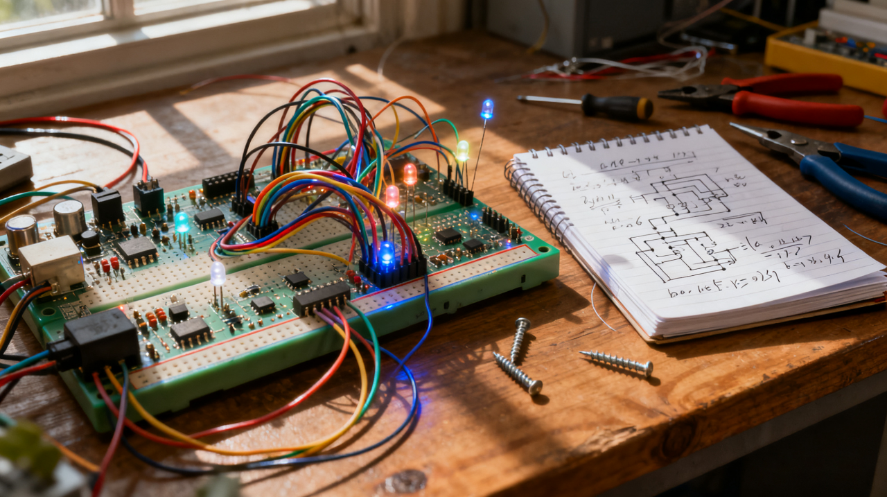
From Breadboard to PCB Printed Circuit Board: A Maker’s Journey
10/22/2025 at 08:14 • 0 commentsI once had a table full of wires, blinking LEDs, and tiny parts scattered everywhere. It was my breadboard—but honestly, it looked like chaos. Yet, in that mess, ideas came alive.
I wanted something better: a real, neat circuit I could build once and use forever. A circuit that didn’t fall apart if I touched it.
If you love making things with your hands, solving puzzles, and seeing your ideas take shape, this journey is for you.
In this article, I’ll take you step by step from a messy breadboard to a polished PCB printed circuit board. I’ll share my wins, my mistakes, and tricks to make your journey smoother.
![]()
Breadboard Prototyping
Before making a PCB, we start with a breadboard. A breadboard is a plastic board with lots of tiny holes where you can plug in wires and parts. It lets you test your ideas fast without soldering.
1. Why Use a Breadboard First?
- Quick Testing: You can try your circuit right away. Want to see if an LED lights up? Plug it in and check.
- Easy to Fix: If a wire is in the wrong place, you can move it in seconds. No soldering, no damage.
- Easy to Change: If you want to add a button, change a resistor, or try a new chip, it’s simple. Just plug it in.
Think of it like building with LEGO. You can make changes anytime without breaking anything.
2. Breadboard Wiring Tips
- Use Color-Coded Wires: Red for power, black for ground, other colors for signals. This helps you see what’s what at a glance.
- Plan Power and Ground: Keep a clear line for power (+) and ground (–). It prevents mistakes and makes your circuit stable.
- Small tip: Lay wires flat and short. Long, tangled wires make your breadboard messy and hard to debug.
3. Breadboard Debugging Experience
Even a simple breadboard can give trouble. Here are common problems and tips:
- Loose Connections: Parts may not sit fully in the holes. Push them gently but firmly.
- Wrong Wires: Double-check each connection. A single wrong wire can stop the whole circuit.
- Noise Issues: Long wires can pick up interference. Keep wires short, and separate power lines from signal lines.
- Measure voltages with a multimeter to see if the power reaches each part.
- Use an LED to test signals—it’s a simple “is it working?” light.
- For more complex circuits, a logic analyzer can help you see digital signals and find problems faster.
Quick Tricks:
Breadboarding is like the rehearsal before the big show. You test, fix, and learn before making the real PCB.
![]()
Schematic Design
Once your breadboard works, it’s time to draw the schematic. A schematic is like a map for your circuit. It shows how every part connects, so you can turn it into a PCB later.
1. From Breadboard to Schematic
- Record Every Connection: Look at your breadboard and note where each wire goes.
- Choose the Right Parts: Pick the exact resistors, capacitors, and chips you used.
- Think About Sizes: Make sure the parts you choose have a footprint that matches your future PCB.
Tip: Take a picture of your breadboard before unplugging anything. It helps a lot when drawing the schematic.
2. Using Free Tools
There are many free tools for making schematics:
- KiCad: Popular and powerful for serious makers.
- EasyEDA: Simple and online, good for beginners.
- Eagle: Widely used, has free version for small projects.
Tip: Most of these tools have libraries with common parts. Use them—they save a lot of time.
3. Schematic Design Tips
- Keep It Clean: Don’t crisscross wires too much. A clean schematic is easier to read and reduces mistakes.
- Add Labels: Name important signals like VCC, GND, or DATA. It helps later when making the PCB.
- Plan for Power and Ground: Show a clear path for power to every part.
- Think in Modules: Break your circuit into small blocks (like LED section, button section). It’s easier to debug and understand.
A good schematic is your blueprint. The better you draw it, the easier it will be...
Read more


 in advanced circuit designs")
")


 for electronics assembly, showcasing hands-on PCB assembly skills for electronics projects.")

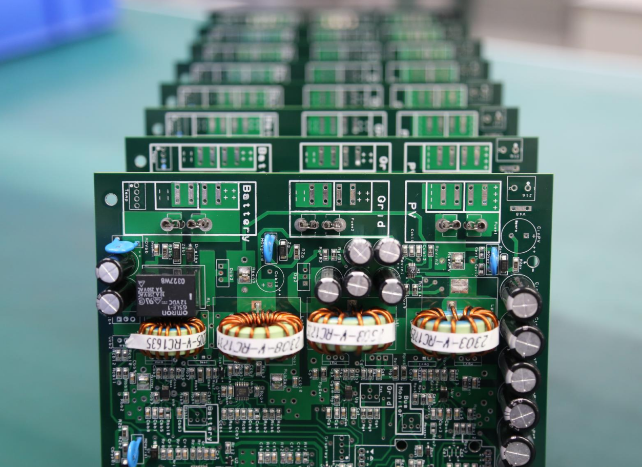


 showing layers, layout, and manufacturing process for electronics.")
 with components illustrating PCB structure, definition, and core function.")