 Samuel A. Falvo II
-
Rust Version of 'e' Emulator Coming Soon.
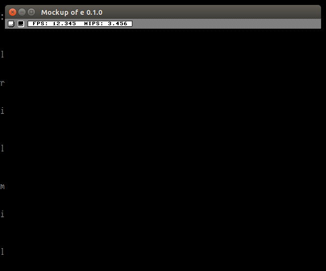
01/09/2017 at 07:03 • 0 commentsIn between hacking on the hardware, I've also been teaching myself the Rust programming language. I'm using this opportunity to try and fix some long-standing design issues with the original C-based code. One of those issues is the lack of a user interface that supports inserting and removing SD cards. I wrote some code to produce a quick mock-up of what I'd like to see. The top bar of the window contains icons which lets you insert or remove SD cards (the left icon represents an empty SD slot, while the right indicates an occupied SD slot), along with a simple performance status bar. The large black space, obviously, represents the 640x480 pixel output of the MGIA or CGIA core.
![]()
The user interface library is independent of the emulator project as a whole, but nonetheless written to support it. It's currently modelled after the Commodore 64/128 version of GEOS. Maybe as time progresses, I can evolve it to support more functionality from the GEM user interface.
-
Asynchronous CellularRAM integration failure.
01/07/2017 at 21:39 • 8 commentsI've been trying to get Micron's cellular RAM chip, as found on the Digilent Nexys-2 (MT45W8MW16 series chip) to function in its documented asynchronous RAM mode, to no success.
It supports reading from the chip with a great deal of ease; but, trying to get the chip to properly respond to memory writes has proven something of an impassible brick wall of a challenge for me.
I'm currently trying to adopt its synchronous mode of operation as I write this log entry. This has several deleterious effects to the Kestrel-3:
- The CPU now requires 3 clock cycles instead of two to access a single half-word of memory. This 50% increase in latency means video and CPU memory accesses can top out only at 8.3 mega-transfers per second. This is 16.6MBps throughput at best, since it's only a 16-bit wide path to memory. This is just enough to support 640x480 16-color displays, which rather sucks (I wanted a 256-color display), but at least it'll be in color.
- The CPU will top out best-case at only 4 MIPS. So, on average, you're going to more likely see 2 MIPS throughput. This is a 300% drop in anticipated performance, putting the computer squarely in the same performance bracket as an Atari 520ST (estimated), provided you use the same video resolutions (e.g., no higher than 640x200 in most cases).
I can reclaim the lost performance when I start to support caching in the CPU. This will allow me to use the PSRAM's "burst" mode, letting me amortize the access time to the chip across 4 or 8 consecutive half-words of memory. However, caches are expensive, complex, and extremely error-prone to implement. I want something, anything, running right now. I don't want to have to wait forever for a computer design that I have know knowledge if it'll work or not.
All in all, I'm not happy about this turn of events. I cannot fathom why the PSRAM chip is incapable of committing writes; I'm not violating any timing that I can see. Normally, you have to work extra hard to get RAM chips to not store spurious data! I am hoping beyond hope that adopting a synchronous memory controller will allow things to work better.
-
Discovering Memory Address Windows Without Device Trees
12/28/2016 at 22:27 • 1 commentA new long-form blog article has been posted on my official blog.
Abstract
Device trees are used to communicate existence of non-discoverable hardware, such as where scratchpad memory appears in the processor’s address space, to an operating system. Newer platforms, such as RISC-V, offer the opportunity to design systems in a way that obviates the need for complexities such as device trees; yet, these opportunities are often not exploited. The Kestrel-3 is designed to minimize its need for any kind of device tree-like concept through, in part, common sense rules concerning address decoding and sensible system software. This allows the system firmware and/or operating system to discover the hardware’s boot-up RAM address decode window with an algorithm substantially simpler than a typical device tree parser.
-
KCP53000 CPU Is Now FPGA Proven!
12/21/2016 at 03:37 • 1 commentI'm happy to report that I got the KCP53000 CPU and GPIA combination to actually blink an LED on the Nexys-2 FPGA development board!
The CPU is clocked at 25MHz; when executing the following sequence of instructions:
ledblnk:        srli    x3, x1, 24    ; 5 cycles
                sh      x3, 2(x2)     ; 5 cycles
                addi    x1, x1, 1     ; 5 cycles
                jal     x0, ledblnk   ; 5 cycles
in a loop 16,777,216 times, wall-clock measurements seems to suggest that the CPU is executing 4.8 MIPS. After adding up anticipated cycle counts for each of these instructions, I discovered (by doing the math in reverse) that the CPU should have been clocked at 23.9MHz (and some change). This represents an error of 4.4%; so, I'm going to say that the actual performance is probably closer to 5.0 MIPS in reality. Until I can get a console working, and actually read out the mtime and minstret CSRs, I can't be sure.
The KCP53000 talks to a KCP53001 arbiter to unify the two Furcula buses into a single memory bus, which then feeds into a KCP53003 64-bit-to-16-bit Furcula bridge, and then into a KCP53002 Wishbone bridge. From there, we access Kestrel-2 peripherals GPIA and an inferred ROM (presumably using block RAM resources).
It is regrettable that CPU performance will be cut in half when I access external RAM, due to its 70ns access time. However, this was to be expected; refining the CPU so that it overlaps instruction fetch and execution will go a long way towards recovering that lost performance later on. But, first, I need to focus on getting a functioning computer design. This is a big first step in that direction.
-
64-bit to 16-bit Furcula Bridge ("Bottleneck") Completed
12/14/2016 at 02:29 • 0 commentsI recently completed the first implementation of the circuit that will enable me to deploy my CPU on a real FPGA: the 64-bit to 16-bit Furcula bus bridge. This bridge supports not only 8- and 16-bit transfers, but also includes a state machine to support 32- and 64-bit transfers as well. NOTE:Datasheets for this component does not yet exist, but I'm hoping the circuit interface is easy enough to figure out by looking at the Verilog module header. I will provide documentation at a later date.
This bridge allows the host CPU, which relies on a 64-bit architecture, to interoperate with a 16-bit path to memory, which is what most FPGA developer boards offer.
-
Patreon Page Now Available!
12/07/2016 at 20:32 • 0 commentsSince I'm currently unemployed, and would actually prefer to be working on Kestrel full-time, I've decided to put up a Patreon page for the project in the hopes that some day, I can rely on fans of the Kestrel Computer Project for sustenance in exchange for more Kestrel development. A link is available both my main website as well.
Many thanks if you think the project is worthy enough to warrant a contribution, or even if you gave it a thought and decided against it. Either way, I hope to be able to deliver more Kestrel developments in the future.
-
Severe Down-Spec on Kestrel-3
12/02/2016 at 17:53 • 11 commentsAfter researching the different kinds of memories one has available to them on different FPGA boards, in conjunction with how utterly difficult it is to actually use some of these memories, I've decided to remove the 8MB of RAM specification for the Kestrel-3. Instead, I'm now going to set the RAM requirement to 256KB static RAM minimum.
This is a breaking change, and will require alteration to the software emulator, eForth, and the documentation. However, I cannot see any way around this change.
For main-line storage, virtually all FPGA boards I've looked at tends to offer either 1MB to 16MB of static(-like) RAM OR 16MB to 64MB of (sometimes DDR) SDRAM plus 512KB of static RAM. Since SDRAM represents clinical levels of insanity to initialize, to the point where hardware controllers literally just punt completely on the problem and modern CPUs must resort to such insanity as using cache RAM as scratch-pad RAM, I've decided it's best to specify a minimum amount of scratch-pad for use in bringing up the remainder of the system instead.
This means that eForth will have access to only 256KB of RAM minimum, not 16MB as it currently does in the emulator. Moreover, MGIA/CGIA's default frame buffer will be located in the 256KB block guaranteed to exist. This allows the system software to continue to display diagnostics as required. (Exception: for BlackIce boards, no video output will exist, and all I/O must occur through PMOD interfaces of some kind.)
Speaking of system firmware, the capacity for that will also need to drop as well, to something that will actually fit in the BlackIce project. However, I'll make a separate announcement on this later, once I have more data about what can and cannot fit. However, at least its location in the address space will remain where it's at.
This change should be trivially supported by most FPGA boards, since most offer 512KB to 1MB of static RAM of various speeds. Nexys-2 can be configured to offer up to 16MB, since its cellular RAM chip is of that capacity. However, to gain more capacity, most FPGA boards will need to run some software to train the SDRAM interface before using it. (Or, at least, have the benefit of a suitably intelligent hardware controller to do it for the system software.)
I'll be implementing these changes, probably about the same time as I switch the 53000 over to booting and running in user-mode instead of machine-mode, since that too is a breaking change. Might as well break everything all at once!
-
Datasheet Updated, Bugs Fixed
11/26/2016 at 16:53 • 0 commentsThe datasheet for the KCP53000 has been updated. A new Example chapter illustrates a typical application of the CPU. You should be able to simulate the Verilog inside of Icarus Verilog at the least. At least, "it works for me."
In addition, the example code includes a prototype of the (unlabelled) KCP53001 Furcula bus arbiter, which is used to convert the CPU's native Harvard architecture interface to a Von Neumann/Princeton architecture interface. It further includes a crude prototype of what will eventually become the KCP53002 Wishbone bus bridge/adapter as well. Together, the KCP53000, KCP53001, and KCP53002 forms a processor complex which can replace the S16X4 in the Kestrel-2. With some address space changes (which involve changing the emulator too), I should be able to realize a prototype of the Kestrel-3 in relatively short order. I still need to work on the Wishbone arbiter and the external SRAM interface.
I also discovered a surprise when trying to use the SLT and SLTU instructions. They always returned 0, even when the expected condition held true! This was due to some missing connectivity both within the ALU circuit and between the ALU and the execution state machine. This has been fixed.
If anyone is attending the 5th RISC-V Workshop, I will be giving a poster session there, and will have a hard-copy print-out of the datasheet for public review. Once again, I'll have my laptop computer available running the Kestrel-3 emulator, with eForth 1.0 running in (emulated) firmware.
I was hoping to have a simple game written that people can interact with, but alas, time is running much too short for me. Maybe next year, and maybe on a real FPGA system!
-
KCP53000 Runs Its First Program. Kind of.
11/13/2016 at 16:28 • 0 commentsI'm happy to report that, inside of a Verilog simulation, the KCP53000 has run its very first program. Kind of.
I'm being somewhat unfair though; see, the circuit consists of the CPU coupled to a simple ROM which is direct-wired onto the I-port of the processor, while the D-port is hard-wired to the value $41. So, when this program attempts to print its "Hello world" message, all it prints out is a bunch of "A"s. So, in that respect, the processor is doing exactly what it should be doing.
What's missing is a Wishbone bus bridge which I can use to couple the D-port to the same ROM image. Additionally, I'll be needing a Furcula bus arbiter to funnel both I- and D-ports into the same Wishbone interconnect. Once I have that, I can then perform address decode and mapping of ROM and RAM, and both should be equally accessible for instruction or data access.
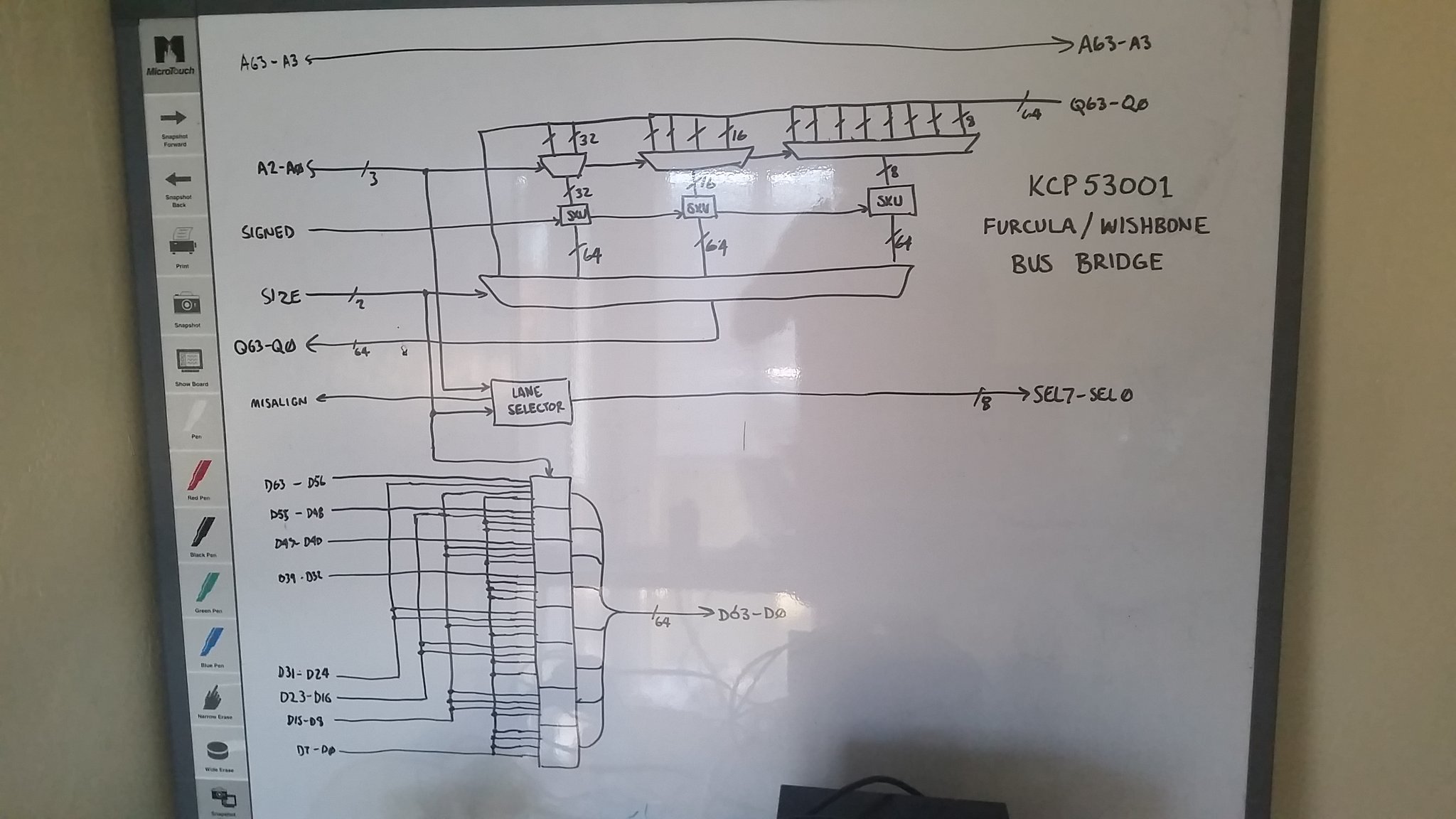
I've worked up a conceptual model of the Wishbone bus bridge.
![]() As you can see, it is largely an arrangement of multiplexors and zero/sign-extension units. The most complex part of the unit is going to be the byte lane generator, which is really a 32-minterm piece of logic that generates Wishbone's SEL_O signals as well as an error indicator back to the CPU, MISALIGNED (which I'll ignore for now, since CPU doesn't yet have such an input).
As you can see, it is largely an arrangement of multiplexors and zero/sign-extension units. The most complex part of the unit is going to be the byte lane generator, which is really a 32-minterm piece of logic that generates Wishbone's SEL_O signals as well as an error indicator back to the CPU, MISALIGNED (which I'll ignore for now, since CPU doesn't yet have such an input).I haven't quite figured out how to implement the bus arbiter just yet. Since I know that the KCP53000 cannot yet overlap its bus cycles, I might just logically-OR all the buses together and go with that for now. However, when I implement fetch/execute pipelining later on, that approach will fail spectacularly. However, with the SVFIG Forth Day and 5th RISC-V Workshop just around the corner, this stop-gap just might be worth the do-over later on.
-
External Interrupt Supported
11/05/2016 at 07:06 • 0 commentsThe KCP53000 Verilog code now supports an external interrupt input. Interrupts have priority over other kinds of traps; because the MEPC register always points to the instruction that faults (or that would have faulted), an MRET instruction returns to that instruction and, presumably, would fault again for the same reasons. Thus, faults are never lost.
Kestrel Computer Project
The Kestrel project is all about freedom of computing and the freedom of learning using a completely open hardware and software design.
 As you can see, it is largely an arrangement of multiplexors and zero/sign-extension units. The most complex part of the unit is going to be the byte lane generator, which is really a 32-minterm piece of logic that generates Wishbone's SEL_O signals as well as an error indicator back to the CPU, MISALIGNED (which I'll ignore for now, since CPU doesn't yet have such an input).