Jarrod
-
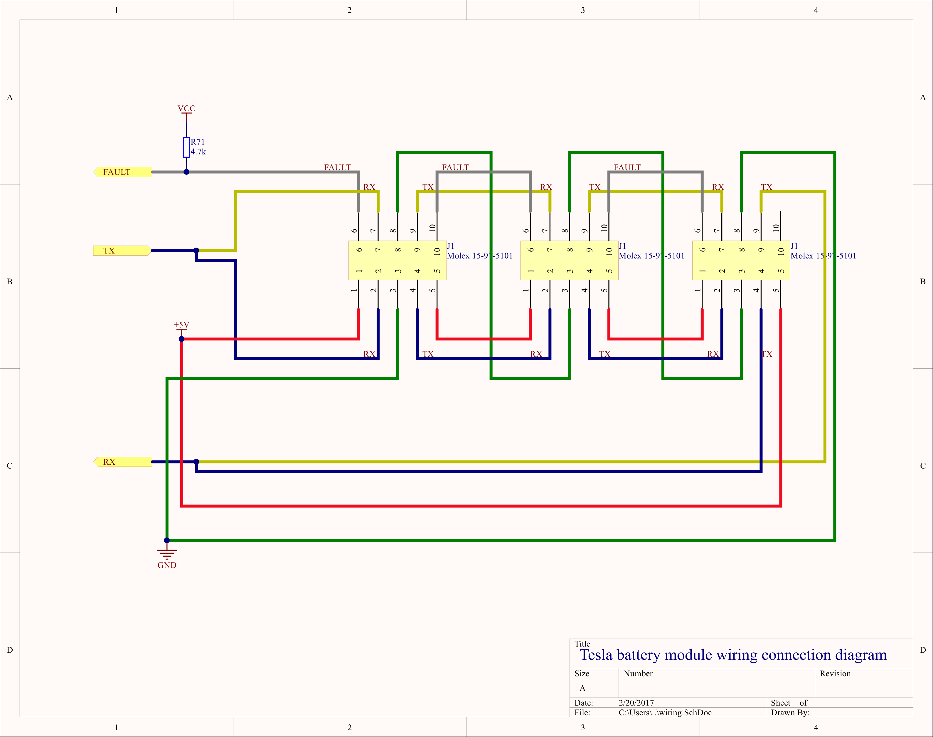
Wiring modules together
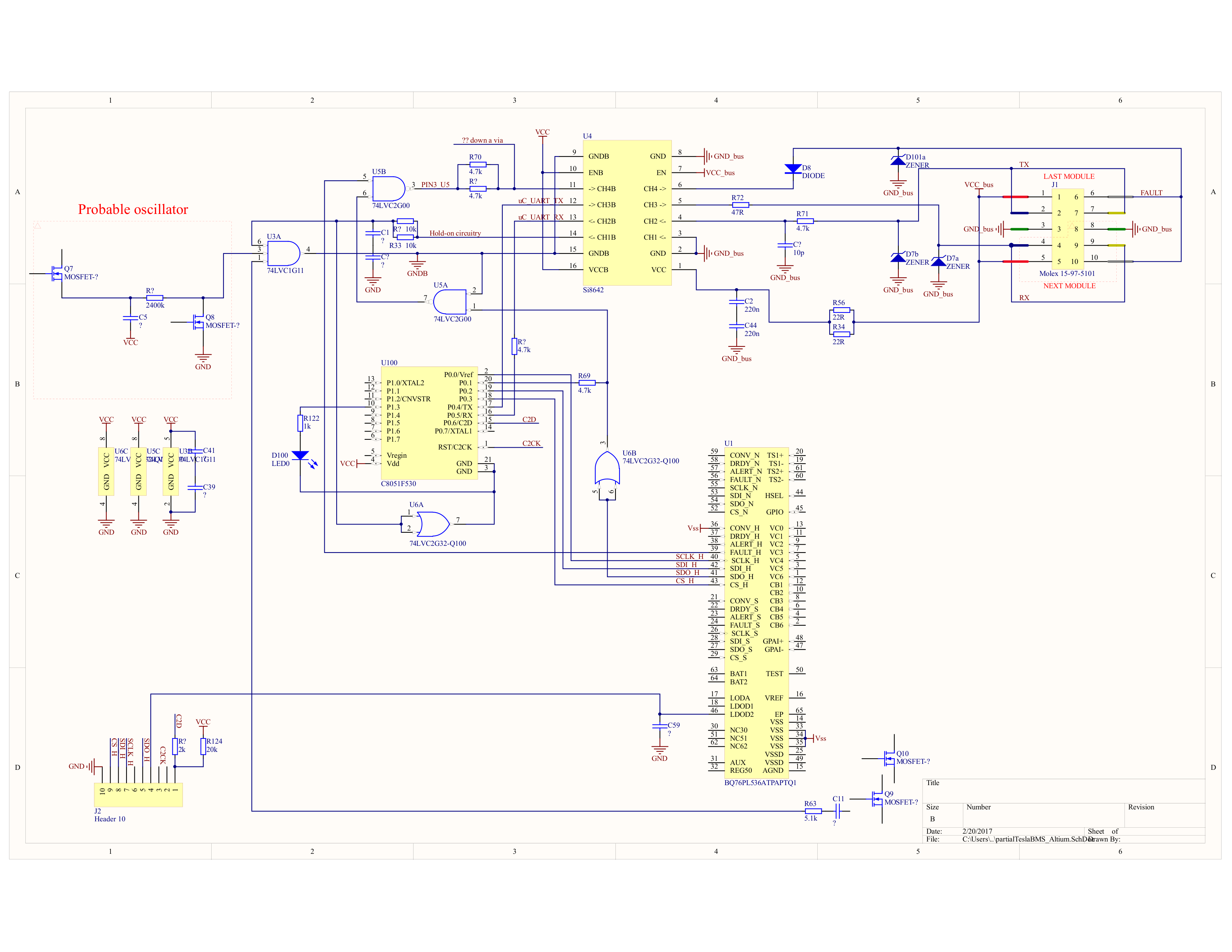
03/02/2017 at 05:30 • 1 commentI spent some more time tracing out the logic between the RF isolator and microcontroller to try and determine the actual function of the 4th channel on the isolator and just how the power down circuits work.
Ch4 does appear to be a fault line, it is connected, via a NAND gate to the FAULT_H pin on the BQ76 BMS IC, so this will drive the shared fault line (on pin 6 and 10 of the main connector) low in the case of an over temperature, over voltage or under voltage event. A diode is used to make it a dominant fault line, ie any fault on any module will force a fault state. This should work even if a module microcontroller stops responding (which would otherwise kill the daisychain UART communications.) Weirdly, the other pin of this NAND is derrived from a second NAND of the SDO pin and the RF com chip disable line. It's not clear to me what this achieves.
![]()
I also found the main connector (J1) part number by sorting through digikey, It looked like a Molex, that and the pins + spacing was enough to go on. Connector is Molex 15-97-5101, pins are 39-00-0038, retaining key is 15-97-9101.
So now it's pretty clear how the modules should be wired up to a controller. Here is an example for three modules (it can be extended to any number, up to 62 from what I can tell)
![]()
![]()
All this wiring is isolated from the cells, so the gnd and +5V can safely be on the 12V wiring potential in an automotive application.
A couple of the other team members, Collin and Tom are working on an Arduino sketch to interface with the serial protocol based on my earlier findings, this should now be ready to test out and get basic functionallity like voltage and current readings. https://github.com/collin80/TeslaBMS
Or if you have python and an FTDI board and just want to mess around, try the python script in the files section of this hackaday.io project.
-
bms settings
02/16/2017 at 08:41 • 2 commentsOne of the reasons I wanted to reverse engineer rather than replace the microcontroller on the module BMS board is that Tesla have carefully selected voltage levels for under/over voltage thresholds and balancing levels. So it's a bit of a bummer to find that the modules themselves don't seem to have these values built in, it's handled higher up the control chain.
But the BQ76 does have a hardware over and under voltage threshold, as well as over temperature built in, which pulls a shared fault line low.
There are also some other configuration values worth reading out, and since I do have a bunch of boards which have had power applied since the last time they were used, since they have this huge battery backup - the hundreds of 18650 cells - to keep the RAM powered!
So how do we read it out? need to find the address first, using my python script we can iterate through the possible addresses with something like
for address in range(0x3E):
    sendData(Read,[address, 0x00, 0x4C])
And eventually, at address=0x0F I get the result:
TX: 0x1e, 0x0, 0x4c,
RX: 0x1e, 0x00, 0x4c, 0x81, 0x2a, 0x25, 0x25, 0xa5, 0x25, 0xab, 0x25, 0xae, 0x25, 0xad, 0x25, 0xac, 0x25, 0xaa, 0x0a, 0x99, 0x0a, 0x93, 0x00, 0x00, 0x00, 0x00, 0x00, 0x00, 0x00, 0x00, 0x00, 0x00, 0x00, 0x00, 0x00, 0x00, 0x00, 0x00, 0x00, 0x00, 0x00, 0x00, 0x00, 0x00, 0x00, 0x00, 0x00, 0x00, 0x00, 0x00, 0x00, 0x3d, 0x03, 0x00, 0x00, 0x00, 0x00, 0x00, 0x00, 0x00, 0x00, 0x00, 0x8f, 0x00, 0x00, 0x00, 0x00, 0x10, 0x80, 0x31, 0x81, 0x08, 0x81, 0x66, 0xff, 0x15, 0x00, 0x00, 0x00, 0xad,
Labeling each register:
0: 81        #status register
1: 2a 25     #GPAI measurement data
3: 25 a5     #cell 1 voltage data
5: 25 ab     #cell 2 voltage data
7: 25 ae     #cell 3 voltage data
9 25 ad      #cell 4 voltage data
b: 25 ac     #cell 5 voltage data
d: 25 aa     #cell 6 voltage data
f: a 99      #TS1 voltage data
11: a 93     #TS2 voltage data
13-1f rsvd
20: 0        #alert status
21: 0        #fault status
22: 0        #OV fault state
23: 0        #UV fault state
24: 0        #parity result A
25: 0        #parity result B
26-2f rsvd
30: 3d       #ADC measurement control
31: 3        #I/O pin control
32: 0        #cell balancing control
33: 0        #cell balancing max on time
34: 0        #ADC conversion start
35-39: rsvd
3a: 0        #group 3 registers write access control
3b: 8f       #Address register
3c: 0        #reset control
3d: 0        #test mode selection
3e: rsvd
3f: 0        #EPROM programming enable
40: 10       #Function configuration
41: 80       #IO configuration
42: 31       #OV setpoint
43: 81       #OV time delay
44: 8        #UV setpoint
45: 81       #UV time delay
46: 66       #over temperature set point
47: ff       #over temperature time delay
48: 15       #user data 1
49: 0        #user data 2
4a: 0        #user data 3
4b: 0        #user data 4
So the values after 0x3F are identical to those read from the EPROM on a restart, they set to OV/UV/OT and time delays.
OV setpoint = 0x31, datasheet says 2V + 50mV * 49 = 4.45V
UV setpoint = 0x08. datasheet says 0.7V + 100mV * 8 = 1.50V
OT setpoint = 0x66. Table 2 says this corresponds to 1.578V, which is 65C for a 10k NTC such as ERT-J1VG103FA
Interesting values, the cells will basically be on fire if they reach these voltages.. The temperature value is much more reasonable.
Since we can't guarantee the register content, best practice is to just reset the BQ76 chips with a broadcast reset, then set it up from scratch. EPROM values will be loaded automatically but there are a few registers that require setup after a reset, Address control, ADC control, IO control and the fault and alert registers.
### ~~ Startup Code ~~ ###
#A5 is the magic value to reset the chips
sendData( Write, [broadcast, RESET_CONTROL, 0xA5])
#set address
sendData( Write, [0x00, ADDRESS_CONTROL, address|0x80]) #do this for each BMS on the daisychain
#configure ADC
sendData( Write, [address, ADC_CONTROL, 0x3D])
#configure IO
sendData( Write, [address, IO_CONRTOL, 0x03])
#clear faults, need to write a 1 to the fault bit to be cleared, then a zero
sendData( Write, [address, ALERT_STATUS, 0x80])
sendData( Write, [address, ALERT_STATUS, 0x00])
sendData( Write, [address, FAULT_STATUS, 0x08])
sendData( Write, [address, FAULT_STATUS, 0x00])
I've put a new version of the python script in the files section which also reads out and converts the ADC values to voltages.
-
UART protocol cracked!
02/15/2017 at 03:44 • 7 commentsAs I found in the last post, the isolated UART bus daisychained through the Tesla modules is running at an odd frequency, 612,500bps. This is problematic as it is not a standard PC baud rate. I had an FTDI board lying around so I had a peek at the datasheet to discover it has a highly configurable baud rate generator, easily configured to within 3% of 612kbps. In addition, the windows driver handles configuration automatically.
To test this out I wrote a python script, PySerial was fine with the non standard rate, and the frequency was confirmed with a logic analyser.
One of my collaborators, Tom has been probing out a module BMS hooked up to a master board, he found that a serial string is periodically transmitted and this results in SPI bus activity, just the status register being read. However, we had issues decoding the exact UART messages as he was lacking decent analysis tools. I Figured I would try repeating the test by sending the supposed data with my FTDI board anyway.
![]()
All I observed was each byte being repeated on the other side of the daisychain bus as expected from analysing the UART ISR code. I started modifying the bytes and noticed any string starting with 0x00 or 0x01 was repeated with that first byte modified to 0x80 or 0x81. At first I thought it was a read error but it was consistant and verified with a logic analyser.. Still no activity on the SPI bus.
Then a coding mistake led me to send long strings of 0x000000 etc. running the logic analyser I saw the SPI bus come alive!
![]()
The UART responded with an additional 0x00. The SPI bus had repeated the 0x000000 message and added/read out a 0x00, It's like the microcontroller is acting as a UART/SPI bridge, with something funny happening on the first byte.
Working on this theory, I constructed a valid SPI read message according to the datasheet: http://www.ti.com/lit/ds/symlink/bq76pl536a-q1.pdf
![]()
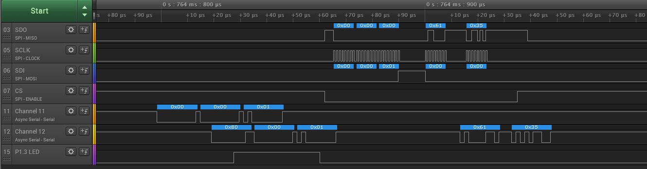
Lets try 0x00 00 01 - This should read 1 byte from device 0, address 0
And I got a reply! 0x61. 0x35 is the CRC8 of 0x00000135 This was the same reply recorded by Tom with his master/module BMS pair. strangely a very different uart command to what he seemed to record so there may be more to this. But it does seem like the microcontroller provides (almost) direct SPI access.![]()
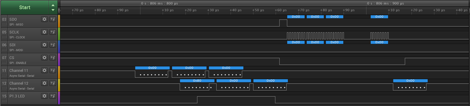
Taking it to the extreme, lets read out all the registers by sending 0x00 0x00 0x4C as there are 76=0x4C total register bytes
RX: 0x80, 0x00, 0x4C, 0x61, 0x00, 0x00, 0x00, 0x00, 0x00, 0x00, 0x00, 0x00, 0x00, 0x00, 0x00, 0x00, 0x00, 0x00, 0x00, 0x00, 0x00, 0x00, 0x00, 0x00, 0x00, 0x00, 0x00, 0x00, 0x00, 0x00, 0x00, 0x00, 0x00, 0x00, 0x00, 0x80, 0x08, 0x00, 0x00, 0x00, 0x00, 0x00, 0x00, 0x00, 0x00, 0x00, 0x00, 0x00, 0x00, 0x00, 0x00, 0x00, 0x00, 0x00, 0x00, 0x00, 0x00, 0x00, 0x00, 0x00, 0x00, 0x00, 0x00, 0x00, 0x00, 0x00, 0x00, 0x10, 0x80, 0x31, 0x81, 0x08, 0x81, 0x66, 0xff, 0x15, 0x00, 0x00, 0x00, 0x7F
SWEET!
Side note, looks like there is EEPROM data being loaded in for the UV/OV points and timers too. Translates to overvolt threshold of 4.45V and undervolt threshold of 1.5V, which seems very low to me.. I'm guessing the master BMS handles much of the protection by polling the cells. The GPAI ADC channel is also pointed to VBAT, so this channel is by default going to be measuring the voltage of all 6 cells in the module.
So taking a closer look at the first byte as this clearly differs from the SPI protocol and contains some undocumented magic. It's my best guess that bit 7 is used as a blocking bit to allow address assignment to each module. The middle 6 are the device address as per datasheet. So the last bit must be the R/W bit. (which is why both 0x00 and 0x01 have the bit7 blocking bit set when they are repeated)
I confirmed this by writing to the address register, then reading it back using the new address:
TX: 0x01, 0x3b, 0x81, 0x8b,
RX: 0x81, 0x3b, 0x81, 0x8b,
TX: 0x02, 0x3b, 0x01,
RX: 0x02, 0x3b, 0x01, 0x81, 0xba,
We write 0x81 to the address control register (0x3B), (where bit7 here indicates the address has been set, this clears an alert signal) so the new address is 0x01. to use the address, we must shift it left by 1, to get 0x02 as bit0 is the RW bit. The module now responds to the new address! In addition it no longer sets the 'blocking bit' - the leading byte is 0x02.
So if we try sending a message now to 0x00, it will be forwarded by this first module without modification:
TX: 0x00, 0x00, 0x01,
RX: 0x00, 0x00, 0x01,
The second module in the daisychain will then act on the string, set the blocking bit, and any other modules in the daisychain will thus ignore it, simply forwarding it on until it gets back to the master board (or in my case the FTDI serial interface)
Some other things I noticed, the on board microcontroller actually checks the CRC checksums for any write packets, it won't forward them over the SPI bus if they are wrong, this means we can't disable CRCs for SPI writes/replies on the BQ76 chip. The uC is clearly also recording the device address so it can handle the daisychain protocol and ignore packets not addressed to it. Broadcast packets are also supported (device address 0x3F)
So now anyone with an FTDI board (many other USB Serial interfaces may work too) communicate with a string of 1 to technically 63 tesla modules.
I've uploaded a Python script which sets the address of one module, then initiates an ADC conversion and reads out the result. I'll add more functionality and comments shortly, it can be found here:
https://cdn.hackaday.io/files/10098432032832/TeslaBMS.py
Or TeslaBMS.py in the files section of this project.
Next up: Designing an embedded BMS master board with a CAN bus and contactor (big DC relay) drivers.
Addendum: If you have a battery module pulled from a Tesla pack, it will still have the address it was assigned when operating in the Tesla, so it won't respond at the 0x00 address. Either reset it's address with a broadcast command or simply unplug the battery cable from the board. It's also worth noting that there is quite possibly a lot of extra functionality built into the microcontroller, the extracted code is vastly more complex than it should be for the above functionality. The function of the grey wire in the wiring harness is also unknown. likely a fault signal from the BQ76 BMS IC.
-
Firmware hacking
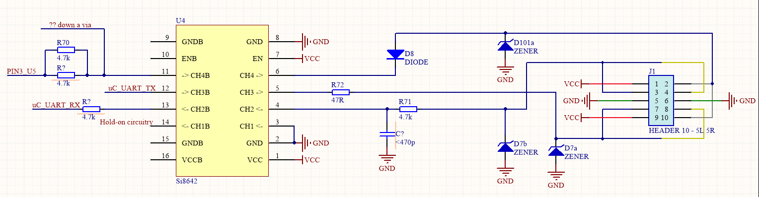
04/17/2016 at 20:22 • 2 commentsHere is a rough schematic of the isolated bus circuitry.
![]()
It looks like there is some shared "open collector" style bus on CH4 of the isolator, with D8 and (I assume) a pullup on the BMS controller board. But so far I've only ever measured this line being low, thus disabling the entire bus. I haven't worked out what U5 is yet. probably a dual logic gate. Maybe it combines error signals out of the BMS IC..
Ch1 is used to bring the BMS out of low power mode. A low frequency oscillator powers up U4 periodically checking on the state of CH1. The whole thing then stays powered while CH1 is driven low (otherwise CH1 is high impedance if the bus side of the isolator is unpowered, the circuitry must detect this and shut down) I can't really be bothered tracing out much more of the circuit. the layer of varnish on everything and tracks disappearing into internal layers makes it a nightmare.
Ch2 and 3 look like the main comms lines, connected to the UART of the uC. J1 is set up such that Tx of one channel is connected to Rx of the next, so they daisy chain together. The first BMS in the chain must get a "go" command from a controller board.. so I just have to work out how to say "go" as discussed in my last post.
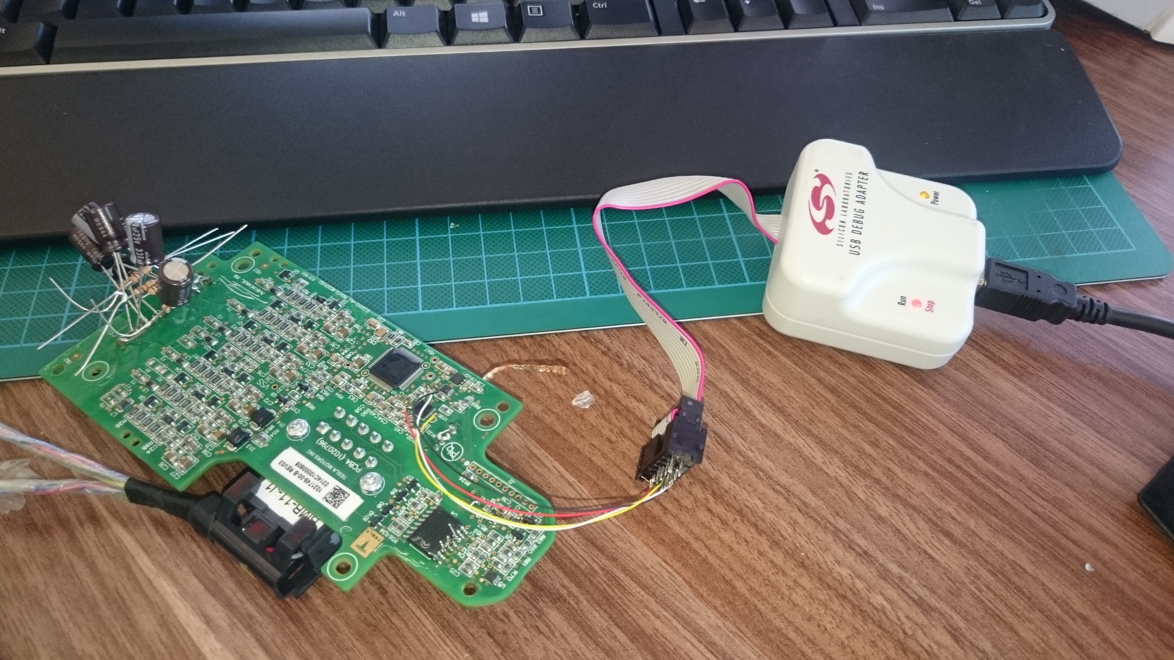
I thought I'd just check that Tesla had the security bit set to protect the firmware from reading.. already had a SiLabs JTAG/C2 programmer so I wired up the 2-wire C2 interface.
![]() And turns out.. The firmware is totally readable! Tesla wanted to make my life a bit easier. Thanks Tesla! There is about 5KB of used codespace. I ran it through an 8051 disassembler, DASMx. The SiLabs C51 uC's are totally 8051 compatible, meaning binary operands and memory locations are the same, so DASMx can even decode the SFR addresses into memonics for me. Its supposed to be able to 'flatten' out the code, using all the calls and branches to make it more linear to read but it would only process 3% of the code when I tried that option.
And turns out.. The firmware is totally readable! Tesla wanted to make my life a bit easier. Thanks Tesla! There is about 5KB of used codespace. I ran it through an 8051 disassembler, DASMx. The SiLabs C51 uC's are totally 8051 compatible, meaning binary operands and memory locations are the same, so DASMx can even decode the SFR addresses into memonics for me. Its supposed to be able to 'flatten' out the code, using all the calls and branches to make it more linear to read but it would only process 3% of the code when I tried that option.Here is the hex: https://cdn.hackaday.io/files/10098432032832/code.hex
And disassembled code: https://cdn.hackaday.io/files/10098432032832/code.lst
And the chip datasheet: https://www.silabs.com/Support Documents/TechnicalDocs/C8051F52x-F53x.pdf
There are a few thousand lines of assembly. I started by looking at the interrupts, as some of the code is most likely interrupt driven, especially the UART RX.
Code at 0x12A9: mov iec,#0B0H, this writes to the interrupt enable Special Function Register, enabling interrupts on Timer2 and UART0. The UART interrupt vector is 0x0023, which contains ljmp L0C0F, which does another ljmp L0DB9 which contains the code below!
0DB9                        L0DB9:
0DB9 : C0 E0        "  "        push    acc
0DBB : C0 F0        "  "        push    b
0DBD : C0 83        "  "        push    dph
0DBF : C0 82        "  "        push    dpl
0DC1 : C0 D0        "  "        push    psw
0DC3 : 75 D0 00    "u  "        mov    psw,#000H
0DC6 : C0 00        "  "        push    X0000
0DC8 : C0 01        "  "        push    X0001
0DCA : C0 02        "  "        push    X0002
0DCC : C0 03        "  "        push    X0003
0DCE : C0 04        "  "        push    X0004
0DD0 : C0 05        "  "        push    X0005
0DD2 : C0 06        "  "        push    X0006
0DD4 : C0 07        "  "        push    X0007
0DD6 : 30 99 05    "0  "        jnb    ti,L0DDE
0DD9 : 75 2B 00    "u+ "        mov    X002B,#000H
0DDC : C2 99        "  "        clr    ti
0DDE                        L0DDE:
0DDE : 30 98 30    "0 0"        jnb    ri,L0E11
0DE1 : 85 99 2A    "  *"        mov    X002A,sbuf
0DE4 : E5 2C        " ,"        mov    a,X002C
0DE6 : 60 21        "`!"        jz    L0E09
0DE8 : E5 2B        " +"        mov    a,X002B
0DEA : 60 05        "` "        jz    L0DF1
0DEC                        L0DEC:
0DEC : 30 99 FD    "0  "        jnb    ti,L0DEC
0DEF : C2 99        "  "        clr    ti
0DF1                        L0DF1:
0DF1 : E5 2D        " -"        mov    a,X002D
0DF3 : 60 0D        "` "        jz    L0E02
0DF5 : E5 2A        " *"        mov    a,X002A
0DF7 : 54 FE        "T "        anl    a,#0FEH
0DF9 : 70 07        "p "        jnz    L0E02
0DFB : E5 2A        " *"        mov    a,X002A
0DFD : 44 80        "D "        orl    a,#080H
0DFF : FF        " "            mov    r7,a
0E00 : 80 02        "  "        sjmp    L0E04
                ;
0E02                        L0E02:
0E02 : AF 2A        " *"        mov    r7,X002A
0E04                        L0E04:
0E04 : 8F 99        "  "        mov    sbuf,r7
0E06 : 75 2B 01    "u+ "        mov    X002B,#001H
0E09                        L0E09:
0E09 : 75 29 01    "u) "        mov    X0029,#001H
0E0C : C2 98        "  "        clr    ri
0E0E : 12 12 95    "   "        lcall    L1295
0E11                        L0E11:
0E11 : D0 07        "  "        pop    X0007
0E13 : D0 06        "  "        pop    X0006
0E15 : D0 05        "  "        pop    X0005
0E17 : D0 04        "  "        pop    X0004
0E19 : D0 03        "  "        pop    X0003
0E1B : D0 02        "  "        pop    X0002
0E1D : D0 01        "  "        pop    X0001
0E1F : D0 00        "  "        pop    X0000
0E21 : D0 D0        "  "        pop    psw
0E23 : D0 82        "  "        pop    dpl
0E25 : D0 83        "  "        pop    dph
0E27 : D0 F0        "  "        pop    b
0E29 : D0 E0        "  "        pop    acc
0E2B : 32           "2"         reti
This is clearly an interrupt service routine, you can tell by the push operations at the start (to back up working registers) and the pulls at the end, finished by a "reti" - return from interrupt operand.My analysis in comments:
	jnb	ti,L0DDE 		; branch if interrupt not caused by UART sending a byte.
	mov	X002B,#000H 	        ; clear 0x2B if byte had been sent already (0x2B is a 'byte sent flag' from later in this interrupt)
	clr	ti			; clear Tx interrupt flag
L0DDE:
	jnb	ri,L0E11		; branch if interrupt not caused by UART recieving a byte. exits interrupt
	mov	X002A,sbuf		; copy serial buffer to 0x2A
	mov	a,X002C			; 0x2C set outside of interrupt.
	jz	L0E09			; jump if zero
	mov	a,X002B
	jz	L0DF1			;jump if Tx interrupt flag was set above, this means we were interrupted by both rx and tx.
L0DEC:
	jnb	ti,L0DEC		; wait for Tx complete. as we sent a byte last time.
	clr	ti			; clear Tx interrupt flag
L0DF1:
	mov	a,X002D			; set elsewhere
	jz	L0E02
	mov	a,X002A			; move serial buffer to ACC
	anl	a,#0FEH			; bitwise AND
	jnz	L0E02			; branch if zero
	mov	a,X002A			; move serial buffer to ACC
	orl	a,#080H			; bitwise OR - set bit 7
	mov	r7,a			; move serial byte with bit7=1 to R7
	sjmp	L0E04
L0E02:
	mov	r7,X002A		; move serial byte to R7, either with bit0 cleared or not (if 0x2D == 0)
L0E04:
	mov	sbuf,r7			; write R7 back to serial buffer for transmission..
	mov	X002B,#001H		; this makes the interrupt wait for transmission next time it runs, the 'byte sent flag'
L0E09:
	mov	X0029,#001H		; set 0x29
	clr	ri			; clear Rx interrupt flag
	lcall	L1295		        ; this call clears ram 0x0023, 24, 25, 26
L0E11:
So basically it will receive a byte, save it to 0x2A then send it onwards IF 0x2C is nonzero. This supports the daisy chain hypothesis as it would appear (when enabled) the interrupt forwards packets. it also modifies bit7 of the packet under some circumstances, if 0x2D is set AND sbuf bit1-bit7 are zero (bit0 is ignored by the &0xFE) then it will set bit7. This would lead to a behaviour where the first device to get such a packet would modify it, the rest would simply forward it. Definately part of the daisy-chain control method. I'd imagine the packet would remain unmodified when a node is done transmitting. There is probably a 'Reset' packet to get the node transmitting again. bit0 is probably used for this as it remains unchecked and unmodified when forwarding packets.There is definitely some logic elsewhere in the program, time to search for code that looks at RAM 0x2A and sets 0x2D. Given the nature of compiled C code this is a ridiculous task, there are branches and calls everywhere. I think an 8051 emulator might be the way to go here.
###########--CBF--###########
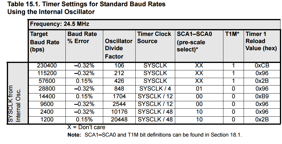
Another option is to try out sending packets like 0x00 and 0x01, see if anything happens. Need to know the baud rate for this. So, diving back into the datasheet, Timer1 is used to generate the UART clock:
UartBaudRate = 1/2 x T1_Overflow_Rate
T1_Overflow_Rate = T1CLK / ( 256 - TH1 )
Sysclk is configured with mov X00B2,#0C7H, internal oscillator enabled, SYSCLK derived from Internal Oscillator divided by 1, ie 24.5MHz
T1mode is set with mov tmod,#020H, Mode 2: 8-bit counter/timer with auto-reload as recommended for UART usage.
T1clk is configured with mov X008E,#018H to use sysclk with no divider
![]() TH1 is set by mov th1,#0ECH.. Which is not in the table. WTF. Non standard baud rate? ok then.. ( 24500000 / ( 256 - 236 ) ) / 2 = 612,500 bps.
TH1 is set by mov th1,#0ECH.. Which is not in the table. WTF. Non standard baud rate? ok then.. ( 24500000 / ( 256 - 236 ) ) / 2 = 612,500 bps. I guess the best way to test this out is another Silabs uC. I'll probably try that in the next log.
-
first steps
03/28/2016 at 20:12 • 0 commentsDid some probing of the BMS and tracing out of the isolated circuitry, I think I have figured out how the basic communication bus SHOULD work..
Looks like Tesla have powered down the uC and isolator chips to save energy when the car is turned off, they do this with a switch between the IC Vss/gnd and the TI BMS IC's Vss/gnd, looks like U5 and U5 are the switches. U2 appears to be a voltage regulator (judging by the heat it produces when powered on.)
They have an oscillator which enables the isolator IC periodically, if the bus side of the isolator is powered, pin 14 will be pulled low, this then enables the uC and isolator until the isolated bus is unpowered and pin 14 goes high impedance. When it poweres up, the uC flashes the onboard LED, but it doesn't send out any data, in fact it pulls the data line low..
Pin 17 of the uC is connected to an output channel of the isolator, pin 16 is connected to an input, these are UART TX/RX pins so it's a safe bet that some serial protocol is used to enable the board and read out data. and it's not just a simple
Unfortunately it's going to take a long time to brute force the serial baudrate and combination of bytes which makes data flow.. so this is a dead end unless I can get my hands on a working Tesla with it's pack ripped open to probe the bus.. Anyone?
Otherwise plan B is to write my own code to run on the Silabs uC and interface with the BMS IC.
Model S BMS hacking
Reverse engineer, reprogram or otherwise use the UV/OV/balancing circuits built into each of the 16 modules in a Tesla Model S battery pack.