Close
0%
0%

sdramThingZero - 133MS/s 32-bit Logic Analyzer

Add an old SDRAM DIMM to your SBC for a 133MS/s 32-bit Logic Analyzer, add ADCs for a Scope...

Similar projects worth following
Yes, it likely seems a bit ridiculous to add an old SDRAM DIMM to today's single-board computers with their whopping e.g. 512MB of onboard DDR2, but believe it or not THERE'S GOOD REASON!!!

Turn your SBC into a logic analyzer, data-logger, or an oscilloscope... You'll see! Read the Details!

This is a re-envisioning of its "father", sdramThing4.5:
https://hackaday.io/project/4159-sdramthing45-logic-analyzer

This new revision is more of a peripheral (rather than a complete system) which can be attached to microcontrollers, single-board computers, or even a PC's parallel-port.

The UI, datalogger, etc. can then be programmed in any language available on the host.

Turn your Raspberry Pi (or nearly any Single-board or even regular computer) into a 133MS/s 32-bit Logic Analyzer, or a 3-channel 10-bit 'scope, etc.!

-----------

This project and its "father" were blogged at Hackaday!

http://hackaday.com/2016/03/15/sdram-logic-analyzer-uses-an-avr-and-a-dirty-trick/

(Thanks Al Williams!)

http://hackaday.com/2016/07/19/hackaday-prize-entry-the-cheapest-logic-analyzer/#comment-3094325

(Thanks Brian Benchoff!)

And, was chosen as a finalist for The Prize!

(Thank you, judges!)

------------

Here's how I see it:

Add this ten-gallon "hat" to your PiZero, load a piece of software, possibly supply your own old SDRAM DIMM, wire it up to your 3.3V logic-to-be-analyzed, and you're ret-to-go.

(WHAT?! You're sticking an SDRAM DIMM on a single-board computer with already more/faster memory than that?! Why???)

----------------------

So, here's the deal...

(I'll use the Raspberry Pi as an example of the sorts of device this is intended to work with)

The Raspberry Pi is, essentially, a single-board computer. Its end-goal isn't interfacing to hardware at the bit-level, as much as it is to be a tiny full-fledged workstation...

This is different than, say, the BeagleBone, which (as I understand) is designed for high-speed interfacing with the outside world (For a great example of what it's capable, see @Kumar, Abhishek's #BeagleLogic. If you're looking to build an embedded-logic-analyzer, that's probably a better way to go!)

So, it's taken a few great minds*, here at Hackaday.io, to bring me to the conclusion that sampling data straight from most (but not all) Single-board-computers' GPIOs into their internal RAM causes a bit of a bottleneck.

* (Thanks especially to @usedbytes and @Vikas V over at #Operation: Try to Bare-Metal the Pi and #Logic analyzer using raspberry pi)

Enter External Memory...

By adding a bit of memory between the "real world" (logic analyzer inputs, ADCs, etc.), it's possible to sample data *really quickly,* then read that data into the RPi at whatever rate possible. Then, after it's read-in, it can be displayed, manipulated, zoomed, etc.

This isn't unlike most logic-analyzer peripherals.

Enter SDRAM:

SDRAM is, as far as I'm concerned, the last of the "easy-ish" memories to interface-with... It runs at 3.3V, doesn't require complex timing schemes (and huge sensitivity to skew) to handle data on each edge, etc... (At another level, it allows bursts longer than 8 data-locations, allows for somewhat-arbitrary clock-halting, and more).

Besides all that, it's pretty easy to find SDRAM DIMMs unused in piles... Why limit yourself to a single 16-bit-wide 16MB chip, when you can easily have 32 parallel bits and 64MB already wired-up for 133MHz speeds?

Enter sdramThing:

sdramThing is a (series of) project(s) I've been working on for several years. The latest version, prior to this, acts as a 30MS/s 32-bit "Logic Analyzer", of sorts, when connected to an AVR and an Oscilloscope.

The basic idea of all versions of sdramThing is to connect the SDRAM's "command"/address pins directly back to its data pins... Thus, by filling data-locations with specific instructions to be fed-back to the SDRAM, the SDRAM itself can "Free-Run" at the highest-speed its capable (133MHz, soon?), independent of a controller. It's definitely a loop, and definitely a "loopy" explanation. :)

Check out: #sdramThing4.5 "Logic Analyzer" and the home-page (

a bit outdated) at: https://sites.google.com/site/geekattempts/home-1/sdramthing for detailed explanations of how this "Free-Running" is possible.

Note that "Free-Running" uses one of the two "banks" of memory on a DIMM to store/repeat the commands. This bank, and thus half the available memory, can't be used for sampling data (however, it can be used for *outputting* data, arbitrary-waveforms, etc.). It may seem a bit wasteful, in a logic-analyzer-sense, but consider the alternative is a dedicated controller with 20+ GPIOs capable of precision timing at these speeds (which we've already determined the Gigahertz+...

Read more »

Spdsd12b.pdf

Intel's PC SDRAM Serial Presence Detect (SPD) Specification Rev 1.2B - Describes the information contained in the SDRAM DIMMs' EEPROMS. This *can* be useful, but again, don't trust that the data read is *entirely* accurate, as some manufacturers cut corners.

Adobe Portable Document Format - 141.08 kB - 08/05/2016 at 09:40

Preview

64mb_x4x8x16_sdram.pdf

Micron SDRAM chip Datasheet: MT48LC8M8A2 pretty much general-purpose for most SDRAM chips.

Adobe Portable Document Format - 5.99 MB - 07/23/2016 at 21:55

Preview

unb_001 SDR.pdf

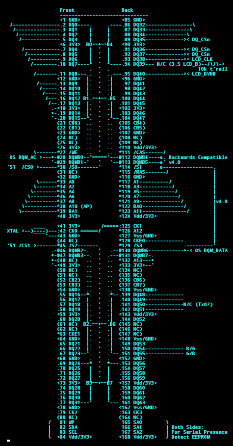
Intel’s PC SDRAM UNBUFFERED DIMM SPECIFICATION Rev 1.0 Pinouts, etc for DIMMs (Be sure to look at section 5. Also browse my gallery for a pinout I drew-up) BEWARE: NOT ALL DIMM-MANUFACTURERS FOLLOW THIS SPEC!

Adobe Portable Document Format - 438.95 kB - 07/23/2016 at 21:51

Preview

  • 1 × PC-133 SDRAM DIMM Most will work
  • 1 × 74AHC574 Electronic Components / Misc. Electronic Components
  • 2 × 74HC00 Electronic Components / Misc. Electronic Components
  • 1 × 30MHz Crystal Oscillator
  • 1 × Solderless Breadboard

View all 9 components

  • sdRamblingThing Concepts, revisited

    Eric Hertz04/15/2022 at 19:46 0 comments

    I've been contacted, recently, about someone's interest in trying this out... Specifically, if I understand, trying to create a state-machine with lookup-tables.

    I think it important to note HOW this thing [supposedly] works:

    Unlike typical Static or Dynamic RAMs, which you just supply an address and it gives the value at that address, SDRAM has a function called Read-Burst (also write-burst).

    When you start a read burst at some address, it outputs the data from that address, then automatically outputs the data from the address after that one during the next clock cycle, and so-on for a selectable number of addresses. E.G a typical burst-length setting is 4 or 8 locations.

    All the SDRAM chips I've worked with can be configured to burst an entire row of data (usually 256, 512, or 1024 bytes). 

    But, of course, a 1MB chip has way more than 1024 bytes... So a single read-burst /cannot/ output the entire chip's contents. 

    To do that, you'd have to start a new read-burst in the next row immediately after the first burst completes. (actually, due to CAS-Latency, it has to be started a few clock cycles *before* the previous burst completes, if you want an uninterrupted burst of two rows, or i.e. 2048 bytes).

    So, what I've done is add a second identical SDRAM chip in the mix (This is easy when using a DIMM!). This second chip is addressed with the same address bits, uses [most of] the same command-inputs. When a read-burst is initiated on the original chip, that same read burst occurs in this new/second chip. So, now, the two chips together burst 2 bytes simultaneously.

    Now, there's no reason to limit this to two chips. A DIMM actually has 8 chips or 8 bytes' worth of chips... So, I group them into two groups, each 4bytes wide...

    The memory I want to burst-read (or write) is 4bytes, 32bits. This is the Sample-memory in sdramThingZero (and #sdramThing4.5 "Logic Analyzer") logic-analyzer.

    This can also be, say, a framebuffer to drive a LCD... or, basically anything one might want to output/input in a huge continuous burst.

    Again, that group of chips, alone, would only be able to burst a maximum of 1024 32bit words, before requiring a precisely-timed NEW read-burst command, telling it to begin a new burst from the next row.

    So the other group of chips, 4 bytes' worth/32bits, is loaded-up with that command. This group (I call the "FreeRunner") has its data outputs tied [mostly] directly back to both groups' command/address inputs. (The other group, the "memory" for sampling, or a framebuffer, I poorly named "The SideKick"). 

    So, Now, the FreeRunner and the SideKick BOTH burst the same addresses at the same time. The FreeRunner is MOSTLY filled with "NOP" commands, so mostly doesn't interfere with a row-burst. BUT a few addresses shy of the last address in the burst, it requests a new burst in the next row. Which begins a few clock cycles later, immediately after the first completes.

    That's a bit simplified, but should do for now.

    Fill the FreeRunner with commands such that the SideKick will burst its entire contents in a continuous stream, 32 bits from each address, once per clock cycle.

    Great for sampling data in a logic analyzer, great for refreshing an LCD, I dunno what-all.

    ....

    So, the FreeRunner basically does little else than cycle through all the addresses in the DIMM.

    Unfortunately, not much at all like an EPROM lookup table, more like a VGA card. Heh. 

    ...

    However, it /is/ a bit like a very limited CPU, The addresses' incrementing after each NOP is a bit like a program-counter.

    Now, it is possible to send different commands to the Sidekick and Freerunner. Each group of 4 bytes has a separate Chip-Select. So, e.g. in a logic-analyzer setup, the Freerunner is always burst-reading (outputting the commands stored in it) while the Sample Memory (SideKick) may be burst-writing (sampling data, storing it in memory) OR burst-reading (outputting the stored samples back to the host...

    Read more »

  • Why'd I Stop?

    Eric Hertz01/11/2022 at 17:18 0 comments

    This's been in my drafts since the turn of the year (It's now mid-April, and it's been snowing!?). I didn't finish this writing, there's a TON more could be said about how things like this have taken their toll on me. And, quite frankly, I'm a bit afraid to talk about this stuff, for COUNTLESS reasons. But... It happened, and things like it continue to happen. These things affect me every day, some near-decade later, and to lesser-noticed extents some decade prior. Facts are facts, I suppose. Whatever the heck it is, it seems I just can't wrap my head around it, nor really how to function in any reasonable capacity with it's presence in my life. It is what it is (what is it?!). I'm doing the best I can with what I understand.

    Here's the original draft. Actually, I've tried to write about this COUNTLESS times, and I bet there are years-old drafts about it all over my projects' logs. Heh. Here's the January 2022 attempt:

    ....

    This project, you may've noticed, went from ludicrous-speed to full-stop in basically one evening.

    I've tried to explain to countless folk countless times and countless ways...

    I haven't explained, here, because, frankly, it scared me. The event itself, and the implications. Still affect nearly all my projects to this day. Years later. Heck, frankly, it affects nearly every aspect of my life.

    ...

    Today I woke with an analogy in my head...

     Imagine the "Pinball Wizard". This guy got really good at pinball, so good that he gained an audience. During a competition he made a mistake... he knows he did. He slipped, missed that button... No one else saw it. The paddle did its thing as though he hadn't. At the time he really didn't think about it... But after the excitement died down, he remembered his fumble... That should've been the end of his game, early-on. Instead, he went on for many more rounds, ultimately winning. What's he supposed to think? Eventually he puts it out of his mind... continues playing when he has time... Until another competition... huge crowd gathered around... He fumbles, again, yet the paddle hits the ball expertly... right up through "The Impossible Loop" gaining a gazillion points, flashing lights, and so many dings nearly every remaining angel-second-class must've gotten their wings. The crowd's going wild, but there's no paddling to do as the ball travels the loop. He knows he missed that shot, has time to think, he starts flailing on the paddle buttons... If those paddles did what they were told, that crowd would've thought he was having a seizure. When the ball returns, he hits it once or twice, as usual, then intentionally starts missing shots, yet those paddles keep hitting it perfectly. Eventually he just stops even pushing the buttons, but the game keeps playing without him.

    Hey, this is the 70's, we're talking about, gaming AI is about as sophisticated as Pacman's ghosts... There's no way even the refridgerator-sized computers of the era could achieve the level of real-time physics calculation to keep that ball in play.

    So what's left?

    Remote controls and a video camera?

    Whatever the case, even "in the zone" he knows he missed those shots, especially the ones he intentionally missed.

    .

    sdramThingZero was at a point where I was coding... Really low-level, I wrote my code changes in "baby steps," thoroughly testing each along the way. Small change, recompile, upload to the AVR, test test test, repeat. There's no operating-system to get a virus on a chip like this, no WiFi for remote-control... I'm coding in C at the lowest level possible. I wasn't even using others' libraries aside from defaults like avr-libc... heck, not even stdio. Certainly not Arduino. Basically aside from the initial boot code that calls main() I'd written /every/ piece of code running on that AVR. Heck, I wasn't even using a bootloader! My hex file was flashed at address 0.

    Unlike pinball, there was no reliance on timing with external factors... My process was lock-stepped....

    Read more »

  • TODOs

    Eric Hertz02/19/2019 at 03:16 0 comments

    Yup, sTZero's been on hiatus for a while... life 'n such.

    UPDATESs will be placed at the bottom...

    Here's a thought:

    SN74LVC1G123 - might just handle our one-shots... Personally, the idea of using RC timing doesn't quite sit with me, for this project, being largely variable in its sample-rate... But, maybe som'n can be done tying those R and C inputs to something like the SDRAM clock. Or maybe some other path, even with R and C fixed (e.g. at 10ns, for max-sampling at 100MS/s) as long as we can assure that 10ns pulse meets setup/hold times for the instruction-load clock-edge (when sampling at lower rates).

    Dunno...

    Anyhow: 

    https://hackaday.com/2019/02/18/inefficient-neopixel-control-solved-with-hardware-hackery/

    ----

    2-29-20:

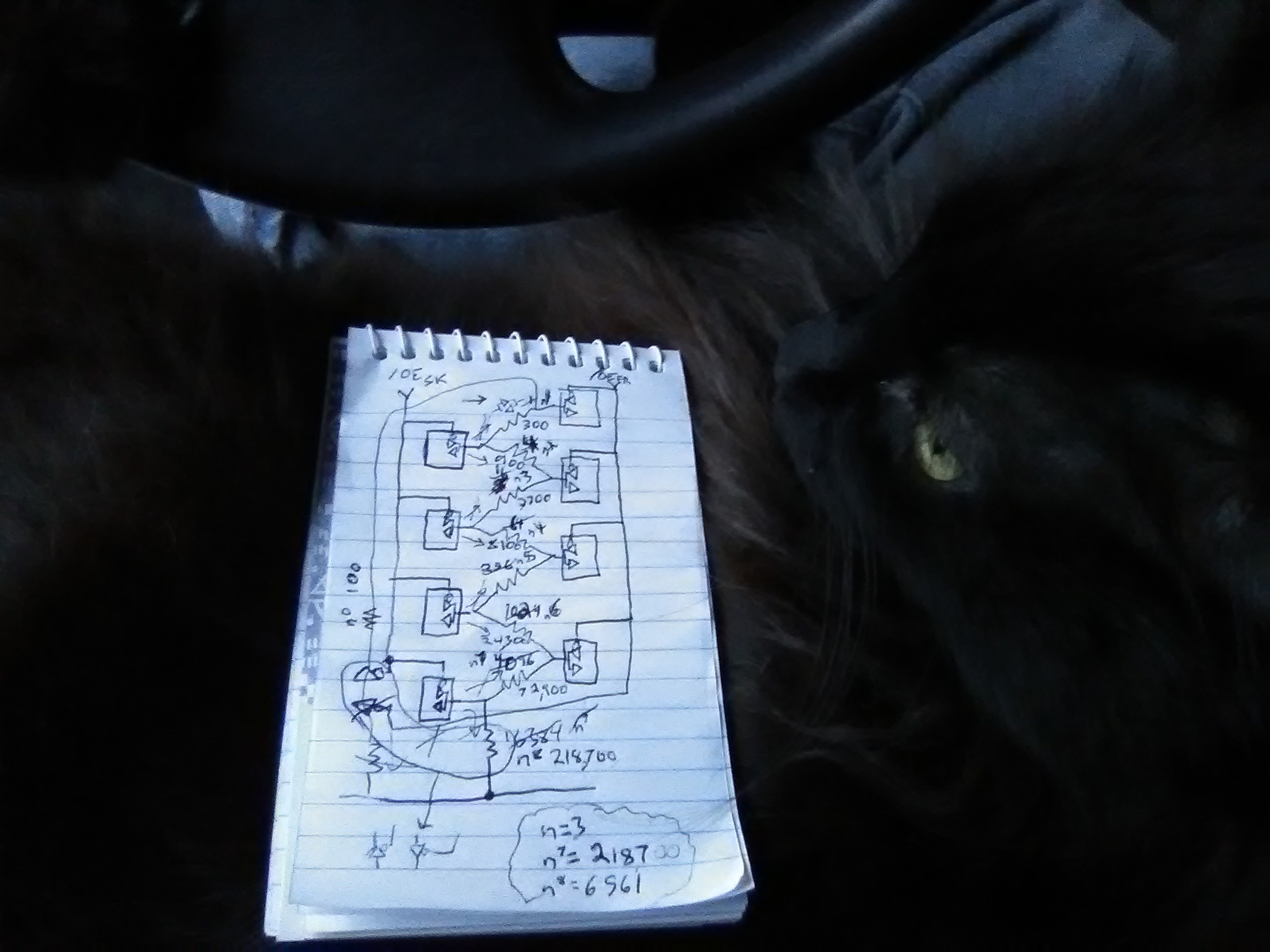
    Vague idea: since trying to interface with an 8-bit bus, maybe read-back of the sampled 32bits could happen by a sort of bucket-brigade. [And maybe similar for writing the free-runner?]. E.g. read the first chip, write from the second to the first, read the first again. Thus, plausibly reducing the number of chips [loading] on the bus, and plausibly the number of latches/buffers. 

    Also plausible, read first SK chip to bus, read second chip to FR first chip, etc. [Overwriting FR, but can be rewritten], a sort of left-right-forward bucket-brigade. [May be more feasible; since data I/Os are a single pin, loading wouldn't be reduced much if B4->B3->B2->B1, but would if B4s->B3f, B3f->B3s... erm, no...]

    BUT: B4-/\/\/-B3-/\/\/-B2-/\/\/-B1-/\/\/-Bus... hmmm. Only not-so-much, *maybe* since all SK chips [and all FR chips] use the same command signals [ [all chips reading/writing simultaneously] I Wonder, since read-commands and write commands take a different number of clock cycles, maybe a read's data would linger long enough to be registered by a write, hmmm. Could be handy elsewhere, too [copying FR commands/NOPs from bank to bank?] ]. 

    BUT: B4s-/\/\/-B3f-/\/\/-B3s-/\/\/-B2f-/\/\/...B1s-/\/\/-Bus... wouldn't have that limitation [read from SK, write to FR simultaneously should work]

    [Of course, B4s=1, B3s=0, B3f=0.5... hmmm.... resistor values increase left to right? Diodes? Buffers, of course, but then more control signals /OE, when sampling, no?]

    Ideally, would also reduce the number of control signals necessary to select which byte to read-back [knowing they'll always be read in order]... a sort of byte-wide shift-register.

    ---

    8 devices attached to a bus with only one buffer [two slightly preferable]. A shift-register, of sorts...

    ---

    Ahhhh...

    But this overwrites one side's data with the other's.

    It works[?], in this case because the Sidekick's data is loaded from the sample inputs *not* from the bus, thus Read-only, from the bus's perspective. Whereas the Free-Runner is [or could be] write-only from the bus's perspective. 

    Sample-data can be destroyed upon read-back AND when writing the Free-Runner. Free-Runner data can be shifted back in during either process. Weird.

    The resistors could be replaced with buffers with /OEs tied directly to the other /OE's... I spose that'd be easier to design. And still no extra control signals necessary. 

    But I'm a bit fixated on using passives; making use of the circuitry inherent to the devices... dunno why. And resistor-nets are a *tiny* bit cheaper, no?

    ----

    And more pondering... I think it requires a DQ latch to store the new FreeRunner data to be shifted in while shifting the data from the SideKick into the other FreeRunner registers... because, at that same time, the last SideKick register is also outputting to the bus [so can't contain the new FR data simultaneously].

    Here we have a new dilemma... with another shift-reg comes another control signal [though "strobe" may be necessary elsewhere anyhow]. So, another option is to sacrifice 8 bits of sample-inputs to use as that register. Wastes a lot of memory and brings the sample inputs down to 24 from 32... but, easier to...

    Read more »

  • Wouldja lookie there

    Eric Hertz09/20/2017 at 23:45 0 comments

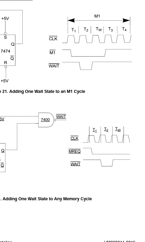
    as an aside at #Floppy "Fun" -- Backing up a unique Kay-Pro disk ... I just happened across this:

    Heh... guess I'm pretty good at (eventually) reinventing the wheel.

    Those are from the z80 datasheet.

  • Random Updates...

    Eric Hertz01/19/2017 at 03:47 0 comments

    UPDATE: Apparently I've found a general-spec... See the bottom

    -------

    sdramThingZero is still on-hold, but of course still runs 'round the ol' back of the head... There's nothing really stopping progress, just haven't gotten around to designing/ordering PCBs. In fact, the breadboarded sdramThingZero is still sitting on my desk right under my monitors.

    ------

    So here's something interesting:

    Does that look familiar, at all?

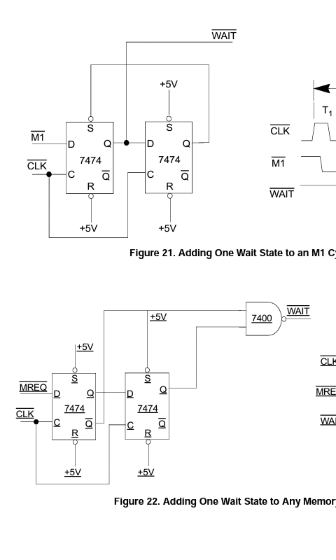
    Yep, it's pretty much exactly the same topology as the "one-shot" logic used in this project. Two flip-flops in series, both receiving (in some form) the input, performing some logic on the original and the delayed/latched output, and even an async-input (similar to my "one-shot Bypass" input). This is from the Intel 8284 datasheet, that's the clock-generator used for PC/XT (8088) computers. Besides clock-generation, the 8284's other key feature is what we see here, synchronizing an asynchronous "READY" signal to the system-clock... Just like my one-shots synchronize an asynchronous Chip-Select or Clock-Enable signal to the SDRAM's clock.

    Why's this interesting to me...? Maybe this is some sort of de-facto topology used all the time...? The fact is, I designed that circuit without having looked it up... I used knowledge of what was going in and expectations of what I wanted out, and I designed a circuit to do-so. I knew it *would* work, for the most-part (what happens if the asynchronous input comes between the setup/hold times? TI's thoughts here), but I didn't expect that it was good 'nough for a product. And yet, there it is!

    ------------

    SDRAM initialization:

    Note, first, I'm no trained expert... this is all what I've gathered in my experience with hacking SDRAMs... (single-data-rate, NOT dual-data-rate!)

    See also: https://sites.google.com/site/geekattempts/home-1/sdramthing/using-sdram

    Someone commented on my youtube-video, prompting me to respond that... basically... the SDRAM initialization-process, unfortunately, pretty much requires the entirety of the functions one might need to make use of the SDRAM, including ones that are otherwise unnecessary, and more.

    What do I mean...?

    Well, it's not like SRAM, where you can just turn it on, write a byte, and read it back (and you can repeat the write/read process at any other address, immediately thereafter).

    It's not like DRAM, where you can just turn it on, select a row-address, write a byte, and read it back (and you can repeat the select-row/write/read process at any other row/col-address the next time 'round).

    So what's it like...?
    Well, first, let's *merely* look at the write/read procedure.

    Note that this example differs from the SRAM/DRAM examples given earlier in that this can only happen *after* initialization, it can't be done immediately after power-up (we'll come back to that).

    To write a location and read-back you have to open a row (similar to DRAM), then you have to perform a write at your column, then you can read it back... That's pretty much the same as DRAM, except that if you want to do-so again at a different row, you have to explicitly choose to *close* the original row, first. (Closing a row is called "precharging").

    So, realistically the write/read-back procedure is similar to DRAM *unless* you want to access another row.

    But, we're just trying to do the *simplest* experiment, right...? Just to make sure we're wired-up correctly.

    (See Note1 below)

    So, say you're developing a *really simple* project, wherein all you want to do is write data, and read back... And, say 256 bytes is more than enough for you... (when opening a row, you have access to a minimum of 256 bytes/"columns" from that row at a time... some devices support up to 1024).

    Then you'd be set, you'd never have to think about precharging. (And, another cool side-effect is that as long as a row is open, it is inherently stored in registers rather than merely dynamic-RAM cells/leaky-capacitors, so needn't be refreshed... Handy!). BUT, you *would* have to consider the fact that you can't "activate"...

    Read more »

  • On Hold... + Great Quote.

    Eric Hertz12/08/2016 at 17:00 0 comments

    Not sure what my last log was, but this project has been put on-hold, as I've managed to bump some wires, or something, causing it to be much less reliable than it was previously. Time to PCBify, or at least point-to-point-solder it. And haven't had that kinda energy.

    In the meantime I leave you with this quote I stumbled upon, might say a bit about me:

    "SDRAM represents clinical levels of insanity to initialize" -- @Samuel A. Falvo II

    (https://hackaday.io/project/10035/log/49829)

  • FAIL, sorta expected...

    Eric Hertz11/22/2016 at 10:59 4 comments

    In the last log was a TODO:

    TODO: Believe it or not I did all that layout without actually verifying the chips I have match those footprints. Usually that'd be the *first* thing I'd do... Usually I'd make my own, in fact, because I rarely trust those provided. This time, for some reason my brain's been on this tetris-style packing-kick. Could be risky. I guess we'll see. I can feel the datasheet-lookup energy building... may be a few days. Or maybe I'll just print the danged thing and set my chips on the printout.

    Whelp, I printed it out... and it turns out it was risky.

    Out of 7 footprints I chose and laid-out, only 3 were correct.

    The 20-pin 7400-series SOICs in my collection are *wide*... Easy enough to fix since it's laid-out on breadboard.

    The 56-pin SSOP is 0.5mm spacing, not 0.4mm... Whelp, that was a lot of work for nuthin.

    The clock-generator chip is actually SSOP-10 (?!) not SSOP-8, and... I dunno what spacing, smaller than 0.4mm, it seems.

    ........

    I suppose I should take a step back and re-evaluate this ordeal... Maybe I'll spend a few days cleaning the apartment, first.

    Or maybe I'll just go play some Tetris... My gameboy's long-gone, and I'm tired of staring at the TV/monitors... I hate using my phone's touchscreen for things like this...

    But I just happened to save one of those ridiculous cheapo hand-held games from the 90's with the custom LCDs, and it just happens to have Tetris on it... Time to dig out the file and scouring-pads and dig through the box of batteries.

  • solder-proto for the next-generation

    Eric Hertz11/21/2016 at 20:22 0 comments

    Apparently it's brain-dump time.

    In the previous log I showed my thoughts on making a sorta general-purpose prototype-board that can be used for the first soldered prototype, as well as be used/usable for many other unrelated projects...

    Here's the latest fixation... Weee!

    What I didn't mention was how this proto-board also looks to the future of *this* project...

    This project has two main phases, I see...

    First is getting it as fully-functional (sample/repeat, high-speed, trigger, adjustable sample-frequency) as I can... That's easiest done with a uC that has plenty of GPIO pins... Thus I'm using my trusty ol' ATmega8515 40pin-DIPs... and, as I described in the last log, that lays-out perfectly over some otherwise currently-unnecessary breakout-space on my protoboard-design...

    The second phase is replacing the dedicated AVR in favor of whatever host one might want to use... e.g. a single-board computer like the Raspberry Pi, or even via an FT2232 chip connecting it directly to your computer via USB. The hurdle, here, is that this requires whittling down the number of required GPIOs to something reasonable... like an 8 or 16-bit data-bus.

    There's plenty of contemplation in my various logs regarding how I'll do that, and I don't doubt that I've got it mostly-figured-out... I could probably, if my brain works in my favor for that long, whip it out in less time than it'd take to receive this PCB order.

    But, I guess, I tend to take an iterative-approach with my projects, rather'n going gung-ho with a design->PCB... And, the current scenario is that the solderless-breadboarded prototype has become increasingly-flakey (largely, I'm sure, due to wires getting bumped, "antennae" everywhere, etc...(interestingly, when I run it at 50MHz, it interferes with my TV reception!))... The likelihood of this guy lasting a year and being able to just power it up and make use of it is... pretty low.

    So, iteratively, I still have a bit I could experiment with and implement while connected to an AVR... and, I wouldn't mind having a reliable prototype that I can come back to later down the line and turn on and expect to still work.

    -------

    Oy, all that explanation to say... no, I haven't forgotten about the second-phase, in this proto-board's design.

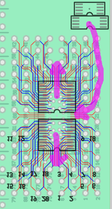
    Whittling down the GPIO-necessity is mostly just a matter of a bunch of latches... and low-and-behold, I've laid out this board for two 8bitters... Right under where the AVR goes, currently. And, again, I'll be using *two* of these boards for a single DIMM, so I'll have four 8bit latches available and broken-out. And, again, I've laid out SOIC-breakouts as well, 20pinners, which will also work for 74xx574 latches. So... I think we're set. And if not, then I can just as easily throw a third board at it. (Yay buying in quantities!)

    In fact, who knows, I might just bypass the AVR soldered-proto... It's plausible. I do have a PiZero and now also an LCD with HDMI, after all! And I plan to order an HDMI cable/adapter alongside this PCB-order... So, who knows.

    --------

    The image above shows the current state of the 574 breakout(s)... It wasn't easy fitting them in there, being that the other side is a TSSOP-80/56 breakout, but it wasn't particularly difficult, either. It was easier than I expected, though. A pleasant surprise, for sure.

    I *think* I might be able to squeeze that 8-pin TSSOP in between, but that might be almost as much work as the two 20pinners, and plausbly not possible, due to the number and positions of the vias and the red-traces necessary for the current setup.

    The idea, there, is to throw in the clock-generator chip... (also explained in previous logs)... That guy basically allows one to select from a huge selection of clock-frequencies anywhere from 500Hz to 200MHz (thus, sample-frequencies). Could be quite the gizmo, and I haven't yet experimented with it.

    (Also, it requires I2C, which I'm not expecting the "host" to provide, meaning I might be implementing it via bit-banging via the host-interface, or...

    Read more »

  • solder-proto

    Eric Hertz11/21/2016 at 13:17 8 comments

    UPDATE -- New SOIC-breakout... see below.

    Working on a solderable-prototype... due to solderless-breadboard-wiring-wonkiness.

    Decided not to design a full-on PCB, yet, as it's still in the prototyping-stage...

    Decided on 70mm x 70mm boards, they're much cheaper than the width necessary for a DIMM, so I'll "cludge" two together... It's actually pretty easy and stable with thin PCB-material to just overlap them for one or two rows.

    So, the board design is somewhat generic.

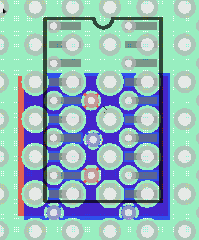
    First things first, the DIMM socket will solder into two 70mm tall boards with this running from end-to-end:

    Might take a little hand-drilling for the support-mounts, etc. But I'm more than OK with that.

    The thing about the DIMM sockets is that they have this weird footprint with diagonals... more on that in a bit.

    Next we have some breakout for surface-mount chips, since 7400's in the speeds we're looking for mostly only come in SSOP, or if you're lucky (as a prototyper) SOIC.

    (Yes, this is a breakout, for prototyping. No these traces are not matched-length, and who knows what kind of signal-issues may arise due to their closeness to each other).

    Now, you might look at that layout and go "whhhaaaa??!"

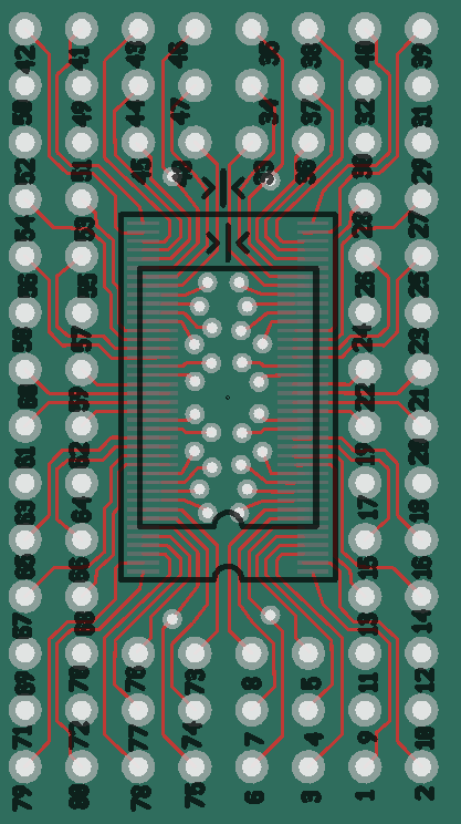
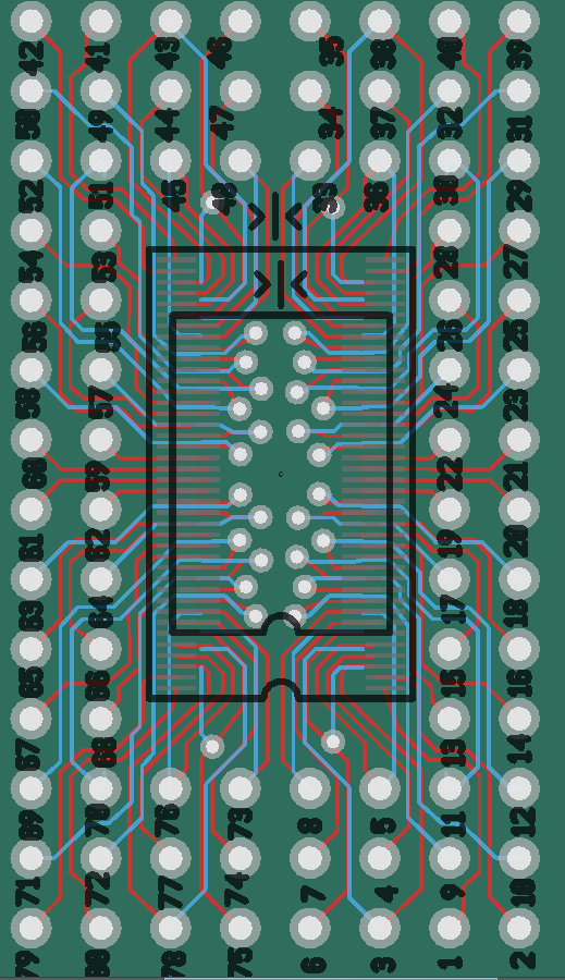
    But check this out... If I'mma make a prototyping-board and have ten of 'em made, I'mma think of other projects as well... So the above was designed *after* (on the other side of) this:

    I don't actually have any SSOP80 chips, that I'm aware of, but I do have some TSSOP56's I'd been planning on using... So this'll break that out nicely, and leave room for later prototypes.

    (If you have better ideas how to label the "pin numbers" to accomodate an arrangement like this, I'm all ears. I've thought about A1-A9, B1-9, etc... just to make it clear that these numbers *don't* correspond to the pin-numbers on the likely-smaller chips that'll be installed. I know better, but've been caught slipping-up on TQFP100 adapters fitted with smaller devices).

    Again you might say "whhhaaa?!" at the breakout-layout/numbering... Herein, the layout is specifically-designed to occupy as little space as possible while *also* being easily "straddled" with a 32-pin DIP, or even 40-pin, yahknow, with a few extra holes at the ends.

    So, that may seem a bit ridiculous, but consider sdramThingZero's parts-tally so far... We've got a 40-pin DIP (AVR), a SSOP-20 (74xx574 latch), and two SOIC-14's (74x00 NANDs). (Though, since this's been designed, I might opt for SSOP-14's in future orders). And, again, consider that this single board-design will be used *twice* to handle the DIMM socket... On one board, I can throw the AVR over the above layout and not waste a whole bunch of holes under the DIP.. On the other board, I can already handle two of my three 7400-series chips... again in that same workspace.

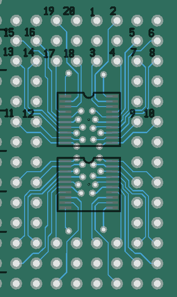
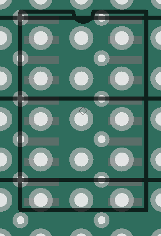
    And, I'm currently working on a more generic SOIC-breakout... Which isn't too-difficult considering they're half the space of regular breadboard spacing... meaning that when they're not populated, that space can be used as regular 'ol breadboard:

    So, the SOIC can be placed, it's a bit easier to solder to a via than directly to a pin... and it makes for backside-wiring, which I usually prefer. Note, again, if I don't need to place a SOIC, then that entire space can be used just like regular ol' 0.1in breadboarding-space. Should also work quite well with e.g. SOT-3, no?

    Then, there's the "center vias" I thought Ted was talking about in the comments, below... But he was talking about different ones. These center-vias alternatingly attach to "planes" on the top and bottom layers, making it easy to essentially have power and ground-planes on a 2-layer board, and easy to "solder-blob" most pins directly to 'em, or insert surface-mount decoupling-caps, pull-resistors, etc. on the back-side.

    Debating the use of octagonal vs circular pins/vias... also experimenting with the planes' violating the DRC trace-width rules...

    ---------

    So, this, like all my soldered-breadboard prototypes, will be wired point-to-point with "wire-wrapping"...

    Read more »

  • Trigger-Handler 2.0!

    Eric Hertz11/10/2016 at 22:35 2 comments

    DUH!

    Brief recap (better explained in past logs):

    A portion of the sample-memory will be used for a circular pre-buffer. Then, when a trigger is detected, it will jump out of the circular-buffer and begin sampling in the remaining memory.

    So the idea is to load the "Free-runner" (memory-controller) with two sequential "Activate [row]" commands... The first would activate the next row within the circular pre-buffer, the second would activate the first row *outside* the pre-buffer. But: Only *one* of these "Activate [row]" commands would be executed, depending on whether the trigger's been detected.

    This, previously, was handled by only outputting One "Chip-Select" signal for the two "Activate" commands, alongside only the *first* Activate command. The second would then be "Inhibited."

    The trigger, then, would control a MUX, which can selectively delay that "Chip-Select" by one clock-cycle. So, when the Trigger has occurred, that chip-select which was originally alongside the first "Activate" command, will now be delayed to execute the *second* "Activate" command, causing the system to exit from the circular pre-buffer, and enter into the sequential sample-memory.

    Here's a *simplified* example from a while-back. (Note that /CSLoop and /CSTriggered should be wired-together for a single /CS input to the circuit):

    (Note, this has issues with the case where the trigger occurs *exactly* between the two "Activate" commands, but that has been handled in previous logs. The concept is still the same; selectively delay the input /CS signal).

    This concept should work.

    BUT:

    After the trigger occurs, this system will delay *all* the chip-selects for *all* the commands... Including Read/Write commands. That's OK-ish... So, just repeat each command twice, only one would be executed... no biggie.

    I could get into the nitty-gritty details of how the "Free-Runner" (memory-controller) works, again, but I've gone over that in numerous previous logs. But, because of how it works, there remains one slight hurdle... Most commands can be shifted, slightly, without causing trouble. But there are two commands which actually (ideally?) have to occur back-to-back. The "Read" command tells the Free-Runner to begin executing commands from the next memory-page, and the "Write" command tells the sample-memory to sample data at its next memory-page.

    (This works because the Read command has an inherent "Latency"... it doesn't start until a couple clock-cycles later, whereas the Write command has no latency, it begins immediately. Thus the two commands can be executed at different times, but will actually *start* at the same time, keeping the Free-Runner and Side-Kick synchronized).

    All that to say, if I delay the chip-select after the trigger occurs, then I'd have to have two read-commands, followed by two write-commands, but since the read-command and write-command actually (ideally?) have to occur at specific times, the trigger-handler would affect that. They couldn't be back-to-back. It could be worked-around, but not ideal.

    Then BIG DUH:

    I really only need to delay the "Activate" command... Or, rather, I really only need to *select* one of two activate-commands... The other commands would, ideally, be left-alone...

    So, BIG DUH:

    The command-inputs are /RAS ("Row-Address Strobe"), /CAS ("Column-Address Strobe"), and /WE ("Write Enable"). of course, those can be "inhibited" when /CS ("Chip Select") is inactive...

    Those, basically, cover the major functions of the memory: Activating a Row and Reading/Writing a column.

    And, then, there's NOP... Which is functionally-identical to an "Inhibited" command, except occurs when /CS is *active*... Hmmmmmm

    NOP just *happens* to be what happens when all the active-low command-inputs are *inactive*, but again with /CS active.

    And /RAS just *happens* to be used for... Strobing a Row-Address... Hmm, like, maybe... "Activating a row"?

    Is it possible the *only* command-signal that needs to be activated to switch from NOP to "Activate [row]" is the...

    Read more »

View all 55 project logs

  • 1
    Step 1

    Unless you're a masochist, DON'T FOLLOW THESE INSTRUCTIONS. They are not ready... even as a follow-along, as described later. Check out the "Instructions Status" in the last "instruction"... That's all outdated, too.


    NOTE: These instructions are *in no way* complete enough for a functioning sdramThingZero, yet... But I'll add to them as my own prototype progresses. You're welcome to follow along! (lemme know if you do!)

    This Prototype is a low-speed version... probably limited to something like 16MHz due to being built on a solderless breadboard... Faster sampling will definitely be achievable with a custom PCB... but that's a ways off.

    I'll try to make these instructions as general-purpose as possible (for whatever SDRAM DIMM you may choose).

  • 2
    Step 2

    Select a DIMM:

    • SDRAM (PC-66, PC100, PC133...).
    • Preferably SINGLE-SIDED (for this prototype)
      • Double-sided DIMMs will only have half their memory available to this sdramThingZero prototype
    • Sorry, DDR++ support is a long ways off (if at all).
    • SODIMMs (from laptops) are not yet "supported"...

    (Note: For This Prototype I'm using Kingston ValueRam KVR-PC100/32, also marked: 9902384-003.A00 558111 on another sticker and four chips on a single-side marked VG3664164-IDT 04532391U -7L and, more importantly, the PCB is marked 2022364-002 A00

    #sdramThing4.5 "Logic Analyzer", which used the same DIMM since v2.0 used a DIMM simply labelled "PC133 128MB". 8 chips on one side marked ARC USA ARC4V128S30DTP-7 16MX8T3 0052. PCB marked: B6781A

    sdramThing1.0 seems to have vanished into thin-air... I'll try to remember to list its markings when I find it next. However, it didn't make use of the "Side-Kick" (it only used the first 32 data-bits) which is necessary for sdramThingZero.

    Note that it's probably *not* enough to just rely on the markings/stickers, as what really matters is the PCB-layout... Check the "oddities" below. You're a hacker, right? Get out your multimeter!

    For sdramThingZero, the important factor is that there are two separate chip-selects used per side... And I've only run into ONE DIMM that didn't meet that spec. The remainder of the notes, below, are a bit overkill. The odds you'll come across a 168pin DRAM DIMM (not SDRAM) is *quite low* unless you've worked with servers or really high-end workstations, plausibly Macintoshes, or got hand-me-downs from someone who did).

    Avoiding oddities (I've encountered):

    Make sure you actually picked an SDRAM DIMM!

    • It should have a "Serial Presence Detect" EEPROM (8-pin chip on the right-side
      • If not, it's probably a DRAM DIMM (yep, they exist), which will not work
      • If you got it from an old Pentium++ Workstation/PC (rather'n a server), you're probably alright...
    • It should have 84 "pins" on each side with a separator between pins 10 and 11 and another between pins 40 and 41
      • Higher pin-counts probably indicate DDR++, which again is not supported.
    • It should only have 4, 8, or 16 identical ICs in addition to the EEPROM)
      • Additional (non-identical) ICs likely indicates buffered or registered-DIMMs which are not supported
      • If it has e.g 9 identical ICs, it's likely ECC, which should work fine
        • Hey! More bits! Whatcha gonna do with all them bits?
    • Those SDRAM ICs should most-likely have tightly-spaced pins, and a lot of 'em, while also being quite thin (if they're as thick as a DIP, then they're most likely DRAM)
      • If in doubt, try searching for the part-number on those chips...
      • These stupid DRAM DIMMs are rare, but somehow I wound up with as many of them as SDRAM DIMMs... Sorry for making a big deal of it.

    The DIMM must make use of at least two *separate* Chip-Selects:

    1. Get out the multimeter
    2. Verify that there are no shorts between pins 30, 45, 114, and 129
      1. (I have no idea how that manufacturer got away with calling it "PC-100," how it worked at all in many systems, nor how we haven't heard more about a lot of fried motherboards)
      2. (Hey! If you happen to have a double-sided DIMM with 30 shorted to 45, and 114 to 129, but not between 30 and 114, then you might've just found the perfect use for an otherwise shitty DIMM that should never be installed on a motherboard! But I won't go into the details of how to make it work with sdramThingZero, as it's probably rather rare)
    3. Verify that there are two chip-selects, each connected to half of the available ICs:
      1. Put one multimeter probe on Pin30
      2. Slide the other down the pins on each chip until you hear a beep.
      3. Pin30 should be connected to one pin on half of the SDRAM ICs
      4. Do the same for Pin45, it should be connected to the remaining ICs
      5. NOTE: AND BIG TODO:
        1. The chip-selects may be connected to alternating ICs, or e.g.
        2. One chip-select may be connected to four ICs on the left and the other to the four on the right. (NOTE: This is per the Intel PC SDRAM Unbuffered DIMM Specification, located in my 'files section')
        3. This is a BIG TODO: Depending on which chips they're routed to, and more importantly which *byte* pins those chips connect-to, the sdramThingZero wiring may need to be changed accordingly! Hmmmm... The PC100 spec, Section 5, shows that /S0 should route to the ICs associated with DQ0-15 and DQ32-47 (which are on opposite sides of the PCB) and /S2 should route to the ICs associated with DQ16-31 and DQ48-63, this would correspond to the CS's being grouped into "left" and "right" groupings, rather than alternating. Though I have definitely seen alternating. Huh.

    This is my pinout used in sdramThing3.0-4.5 Note the groupings of the Chip-Selects with their associated bytes. #sdramThing4.5 "Logic Analyzer" used an 8-chip single-sided DIMM. This first prototype for sdramThingZero will use a 4-chip single-sided DIMM (due to supplies), the Chip-Select->Byte-Mapping appears to match.

    (Only look at this for the pinout/mapping of the DIMM... this is the *old* schematic... new schematics are in the following steps).

  • 3
    Step 3

    Plan your approach

    For this early prototype, I plan to use a solderless-breadboard...

    I won't be making use of all 32 bits that could be used for logic-analyzing... maybe just a handful for now, I don't feel like soldering *all those pins* for this proof-of-concept. (That's best left for a PCB!)

    Looking again at the image, above, you can see there are still quite a few pins to be soldered-up...

    So, how am I going to connect this thing to the breadboard?

    Normal breadboard-wires are pretty heavy-duty, soldering them directly to the DIMM's pins will most-likely rip up the pins (aka "Pads") after a while. So, it's a good thing to consider.

    I happen to have a bunch of thinner solid copper wire from old phone-wiring... This stuff works well in new breadboards, but old worn-out breadboards may not make a tight contact with these wires... So, again, think about what you've got to work with...

    If anything's gonna fail first, it'll be at the connections!

View all 9 instructions

Enjoy this project?

Share

Discussions

milahu wrote 10/25/2020 at 19:18 point

has anyone tried to scale this?

1. in terms of memory size, for example 4 x 1024 MB total memory, giving 2 GB payload size. or even more crazy: use the SDRAM as "state machine memory" to generate address signals, and write the payload data to an SSD hard drive, connected via SATA3 (500 MB/s) or M.2-NVMe (2 GB/s) - no filesystem, just write the raw data to consecutive addresses. use two or more SDRAM modules to decouple write/read operations (like video memory)

2. in terms of frequency, what [esot.eric] calls >>"DDR" emulation: Simply connect two opposite-edge-triggered D-latches to each input-signal, fed into two separate SDRAM pins, and now we're talking 16ch 266MS/s :)<<. how would i distribute/rotate the input signals to get 4 x 133 MHz = 533 MHz? (or even more)

also, could this work with an external clock? so we have synchronous sampling, and can avoid oversampling

  Are you sure? yes | no

clae wrote 12/03/2018 at 14:30 point

Two thoughts:

An [n] bit logic analyzer is only a resistor ladder away from being an [n] bit analog to digital converter ... or a [x] channel [n/x] bit ADC.

Second thought is a little more vague, but slowly forming up in my mind: run this in "reverse" as a fast video card for old/new slow 8 bit computers - ie, fill the RAM with image data during the h-blank and / or v-blank, tri-state it off the main bus, and then free-run it out to a VGA (or whatever) port at the required speed to keep up with the display device.  

  Are you sure? yes | no

Eric Hertz wrote 12/03/2018 at 16:20 point

I like your thinking!

I'll have to look up resistor-ladder ADCs, but I'm vaguely-familiar with resistor-ladder DACs, which could certainly be combined with your free-running VGA idea.

If you haven't already checked-out the prior versions of sdramThing, you might cement some of those vague-ideas over there. 

Though, Maybe consider this a spoiler-warning, as it seems your gears are already churning in paths best-left to churn on their own and come up with great new/different ideas!

 #sdramThing4.5 "Logic Analyzer" is the immediate precursor to this sdramThingZero. It, in a sense, acts as a combined logic-analyzer *and* raster-video driver. A weird way of showing waveforms, and highly "hacked" to double for sample/repeat.

The previous versions 1.0-2.0 are hosted on another site, (TODO: link! I think it can be found at the 3.5 page)

There I go into quite a bit of rambling about the possibilities.

Also, 1.0 is *much* simpler to implement, with a tiny bit more CPU overhead during 'pseudo' free-running, though limited to the CPU frequency. Its first purpose was driving a raster-based parallel-RGB TFT, and later an LVDS-interfaced TFT (slowing the bit clock to 1/7th the CPU speed). These slow refresh-rates are possible with direct-to-panel interfacing to TFTs.

For VGA, of course, timing/refresh-rates are much less forgiving... Full-on Free-running with asynchronous CPU vs. SDRAM clocks, as in v2.0+, may be necessary for those speeds. (TODO: what's the pixel-clock for 640x480x60Hz? greater than, say, an AVR's 20MHz?) Or, more-certainly, for higher resolutions.

But: there's a TL:DR (and major spoiler) for yah:

I think it was www.tinyvga.com that introduced me to the "burst" concept in SDRAM. That basically handled 512 horizontal pixels, but only because that was the burst-limit of his chip. Chips with 1024-column bursts exist. 640x480 should be easy-enough, no "free-running" nor fed-back signals necessary! 1024x768, even.

  Are you sure? yes | no

ksemedical wrote 02/01/2017 at 11:34 point

WOW, truly impressive. I have a few things I am trying to work on, but one side issue is the need of a logic analyzer, this is great work from both real practical and fundamentally interesting (you seem to be at "one-with-" fast fourier transform ha ha (really, great work, I saw some of your soldering handiwork in your pics which is amazing by itself, but this is really great work, and you clearly did very well working with (and recognizing) the other folks (this is really a quite deep project crossing all kinds of normal category barriers. Cool stuff, and I will try to make my needed logic analyzer following this project..... hat's off bro, great stuff

  Are you sure? yes | no

Rogan Dawes wrote 08/31/2016 at 19:53 point

This may be a stupid question, but I hope that I have managed to understand how this works enough to not make a fool of myself!

I'm trying to find ways to capture video from a PC. After using something like a TVP7002 chip to handle the video signal, and turn it into a parallel bit stream (or an equivalent HDMI transceiver/decoder), one then needs to actually do something with that data. That generally requires something capable of really fast sampling, in order to keep up with the video signal.

Would it be possible to have the parallel bitstream feeding in to the SDRAM data lines, and the sync bits used to clock the address lines, so that the video data is written to the SDRAM as long as the appropriate signals are present? My thinking is that when the controller decides that it wants to read in a frame, it would set a line high. This, in combination with the "start of frame" signal (i.e. VSYNC or similar), would then trigger the free running of the SDRAM acquisition, until end of frame. Capture would then stop. At this point, the controller would be informed via an interrupt that a frame had been captured, and could then read it out at leisure, and do whatever is required.

Does this sound feasible?

  Are you sure? yes | no

Eric Hertz wrote 09/01/2016 at 02:31 point

Absolutely!

Some great thought-points in here, as well. I want to get back to you on this when I've got a bit more time. There's a "Star" And "Unread" in my inbox.

But I wanted to say, I think you're spot-on in your understanding of how it works and how it can be made-use-of. 

Totally awesome, thanks!

  Are you sure? yes | no

Rogan Dawes wrote 09/01/2016 at 03:20 point

Excellent! Glad to know I have the basic concept down, even if the details are a mystery! :-)

It's something I've been trying to solve for ages, a cheap KVM, essentially. With this technique, your frame rate is limited only by the rate at which you can send the frames to the client. Enough SDRAM to cache two frames allows for sending only differences, a la VNC.

  Are you sure? yes | no

James Newton wrote 08/08/2016 at 17:56 point

Is there a specific SDRAM that we could purchase which you are pretty sure would work? e.g. is the SDRAM you are using for the prototype available? Or is there an available SDRAM that you think would match the requirements?

  Are you sure? yes | no

Eric Hertz wrote 08/11/2016 at 19:43 point

Great question... why aren't I listing the models I've worked with...? I'll throw the current model in the instructions "Selecting a DIMM" section... and think about how to approach a list later down the road.

When I get around to designing a PCB, I'll definitely be taking into account flexibility with most *standard* DIMMs (though, things like shorted Chip-Selects from *really shitty* quality-control I can't help).

Thanks for this thought-point. Because of it, I actually took a different route with this prototype than the instructions (and prior versions), using a DIMM socket rather'n soldering directly, so I can test compatibility amongst all the modules I've got. I'll be posting that soon.

  Are you sure? yes | no

Kurt Roesener wrote 08/03/2016 at 06:10 point

I really look forward to see how this project progresses.

Especially since I still have a bunch of these sticks just laying around  ;)

  Are you sure? yes | no

Eric Hertz wrote 08/05/2016 at 12:09 point

Woot! Thanks for the motivation! 

In my mind, it's already done... The mods from the already-functional #sdramThing4.5 "Logic Analyzer" to make this possible are minor. But... (aside from the sampling-speed improvements) a large part of the point of this "version" is to make it more easily approachable to others. I think it's time to focus on that aspect, and worry about speed later. Thanks for reminding me of that!

And, lo-and-behold, focussing on the "approachability-factor," rather'n speed, means I can use 74xx-series parts already in my collection (from the 80's!) , rather'n having to buy high-speed LVTTL chips :)

After all these revisions, I'm looking at either breaking up some 128MB matched-pairs or using a 32MB DIMM... and as backwards as it may sound, I think I want to keep that matched-pair for my socket-7 mobo in case I ever want to revisit the ol' ISA slots/cards... (and the much-more-sophisticated BIOS settings it offers over my newer systems). 

So, sdramThingZero's prototype may well be much smaller than the prior prototypes... but that's only due to available (unhacked) supplies. And, of course, once this prototype is running (and documented?) Moving on to 133MS/s, a custom PCB, a tremendous amount of more sample-space, and more will be in the works.

  Are you sure? yes | no

jlbrian7 wrote 07/21/2016 at 01:06 point

I just read the blog.  Good job!

  Are you sure? yes | no

Eric Hertz wrote 07/21/2016 at 03:27 point

Woot! Thanks, bro!

  Are you sure? yes | no

Nimajamin wrote 04/06/2016 at 15:42 point

Fabulous!! This screams to me as being a fundamental tech/technique.. Given that Fpga's are built up of Look Up Tables that are used in this way, with numerous examples of the BRAM blocks in Spartan-6's being used for Fifo's, Serialisers, State Machines, etc.. to name a few. 

Now we've gone from approx 4k to 64Mb!! Awesome stuff. Hats off to you! I'm sure this could be used to build a great many things. :))

  Are you sure? yes | no

Eric Hertz wrote 04/07/2016 at 03:31 point

Hey, right on! I'll have to look more into this BRAM thing. There, of course, is quite a bit of external work to get an SDRAM to look like a gigantic lookup-table, but now that you mention it, it wouldn't be *that* difficult to, say, have two separate address-busses (for rows/cols) broken out to make it look like one *really huge* lookup-table (as opposed to thousands of selectable 1024-byte lookup-tables).

Got me thinking, yo!

  Are you sure? yes | no

davedarko wrote 03/13/2016 at 16:21 point

thinking form factor here, may some old notebook sdram might work as well?

  Are you sure? yes | no

Eric Hertz wrote 03/13/2016 at 16:23 point

Indeed, just saw an image of a PiZero with someone holding it, and realized the SDRAM would be quite a bit larger... (Crazy!)

SODIMM might be a great option, especially if this goes somewhere beyond my workbench... But I think my proto will use DIMM since... quantities.

  Are you sure? yes | no

Vikas V wrote 03/13/2016 at 15:57 point

Neat idea Eric. I think this might be the way to go. It also helps that SDRAM sticks/modules are available at throwaway prices. Ultra cool !

  Are you sure? yes | no

Eric Hertz wrote 03/13/2016 at 16:21 point

Cool, thanks yo! But don't be deterred from trying it the other way! This is one of those "fits together with my other project..." moments, had to take it :) 

Thanks for all the insight on your #Logic analyzer using raspberry pi

  Are you sure? yes | no

Similar Projects

Does this project spark your interest?

Become a member to follow this project and never miss any updates