Reed Foster
-
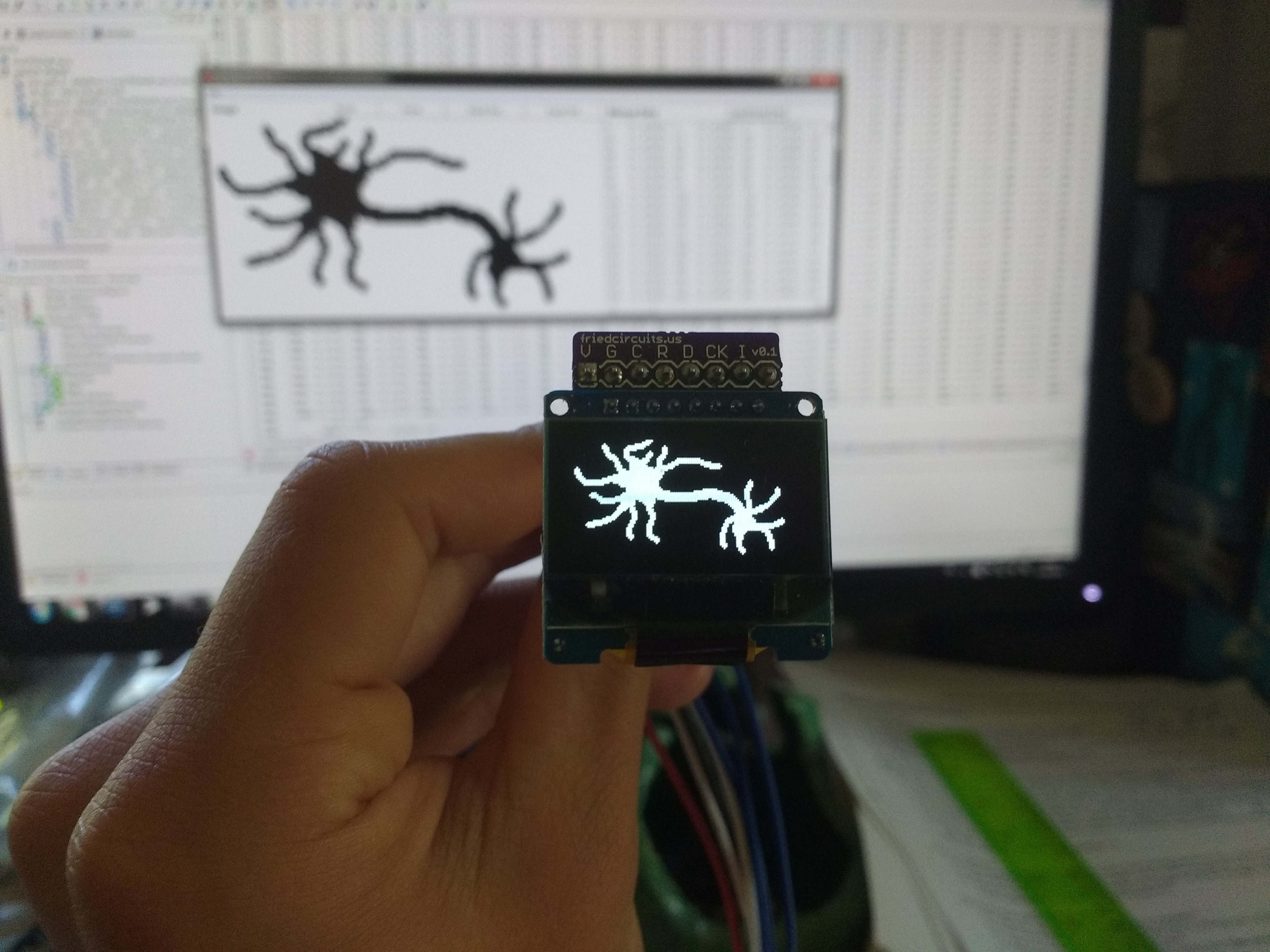
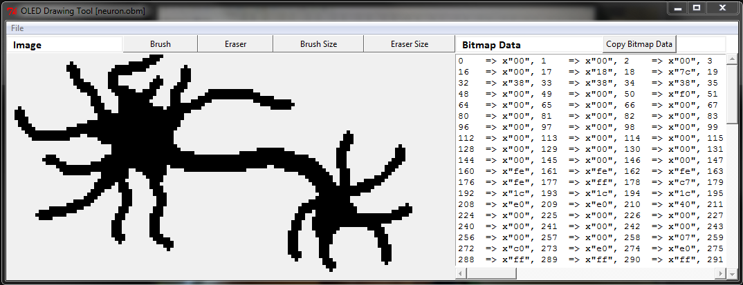
Drawing Bitmaps with Python
05/29/2016 at 21:27 • 0 commentsAs soon as I discovered that I would have to run a script to convert .xbm files to an array that would be usable by SSD1306, I decided that I would write a simple python application to import .xbm files, draw new ones, and export the display data to an array with VHDL syntax. It took a while to get the GUI to work how I wanted, but eventually the app worked:
![]()
Screenshot:
![]()
Python code is uploading to Github
-
When In Doubt, Software!
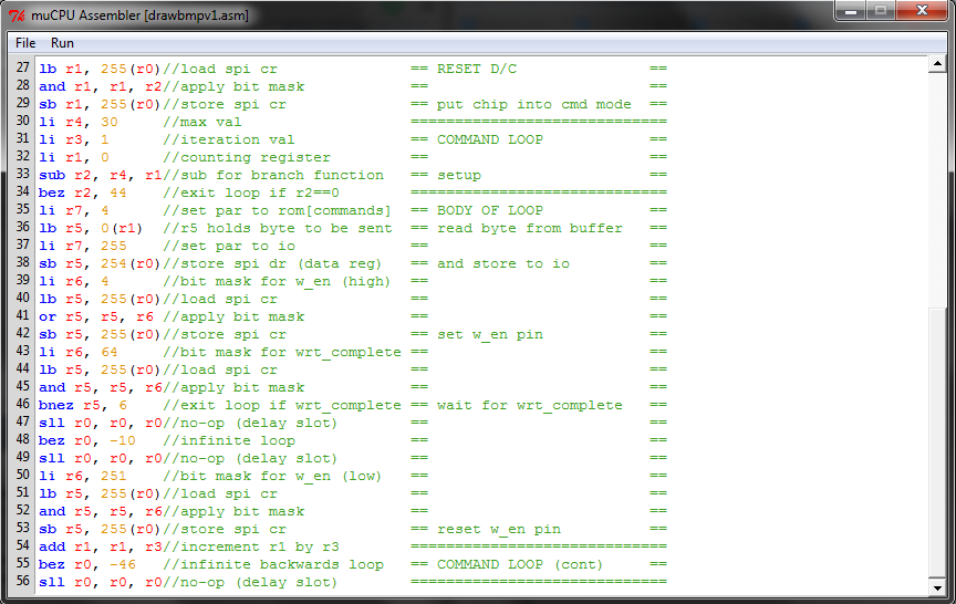
05/27/2016 at 03:38 • 0 commentsWith an almost complete loss of data between the SPI controller and the SSD1306, I decided that I should use just the processor core because I know that at least the processor core runs how it is supposed to (how the simulation runs) on the FPGA itself. With software SPI, I ran into a whole new set of problems. With an 8 bit immediate width, branch instructions cannot cover very much code. Furthermore, a loop that executes 256 times is not possible, so one cycle of the loop must be unfolded. By controlling the io ports with software and unfolding a loop, my code space had grown so large that the outer loop (I have 3 nested loops) was so wide I could not branch from end to end. The solution: add intermediate branches. Pseudo-code:
jmp 2; skips next two instructions when loop is executed
     ; they are only executed when branched/jumped to from
     ; elsewhere in the program
jmp outerloop_start; intermediate for backwards jump
jmp outerloop_exit; intermediate for exit branch
When I was using the vhdl SPI controller, one of the clear indicators that the SSD1306 wasn't receiving all of the data was the dimness of the screen. I did a couple tests with an arduino, and when I disabled the charge-pump configurations, the display was unlit connected to 3.3v and only very dim with 5v. I have yet to figure out why the display was able to receive some commands and not others, but I eventually will troubleshoot that with a logic analyzer or something like that.
Using this indicator, I was able to tell whether or not the software SPI worked fairly easily. Unfortunately, it took me forever to figure out what was going wrong after the initialization; there wasn't any comprehensible data that appeared on the display. I tested a pattern of bytes that I expected would fill the top row only, but found a much different result; the 16 bytes that I sent were arranged vertically.
![]()
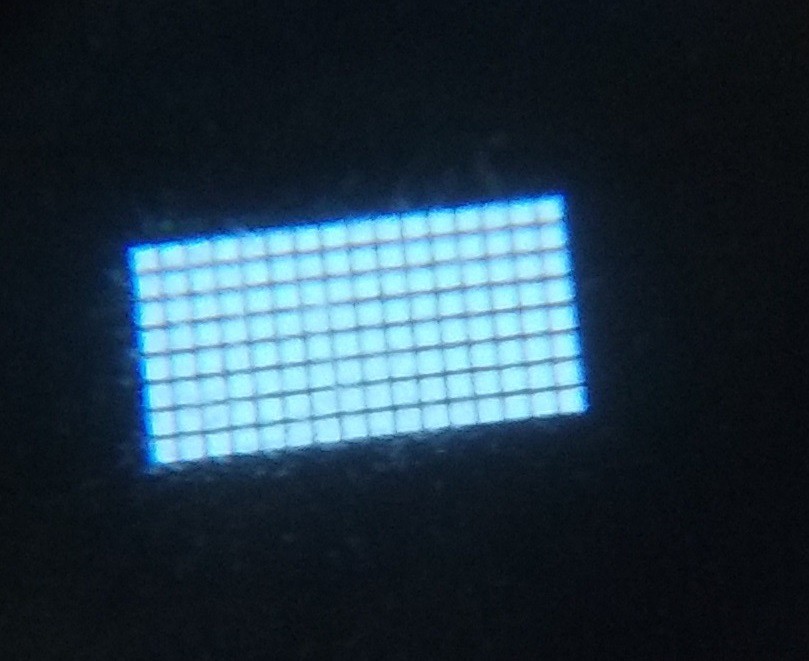
After discovering this, I looked at the datasheet for the SSD1306 and discovered that I simply misunderstood how the device was interpreting the data I sent it. After visiting stackexchange for a couple conversion methods between hex and binary strings in python, I produced a simple program that remaps the bits in the .xbm file format (the one that I had been using to draw and save black and white images) to bits that can be sent, byte by byte, to the SSD1306 without additional processing on the FPGA. The end result:
![]()
Zoomed in (I augmented my phone camera with a small lens from an ancient video camera). Individual pixels are visible.
![]()
Assembler code:
//PortD pin assignments (nc means no connection)
//assignment     set-bitmask (or)    reset-bitmask (and)
//pin0 => mosi   00000001 | 1        11111110 | 254
//pin1 => sclk   00000010 | 2        11111101 | 253
//pin2 => dc     00000100 | 4        11111011 | 251
//pin3 => rst    00001000 | 8        11110111 | 247
//pin4 => ss     00010000 | 16       11101111 | 239
//
		//SET RST and SS (rst, ss = 1)
		li r7, 255    //set par (page address register) to io bank
		li r2, 24     //bit mask for rst (high)
		lb r1, 255(r0)//load spi reg
		or r1, r1, r2 //apply bit mask
		sb r1, 255(r0)//store spi reg
		//RESET RST (rst = 0)
		li r2, 247    //bit mask for rst (low)
		lb r1, 255(r0)//load spi reg
		and r1, r1, r2//apply bit mask
		sb r1, 255(r0)//store spi reg
		// DELAY LOOP (loops for ~4us to hold reset low for length required by ssd1306)
		// while (true) {
		//  if (i = 10) {break;}
		//  else {i++};
		// }
		li r4, 10         //r4 is stopval
		li r3, 1          //r3 is incrementval
		li r1, 0          //r1 is counting reg
delay_start:		sub r2, r4, r1    //r2 compares r4 and r1; if neg, then r1 > r4; if zero, r1 = r4
		bez r2, delay_exit//if r2==0, then exit loop
		nop               //delay slot
		bez r0, delay_start//infinite backwards loop
		add r1, r1, r3    //increment r1 by r3
		//SET RST (rst = 1)
delay_exit:		li r2, 8      //bit mask for rst (high)
		lb r1, 255(r0)//load spi reg
		or r1, r1, r2 //apply bit mask
		sb r1, 255(r0)//store spi reg
		//RESET D/C (d/c = 0; put ssd1306 into command mode, which it should already be in)
		li r2, 251    //bit mask for d/c
		lb r1, 255(r0)//load spi reg
		and r1, r1, r2//apply bit mask
		sb r1, 255(r0)//store spi reg
		//COMMAND LOOP (sends 25 init commands + 6 memory config commands; prepare ssd1306 for buffwrite)
		// while (true) {
		//   if (i = 31) {break;}
		//   else {
		//     ss = 0
		//     while (true) {
		//       if (j = 8) {break;}
		//       else {
		//         sclk = 0;
		//         mosi = byte[j];
		//         sclk = 1;
		//       }
		//     }
		//     ss = 1;
		//   }
		//loop setup
		li r1, 0      //r1 is counting reg
		li r3, 1      //r3 is incrementval
cmdloop_start:		li r4, 31     //r4 is stopval
		sub r2, r4, r1//r2 compares r4 and r1; if neg, then r1 > r4; if zero, r1 = r4
		bez r2, cmdloop_exit//if r2==0, then exit loop
		//loop contents
		li r7, 12     //set par to rom[commands]
		lb r6, 0(r1)  //r6 holds the byte to be send via spi
		li r7, 255    //set par back to io bank
		//reset ss
		li r5, 239    //bit mask to reset ss
		lb r4, 255(r0)//load spi reg
		and r4, r5, r4//apply bit mask
		sb r4, 255(r0)//store spi reg
		//send byte (loop)
		li r2, 0      //r2 is counting reg
cmdbyte_start:		li r4, 8      //r4 is stopval
		sub r5, r4, r2//r5 compares r4 and r2; if neg, then r2 > r4; if zero, r2 = r4
		bez r5, cmdbyte_exit//exit loop if r5==0
		nop           //delay slot
		//sclk low (setup mosi)
		li r5, 253    //bit mask to reset sclk
		lb r4, 255(r0)//load spi reg
		and r4, r5, r4//apply bit mask
		sb r4, 255(r0)//store spi reg
		//mosi
		//shift left unit desired bit is msb, then shift right 7; b7:b1=0, b0=desired bit
		sll r5, r6, r2//shift current bit to msb
		li r4, 7      //shamt for srl
		srl r5, r5, r4//shift msb to lsb
		lb r4, 255(r0)//load spi reg
		li r3, 254    //bitmask to reset mosi
		and r4, r4, r3//clear mosi bit of spi reg
		or r4, r5, r4 //combine spi reg with mosi_out
		sb r4, 255(r0)//store spi reg
		//sclk high (latch mosi)
		li r5, 2      //bit mask to set sclk
		lb r4, 255(r0)//load spi reg
		or r4, r5, r4 //appy bit mask
		sb r4, 255(r0)//store spi reg
		//end loop
		li r3, 1      //reset constant loop variables; r4 (stopval) reset later
		bez r0, cmdbyte_start//infinite backwards loop
		add r2, r2, r3//increment r2 by r3
		//set ss
cmdbyte_exit:		li r5, 16     //bit mask to set ss
		lb r4, 255(r0)//load spi reg
		or r4, r5, r4 //appy bit mask
		sb r4, 255(r0)//store spi reg
		//end loop
		li r3, 1      //reset constant loop variables; r4 (stopval) reset later
		bez r0, cmdloop_start//infinite backwards loop
		add r1, r1, r3//increment r1 by r3
		//SET D/C (d/c = 1; put ssd1306 into data mode)
cmdloop_exit:		li r7, 255    //set par to io bank
		li r2, 4      //bit mask for d/c
		lb r1, 255(r0)//load spi reg
		or r1, r1, r2 //apply bit mask
		sb r1, 255(r0)//store spi reg
		//DATA LOOP (sends 1024 bytes of data to gddram in ssd1306
		//
		// i = 0;
		// while (true) {
		//   r7 = i;
		//   r6 = mem(0);
		//   k = 0;
		//   cs = 0;
		//   while (true) {
		//     sclk = 0;
		//     mosi = r6(k);
		//     sclk = 1;
		//     k++;
		//     if (k == 8) {break;}
		//   }
		//   cs = 1;
		//   j = 1;
		//   while (true) {
		//     cs = 0;
		//     k = 0;
		//     while (true) {
		//       sclk = 0;
		//       mosi = r6(k);
		//       sclk = 1;
		//       k++;
		//       if (k == 8) {break;}
		//     }
		//     cs = 1;
		//     j++;
		//     if (j == 0) {break;}
		//   }
		//   i++;
		//   if (i == 12) {break;}
		// }
		li r7, 8      //set par to rom[data]
		li r1, 8      //r1 is counting reg (initialized to same value as par)
		li r4, 1      //r4 is countval
outloop_start:		li r5, 12     //r5 is stopval
		sub r6, r5, r1//r6 compares r5 and r1; if neg, then r1 > r5; if zero, r1 = r5
		bez r6, itrfwd//exit loop if stopval is reached
		nop           //delay slot
		//r6 = byte to send
		li r2, 0      //bleh
		add r7, r1, r0//set par to rom[data]
		lb r6, 0(r2)  //r6 holds the byte to be send via spi
		li r7, 255    //set par back to io bank
		//reset ss
		li r5, 239    //bit mask to reset ss
		lb r4, 255(r0)//load spi reg
		and r4, r5, r4//apply bit mask
		sb r4, 255(r0)//store spi reg
		//send byte (loop)
		li r3, 0      //r3 is counting reg
dbyte_start:		li r5, 8      //r5 is stopval
		sub r4, r5, r3//r6 compares r5 and r3; if neg, then r3 > r5; if zero, r3 = r5
		bez r4, dbyte_exit//exit loop if r5==0
		nop           //delay slot
		//sclk low (setup mosi)
		li r5, 253    //bit mask to reset sclk
		lb r4, 255(r0)//load spi reg
		and r4, r5, r4//apply bit mask
		sb r4, 255(r0)//store spi reg
		//mosi
		//shift left unit desired bit is msb, then shift right 7; b7:b1=0, b0=desired bit
		sll r5, r6, r3//shift current bit to msb
		li r4, 7      //shamt for srl
		srl r5, r5, r4//shift msb to lsb
		lb r4, 255(r0)//load spi reg
		li r7, 254    //bitmask to reset mosi
		and r4, r4, r7//clear mosi bit of spi reg
		or r4, r5, r4 //combine spi reg with mosi_out
		li r7, 255    //set par to io bank
		sb r4, 255(r0)//store spi reg
		//sclk high (latch mosi)
		li r5, 2      //bit mask to set sclk
		lb r4, 255(r0)//load spi reg
		or r4, r5, r4 //appy bit mask
		sb r4, 255(r0)//store spi reg
		//end loop
		li r4, 1      //reset constant loop variables; r5 (stopval) reset later
		bez r0, dbyte_start//infinite backwards loop
		add r3, r3, r4//increment r3 by r4
		//set ss
dbyte_exit:		li r5, 16     //bit mask to set ss
		lb r4, 255(r0)//load spi reg
		or r4, r5, r4 //appy bit mask
		sb r4, 255(r0)//store spi reg
		bez r0, 10     //skip intermediate branches, they are only executed when outer loop is repeated/exited
		nop
itrback:		bez r0, outloop_start //jump to start of outer loop
		nop
itrfwd:		bez r0, outloop_exit //jump to end of outer loop
		nop
		//inner loop
		li r2, 1      //r2 is countval
inloop_start:		bez r2, inloop_exit//exit loop if r2 overflowed
		//loop contents
		add r7, r1, r0//set par to rom[data]
		lb r6, 0(r2)  //r6 holds the byte to be send via spi
		li r7, 255    //set par back to io bank
		//reset ss
		li r5, 239    //bit mask to reset ss
		lb r4, 255(r0)//load spi reg
		and r4, r5, r4//apply bit mask
		sb r4, 255(r0)//store spi reg
		//send byte (loop)
		li r3, 0      //r3 is counting reg
lp_dbyte_start:	li r5, 8      //r5 is stopval
		sub r4, r5, r3//r6 compares r5 and r3; if neg, then r3 > r5; if zero, r3 = r5
		bez r4, lp_dbyte_exit//exit loop if r5==0
		nop           //delay slot
		//sclk low (setup mosi) #loopstart
		li r5, 253    //bit mask to reset sclk
		lb r4, 255(r0)//load spi reg
		and r4, r5, r4//apply bit mask
		sb r4, 255(r0)//store spi reg
		//mosi
		//shift left unit desired bit is msb, then shift right 7; b7:b1=0, b0=desired bit
		sll r5, r6, r3//shift current bit to msb
		li r4, 7      //shamt for srl
		srl r5, r5, r4//shift msb to lsb
		lb r4, 255(r0)//load spi reg
		li r7, 254    //bitmask to reset mosi
		and r4, r4, r7//clear mosi bit of spi reg
		or r4, r5, r4 //combine spi reg with mosi_out
		li r7, 255    //set par to io bank
		sb r4, 255(r0)//store spi reg
		//sclk high (latch mosi)
		li r5, 2      //bit mask to set sclk
		lb r4, 255(r0)//load spi reg
		or r4, r5, r4 //appy bit mask
		sb r4, 255(r0)//store spi reg
		//end loop #loopend
		li r4, 1      //reset constant loop variables; r5 (stopval) reset later
		bez r0, lp_dbyte_start//infinite backwards loop
		add r3, r3, r4//increment r3 by r4
		//set ss
lp_dbyte_exit:		li r5, 16     //bit mask to set ss
		lb r4, 255(r0)//load spi reg
		or r4, r5, r4 //appy bit mask
		sb r4, 255(r0)//store spi reg
		//end loop
		li r4, 1      //reset constant loop variables; r5 (stopval) reset later
		bez r0, inloop_start//infinite backwards loop
		add r2, r2, r4//increment r2 by r4
		//end loop
inloop_exit:		li r4, 1      //reset constant loop variables; r5 (stopval) reset later
		bez r0, itrback//infinite backwards loop
		add r1, r1, r4//increment r1 by r4
outloop_exit:		nop           //delay slot
end_program:		bez r0, end_program //halt command, processor idles in endless loop
Because of the complexity of the assembler code to display a still image, I'd probably have to add a j-type instruction or increase the instruction word size to display animations/video.
-
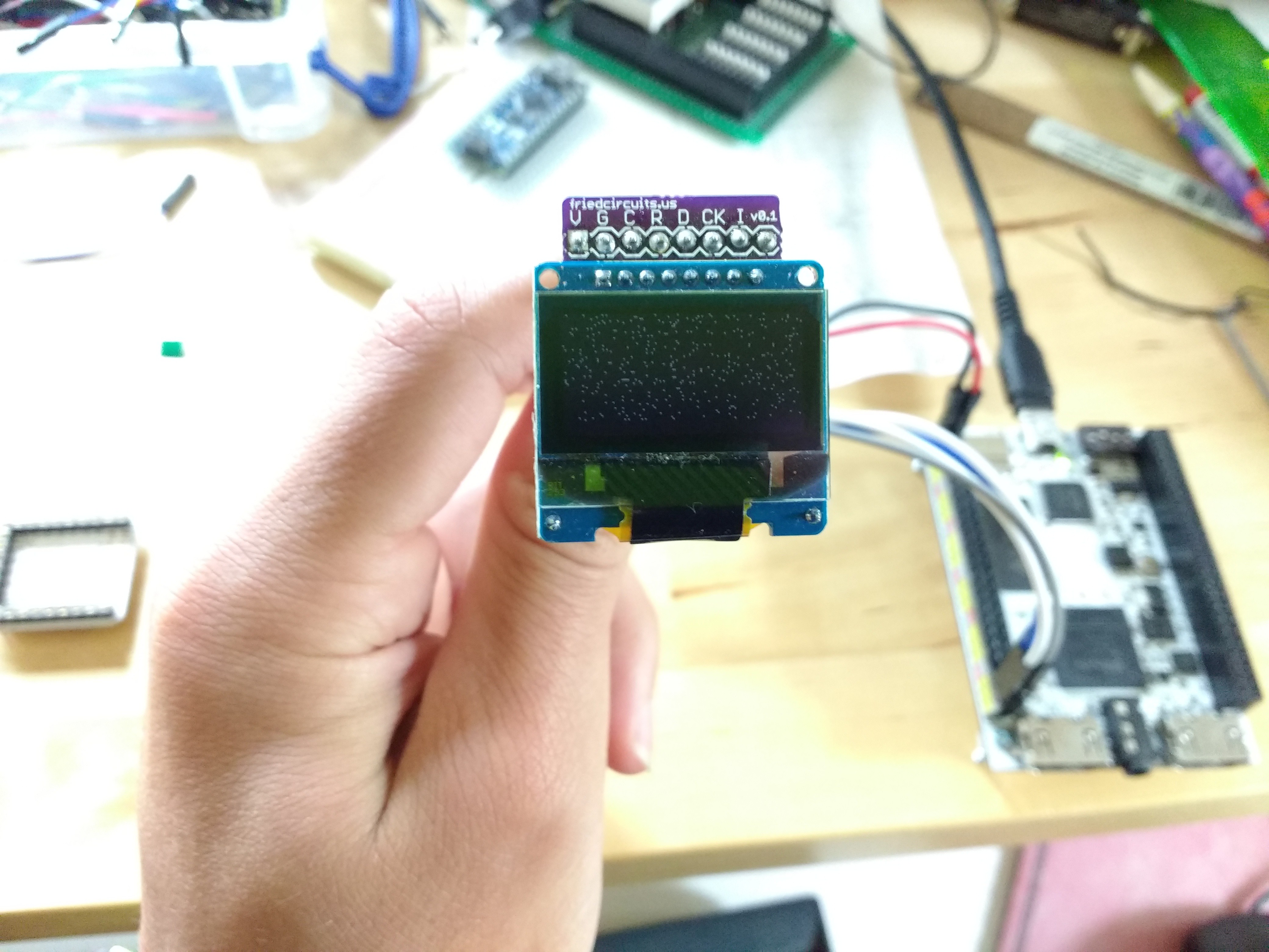
Potential Signs of Life
05/14/2016 at 23:48 • 0 commentsI wrote some vhdl to connect the core module to my spi module that I created, as well as some assembly code. Looking at the simulation waveform, the display should theoretically display a blank screen, but that was not the case. The clock and data are slow enough according to the ssd1306 spec sheet, but I'll try a slower clock later (the whole spi controller runs off of the divided clock, so slowing the sclk will introduce problems with the fifo which will require some redesign, otherwise I would have already done it). Even though it is far from working, it's still exciting to see pixels light up on the display. As usual, commentless :( vhdl code is up on github.
(side note: I have tested the display with an arduino, and it does work).
Picture of the display
![]()
SPI waveform
![]()
-
Lots of Updates
05/08/2016 at 20:46 • 0 commentsI've let some of the work I finished pile up, so here are several updates:
I redesigned the memory, which now uses a 16 bit address, and provides 4KiB of ROM, 4KiB of RAM, and 4B of I/O (maybe need some more). The upper byte of the address is determined by the page address register (r7). The lower byte is the same as the old method, 8 bit immediate plus the base address register specified in the opcode. This is (sometimes) annoying because it takes two instructions to access a location in memory. Most of the time, however, there is only one instruction to set r7, and each memory access requires only one instruction. This occurs when the data being accessed is somewhat densely packed in memory. When the data is spread out, then it takes about 2 instructions on average to access each byte.
I also decided to scrap the receive portion of the spi controller, and finished up the send portion. I did this because currently, I have no use for spi inputs (but probably will soon), and so it was difficult to determine exactly how I wanted the controller to behave.
Finally, I added several new instructions to the instruction set. I discovered that it was going to be a problem to write a program with lots of simple loops without a load immediate instruction. Before the load immediate instruction, each parameter of each loop was stored in a separate memory address. This made it rather complicated to write programs with more than just a few loops. This instruction, out of all of my other ones, is the least faithful to the MIPS instruction set. To load an immediate value in MIPS, one simply uses one of the many i-type instructions that MIPS supports and specifies r0 as the second operand (the immediate being the first one). However, due to my shortened instruction word, I only have 2 bits for opcode, which allows for 4 instructions. 2 of these are used by loads and stores, and the 3rd is used by r-type instructions, which have a 5 bit function code (32 functions). However, the load immediate requires an immediate value in the instruction word (duh...). To increase the amount of functions supported by an instruction with an immediate value, the second register address is used as another opcode (functionality that MIPS actually employs in some of its branch relative to zero instructions). I used this register field for my final (opcode of 0b10) instruction type. Prior to this iteration, I used 6 of the 8 available function codes with a 3 bit register address for branches. Now, the 7th function code is used for load immediates. Phew...hopefully that wasn't too boring. Upload to github coming soon.
On to screenshots:
Assembler with syntax highlighting and improved refresh features: i.e. An asterisk appears on either side of the filename at the top of the window when a key is pressed after the file has been saved or a new one has been opened. However, this includes arrow keys and nonprinting keys, so I'll probably fix this soon.
![]()
iSim waveform of SPI master (again, more for show than actual documentation):
![]()
-
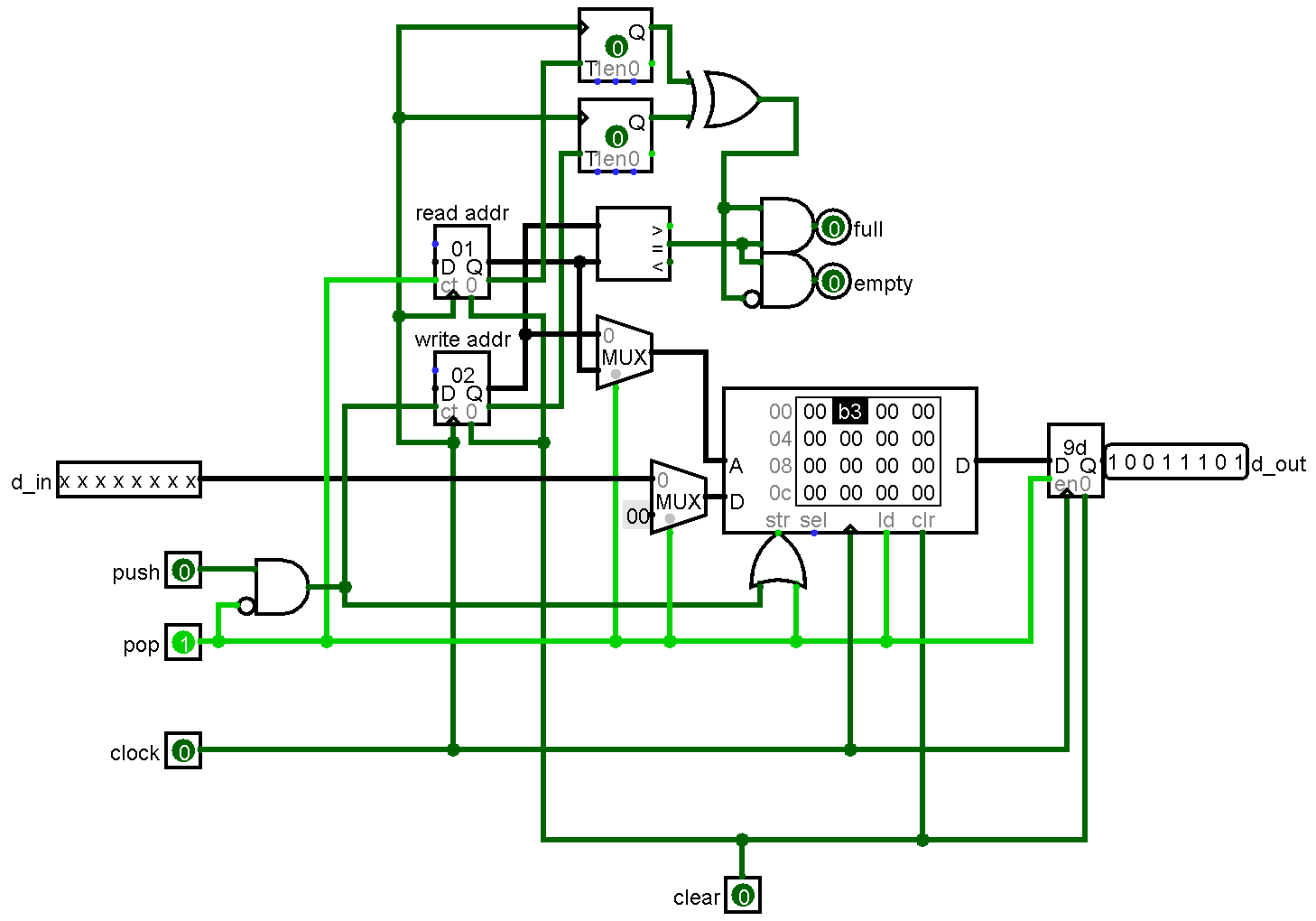
VHDL FIFO
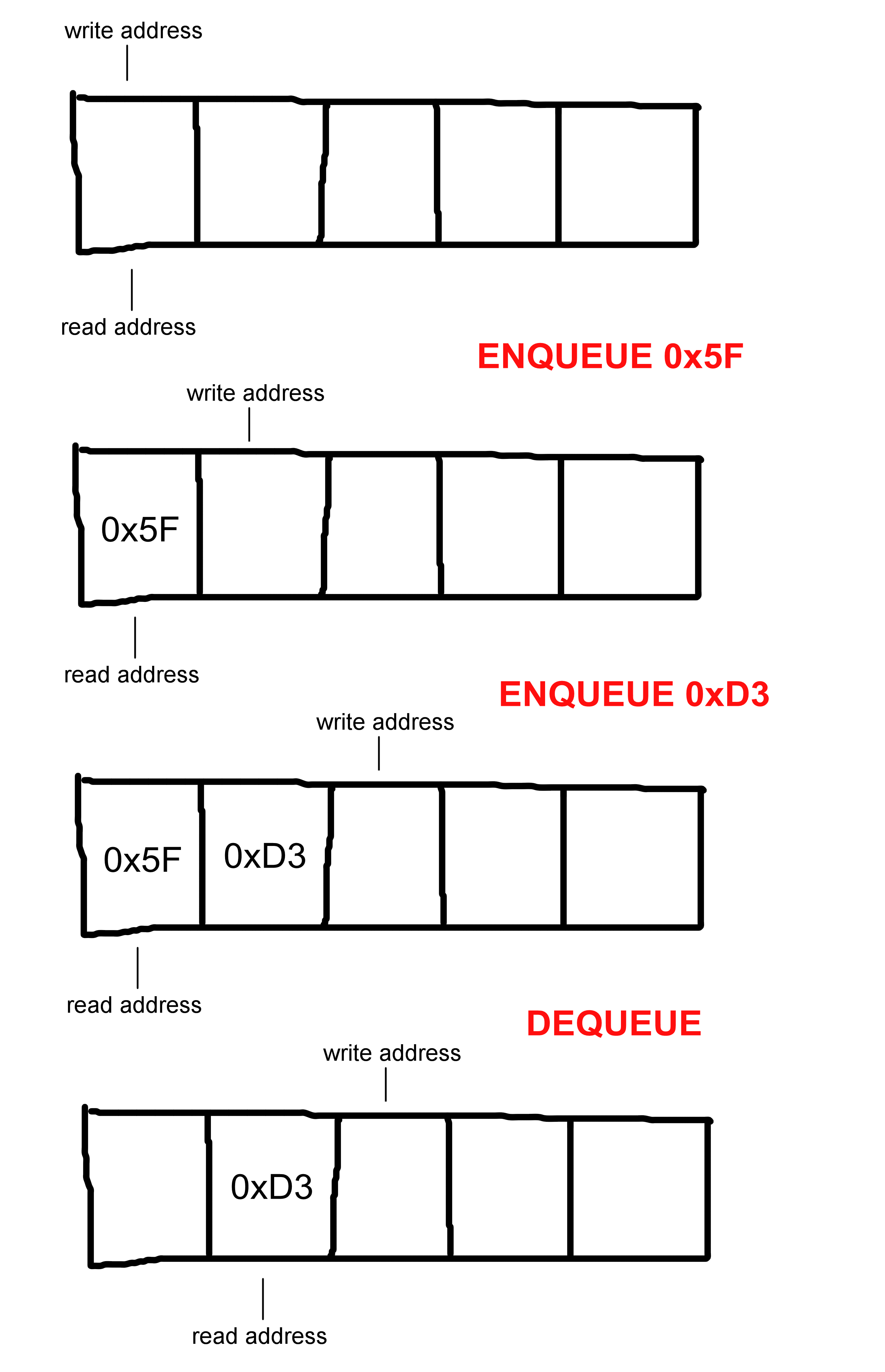
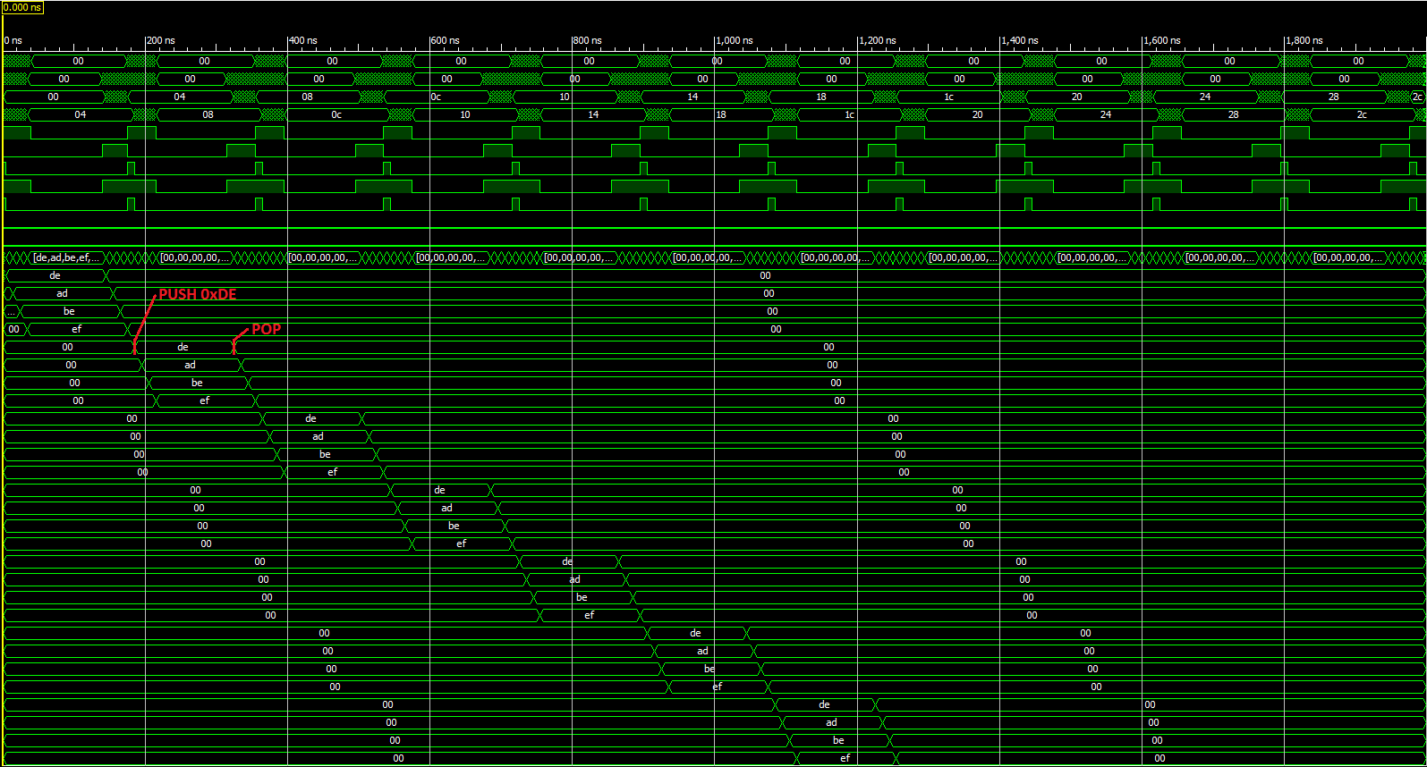
05/04/2016 at 00:15 • 3 commentsSlowly, but surely, the VHDL code for the controller is coming along; I've just finished a structural architecture for a FIFO queue (first in first out). In a FIFO, data is "enqueued" (pushed in a stack) and "dequeued" (popped in a stack). However, the cool thing about queues (and stacks, for that matter) is that only a value must be supplied; the stack handles addressing. Below is a sample of enqueueing and dequeueing using a FIFO queue:
![]()
iSim Waveform of FIFO simulation (vhdl on github)
![]()
-
Improved SPI I/O in Logisim
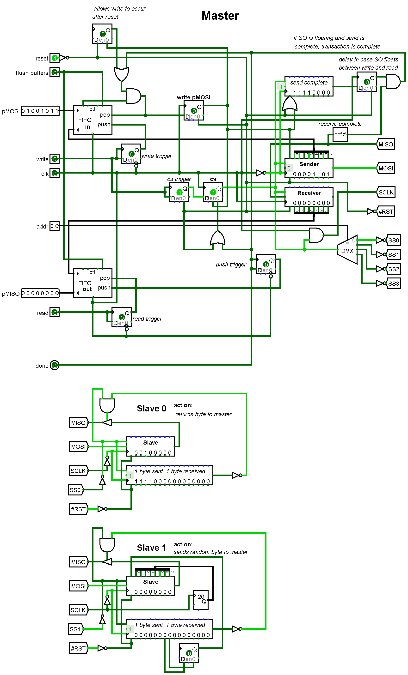
05/02/2016 at 00:13 • 0 commentsThis controller adds more functionality that the other lacked. The operation of the controller itself is almost entirely standalone and only requires an input of a clock signal and a steady address signal during operation. I added a FIFO to the input as well so that the data in the shift register is not overwritten when the write input pin is asserted. In addition, a D-FF is set whenever the write pin is asserted, and the flip-flop is only reset when the master has sent a byte and the slave is no longer sending data (might need changing depending on operation of slaves). The output of the D-FF is the cs signal, which is inverted for the ~cs line to the slave. Currently there are only two slaves; one sends the byte it receives back to the master, and the other sends a pseudorandom byte to the master. Here's the .circ file on Github.
SPI controller
![]()
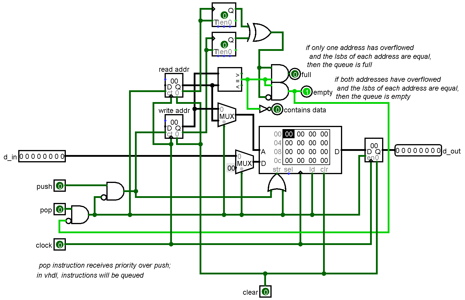
Updated FIFO:
![]()
-
SPI I/O in Logisim
04/28/2016 at 04:42 • 1 commentJust finished a design for the SPI controller in Logisim. The slave doesn't really do anything; it shifts out what was shifted in, so when I run the clock for a while, the FIFO fills up with 2 different byte values (master initialized to one value, slave to another). Both the read and write functions are synchronous; the master's shift register only loads from the parallel port when the clock rises and write is high. Similarly, the FIFO only pops the value at the read address when the clock rises and read is high. Currently, with the limited functionality of Logisim block RAM, the FIFO cannot be written to at the same time as it is being read from; this will change for the implementation in VHDL. SPI circuitry below:
![]()
FIFO stack (with less documentation of circuitry):
![]()
-
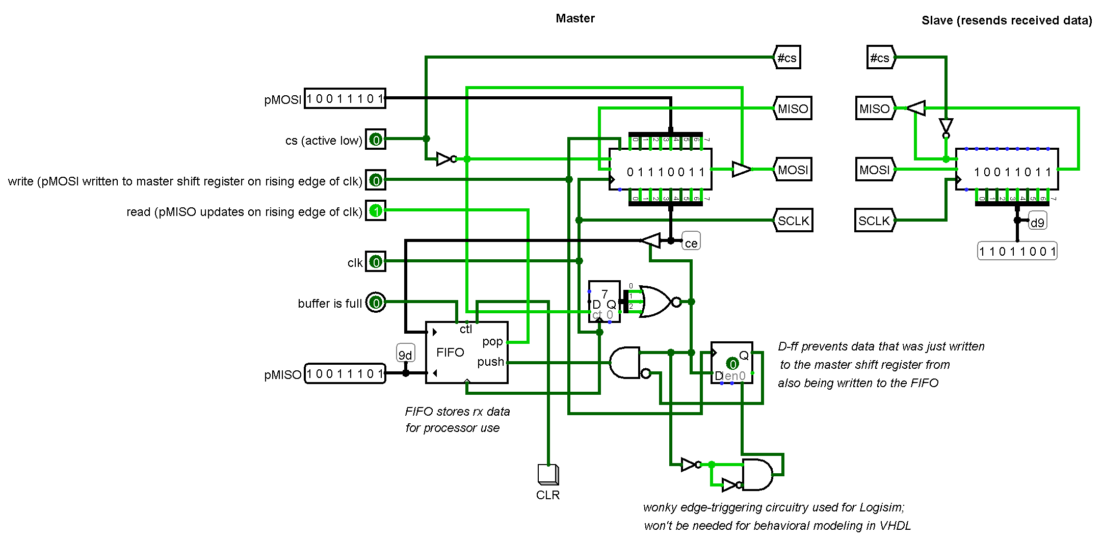
SPI I/O
04/28/2016 at 00:49 • 0 commentsI've decided to do away with the complicated video controller setup that I was starting to design. Instead of building what was going to effectively be a co-processor (with its own instruction set, memory, execution hardware...), I decided that I would leave it up to the processor to write the required bytes of data to the SPI controller. I will design a more generic SPI controller that supports input as well as output and 16 slaves (maybe more). I might still keep an external memory to store the initialization sequence for the display. For now, it's just an idea, code and schematics to come later...
-
Graphics Controller
04/18/2016 at 04:21 • 0 commentsTo provide data for the SPI master, a graphics controller is needed (otherwise the processor is bogged down with simple loads and stores). I built a circuit in Logisim that seems to do the job. I've uploaded the .circ file to github, and included a screenshot below:
![]()
-
MOAR I/O! (SPI)
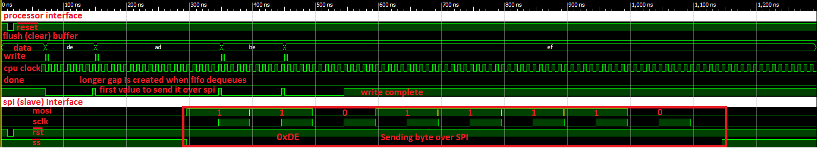
04/18/2016 at 00:05 • 0 commentsI have a couple oled displays lying around, and I figured that the display wouldn't be too complicated to interface to (riiiight). Anyway, the OLED controller (SSD1306) is configured to communicate with SPI, so to talk to it, I need an SPI master entity that takes an 8-bit parallel value and loads it (serially) into the OLED. I also wrote an arduino sketch based off of Adafruit's library for the SSD1306. By writing this sketch, it is easier for me to understand what exactly needs to happen to a) initialize the display and b) write data to it to display pixels (and hopefully characters and words eventually). The vhdl code I've written may not be the most efficient code, but it appears to work. I've uploaded the vhdl file for the SPI master (as well as its testbench) to github, and below is an (edited) image of the iSim waveform output:
iSim Waveform
![]()
Arduino Sketch
#define SSD1306_LCDWIDTH                  128
#define SSD1306_LCDHEIGHT                 64
#define SSD1306_SETCONTRAST 0x81
#define SSD1306_DISPLAYALLON_RESUME 0xA4
#define SSD1306_DISPLAYALLON 0xA5
#define SSD1306_NORMALDISPLAY 0xA6
#define SSD1306_INVERTDISPLAY 0xA7
#define SSD1306_DISPLAYOFF 0xAE
#define SSD1306_DISPLAYON 0xAF
#define SSD1306_SETDISPLAYOFFSET 0xD3
#define SSD1306_SETCOMPINS 0xDA
#define SSD1306_SETVCOMDETECT 0xDB
#define SSD1306_SETDISPLAYCLOCKDIV 0xD5
#define SSD1306_SETPRECHARGE 0xD9
#define SSD1306_SETMULTIPLEX 0xA8
#define SSD1306_SETLOWCOLUMN 0x00
#define SSD1306_SETHIGHCOLUMN 0x10
#define SSD1306_SETSTARTLINE 0x40
#define SSD1306_MEMORYMODE 0x20
#define SSD1306_COLUMNADDR 0x21
#define SSD1306_PAGEADDR   0x22
#define SSD1306_COMSCANINC 0xC0
#define SSD1306_COMSCANDEC 0xC8
#define SSD1306_SEGREMAP 0xA0
#define SSD1306_CHARGEPUMP 0x8D

//Pin Connections
#define OLED_MOSI   9
#define OLED_CLK   10
#define OLED_DC    11
#define OLED_CS    12
#define OLED_RESET 13

static uint8_t buff[SSD1306_LCDHEIGHT * SSD1306_LCDWIDTH / 8] = {
0x00, 0x00, 0x00, 0x00, 0x00, 0x00, 0x00, 0x00, 0x00, 0x00, 0x00, 0x00, 0x00, 0x00, 0x00, 0x00,
0x00, 0x00, 0x00, 0x00, 0x00, 0x00, 0x00, 0x00, 0x00, 0x00, 0x00, 0x00, 0x00, 0x00, 0x00, 0x00,
0x00, 0x00, 0x00, 0x00, 0x00, 0x00, 0x00, 0x00, 0x00, 0x00, 0x00, 0x00, 0x00, 0x00, 0x00, 0x00,
0x00, 0x00, 0x00, 0x00, 0x00, 0x00, 0x00, 0x00, 0x00, 0x00, 0x00, 0x00, 0x00, 0x00, 0x00, 0x80,
0x80, 0x80, 0x00, 0x00, 0x00, 0x00, 0x00, 0x00, 0x00, 0x00, 0x00, 0x00, 0x00, 0x00, 0x00, 0x00,
0x00, 0x80, 0x80, 0xC0, 0xC0, 0x00, 0x00, 0x00, 0x00, 0x00, 0x00, 0x00, 0x00, 0x00, 0x00, 0x00,
0x00, 0x00, 0x00, 0x00, 0x00, 0x00, 0x00, 0x00, 0x00, 0x00, 0x00, 0x00, 0x00, 0x00, 0x00, 0x00,
0x00, 0x00, 0x00, 0x00, 0x00, 0x00, 0x00, 0x00, 0x00, 0x00, 0x00, 0x00, 0x00, 0x00, 0x00, 0x00,
0x00, 0x00, 0x00, 0x00, 0x00, 0x00, 0x00, 0x00, 0x00, 0x00, 0x00, 0x00, 0x00, 0x00, 0x00, 0x00,
0x00, 0x00, 0x00, 0x00, 0x80, 0xC0, 0xE0, 0xF0, 0xF8, 0xFC, 0xF8, 0xE0, 0x00, 0x00, 0x00, 0x00,
0x00, 0x00, 0x00, 0x00, 0x00, 0x00, 0x00, 0x00, 0x00, 0x00, 0x00, 0x00, 0x00, 0x80, 0x80, 0x80,
0x80, 0x80, 0x00, 0x80, 0x80, 0x00, 0x00, 0x00, 0x00, 0x80, 0x80, 0x80, 0x80, 0x80, 0x00, 0xFF,
0xFF, 0xFF, 0x00, 0x00, 0x00, 0x00, 0x80, 0x80, 0x80, 0x80, 0x00, 0x00, 0x80, 0x80, 0x00, 0x00,
0x80, 0xFF, 0xFF, 0x80, 0x80, 0x00, 0x80, 0x80, 0x00, 0x80, 0x80, 0x80, 0x80, 0x00, 0x80, 0x80,
0x00, 0x00, 0x00, 0x00, 0x00, 0x80, 0x80, 0x00, 0x00, 0x8C, 0x8E, 0x84, 0x00, 0x00, 0x80, 0xF8,
0xF8, 0xF8, 0x80, 0x00, 0x00, 0x00, 0x00, 0x00, 0x00, 0x00, 0x00, 0x00, 0x00, 0x00, 0x00, 0x00,
0xF0, 0xF0, 0xF0, 0xF0, 0xF0, 0xF0, 0xF0, 0xF0, 0xF0, 0xF0, 0xF0, 0xF0, 0xE0, 0xE0, 0xC0, 0x80,
0x00, 0xE0, 0xFC, 0xFE, 0xFF, 0xFF, 0xFF, 0x7F, 0xFF, 0xFF, 0xFF, 0xFF, 0xFF, 0x00, 0x00, 0x00,
0x00, 0x00, 0x00, 0x00, 0x00, 0x00, 0x00, 0x00, 0x00, 0x00, 0x00, 0xFE, 0xFF, 0xC7, 0x01, 0x01,
0x01, 0x01, 0x83, 0xFF, 0xFF, 0x00, 0x00, 0x7C, 0xFE, 0xC7, 0x01, 0x01, 0x01, 0x01, 0x83, 0xFF,
0xFF, 0xFF, 0x00, 0x38, 0xFE, 0xC7, 0x83, 0x01, 0x01, 0x01, 0x83, 0xC7, 0xFF, 0xFF, 0x00, 0x00,
0x01, 0xFF, 0xFF, 0x01, 0x01, 0x00, 0xFF, 0xFF, 0x07, 0x01, 0x01, 0x01, 0x00, 0x00, 0x7F, 0xFF,
0x80, 0x00, 0x00, 0x00, 0xFF, 0xFF, 0x7F, 0x00, 0x00, 0xFF, 0xFF, 0xFF, 0x00, 0x00, 0x01, 0xFF,
0xFF, 0xFF, 0x01, 0x00, 0x00, 0x00, 0x00, 0x00, 0x00, 0x00, 0x00, 0x00, 0x00, 0x00, 0x00, 0x00,
0x03, 0x0F, 0x3F, 0x7F, 0x7F, 0xFF, 0xFF, 0xFF, 0xFF, 0xFF, 0xFF, 0xFF, 0xE7, 0xC7, 0xC7, 0x8F,
0x8F, 0x9F, 0xBF, 0xFF, 0xFF, 0xC3, 0xC0, 0xF0, 0xFF, 0xFF, 0xFF, 0xFF, 0xFF, 0xFC, 0xFC, 0xFC,
0xFC, 0xFC, 0xFC, 0xFC, 0xFC, 0xF8, 0xF8, 0xF0, 0xF0, 0xE0, 0xC0, 0x00, 0x01, 0x03, 0x03, 0x03,
0x03, 0x03, 0x01, 0x03, 0x03, 0x00, 0x00, 0x00, 0x00, 0x01, 0x03, 0x03, 0x03, 0x03, 0x01, 0x01,
0x03, 0x01, 0x00, 0x00, 0x00, 0x01, 0x03, 0x03, 0x03, 0x03, 0x01, 0x01, 0x03, 0x03, 0x00, 0x00,
0x00, 0x03, 0x03, 0x00, 0x00, 0x00, 0x03, 0x03, 0x00, 0x00, 0x00, 0x00, 0x00, 0x00, 0x00, 0x01,
0x03, 0x03, 0x03, 0x03, 0x03, 0x01, 0x00, 0x00, 0x00, 0x01, 0x03, 0x01, 0x00, 0x00, 0x00, 0x03,
0x03, 0x01, 0x00, 0x00, 0x00, 0x00, 0x00, 0x00, 0x00, 0x00, 0x00, 0x00, 0x00, 0x00, 0x00, 0x00,
0x00, 0x00, 0x00, 0x80, 0xC0, 0xE0, 0xF0, 0xF9, 0xFF, 0xFF, 0xFF, 0xFF, 0xFF, 0x3F, 0x1F, 0x0F,
0x87, 0xC7, 0xF7, 0xFF, 0xFF, 0x1F, 0x1F, 0x3D, 0xFC, 0xF8, 0xF8, 0xF8, 0xF8, 0x7C, 0x7D, 0xFF,
0xFF, 0xFF, 0xFF, 0xFF, 0xFF, 0xFF, 0xFF, 0x7F, 0x3F, 0x0F, 0x07, 0x00, 0x30, 0x30, 0x00, 0x00,
0x00, 0x00, 0x00, 0x00, 0x00, 0x00, 0x00, 0x00, 0x00, 0x00, 0x00, 0x00, 0x00, 0x00, 0x00, 0x00,
0x00, 0x00, 0x00, 0x00, 0xFE, 0xFE, 0xFC, 0x00, 0x00, 0x00, 0x00, 0x00, 0x00, 0x00, 0x00, 0x00,
0x00, 0x00, 0x00, 0x00, 0x00, 0x00, 0x00, 0x00, 0x00, 0x00, 0x00, 0x00, 0x00, 0xE0, 0xC0, 0x00,
0x00, 0x00, 0x00, 0x00, 0x00, 0x00, 0x00, 0x00, 0x00, 0x00, 0x30, 0x30, 0x00, 0x00, 0x00, 0x00,
0x00, 0x00, 0x00, 0x00, 0x00, 0x00, 0x00, 0x00, 0x00, 0x00, 0x00, 0x00, 0x00, 0x00, 0x00, 0x00,
0x00, 0xC0, 0xFE, 0xFF, 0xFF, 0xFF, 0xFF, 0xFF, 0xFF, 0xFF, 0xFF, 0xFF, 0x7F, 0x7F, 0x3F, 0x1F,
0x0F, 0x07, 0x1F, 0x7F, 0xFF, 0xFF, 0xF8, 0xF8, 0xFF, 0xFF, 0xFF, 0xFF, 0xFF, 0xFE, 0xF8, 0xE0,
0x00, 0x00, 0x00, 0x01, 0x00, 0x00, 0x00, 0x00, 0x00, 0x00, 0x00, 0x00, 0xFE, 0xFE, 0x00, 0x00,
0x00, 0xFC, 0xFE, 0xFC, 0x0C, 0x06, 0x06, 0x0E, 0xFC, 0xF8, 0x00, 0x00, 0xF0, 0xF8, 0x1C, 0x0E,
0x06, 0x06, 0x06, 0x0C, 0xFF, 0xFF, 0xFF, 0x00, 0x00, 0xFE, 0xFE, 0x00, 0x00, 0x00, 0x00, 0xFC,
0xFE, 0xFC, 0x00, 0x18, 0x3C, 0x7E, 0x66, 0xE6, 0xCE, 0x84, 0x00, 0x00, 0x06, 0xFF, 0xFF, 0x06,
0x06, 0xFC, 0xFE, 0xFC, 0x0C, 0x06, 0x06, 0x06, 0x00, 0x00, 0xFE, 0xFE, 0x00, 0x00, 0xC0, 0xF8,
0xFC, 0x4E, 0x46, 0x46, 0x46, 0x4E, 0x7C, 0x78, 0x40, 0x18, 0x3C, 0x76, 0xE6, 0xCE, 0xCC, 0x80,
0x00, 0x00, 0x00, 0x00, 0x00, 0x00, 0x00, 0x00, 0x00, 0x00, 0x00, 0x00, 0x00, 0x00, 0x00, 0x00,
0x00, 0x00, 0x00, 0x00, 0x01, 0x07, 0x0F, 0x1F, 0x1F, 0x3F, 0x3F, 0x3F, 0x3F, 0x1F, 0x0F, 0x03,
0x00, 0x00, 0x00, 0x00, 0x00, 0x00, 0x00, 0x00, 0x00, 0x00, 0x00, 0x00, 0x0F, 0x0F, 0x00, 0x00,
0x00, 0x0F, 0x0F, 0x0F, 0x00, 0x00, 0x00, 0x00, 0x0F, 0x0F, 0x00, 0x00, 0x03, 0x07, 0x0E, 0x0C,
0x18, 0x18, 0x0C, 0x06, 0x0F, 0x0F, 0x0F, 0x00, 0x00, 0x01, 0x0F, 0x0E, 0x0C, 0x18, 0x0C, 0x0F,
0x07, 0x01, 0x00, 0x04, 0x0E, 0x0C, 0x18, 0x0C, 0x0F, 0x07, 0x00, 0x00, 0x00, 0x0F, 0x0F, 0x00,
0x00, 0x0F, 0x0F, 0x0F, 0x00, 0x00, 0x00, 0x00, 0x00, 0x00, 0x0F, 0x0F, 0x00, 0x00, 0x00, 0x07,
0x07, 0x0C, 0x0C, 0x18, 0x1C, 0x0C, 0x06, 0x06, 0x00, 0x04, 0x0E, 0x0C, 0x18, 0x0C, 0x0F, 0x07,
0x00, 0x00, 0x00, 0x00, 0x00, 0x00, 0x00, 0x00, 0x00, 0x00, 0x00, 0x00, 0x00, 0x00, 0x00, 0x00,
0x00, 0x00, 0x00, 0x00, 0x00, 0x00, 0x00, 0x00, 0x00, 0x00, 0x00, 0x00, 0x00, 0x00, 0x00, 0x00,
0x00, 0x00, 0x00, 0x00, 0x00, 0x00, 0x00, 0x00, 0x00, 0x00, 0x00, 0x00, 0x00, 0x00, 0x00, 0x00,
0x00, 0x00, 0x00, 0x00, 0x00, 0x00, 0x00, 0x00, 0x00, 0x00, 0x00, 0x00, 0x00, 0x00, 0x00, 0x00,
0x00, 0x00, 0x00, 0x00, 0x00, 0x00, 0x00, 0x00, 0x00, 0x00, 0x00, 0x00, 0x00, 0x00, 0x00, 0x00,
0x00, 0x00, 0x00, 0x00, 0x00, 0x00, 0x00, 0x00, 0x00, 0x00, 0x00, 0x00, 0x00, 0x00, 0x00, 0x00,
0x00, 0x00, 0x00, 0x00, 0x00, 0x00, 0x00, 0x00, 0x00, 0x00, 0x00, 0x00, 0x00, 0x00, 0x00, 0x00,
0x00, 0x00, 0x00, 0x00, 0x00, 0x00, 0x00, 0x00, 0x00, 0x00, 0x00, 0x00, 0x00, 0x00, 0x00, 0x00
};

void setup()   {
  Serial.begin(9600);

  begin(true);
  //flashes adafruit logo once
  disp_buff();
  delay(1000);
  clear_disp();
  delay(1000);
  disp_buff();
}


void loop() {
}

void begin(bool reset) {

  // set pin directions
  pinMode(OLED_DC, OUTPUT);
  pinMode(OLED_CS, OUTPUT);
  pinMode(OLED_MOSI, OUTPUT);
  pinMode(OLED_CLK, OUTPUT);
  if ((reset)) {
    pinMode(OLED_RESET, OUTPUT);
    digitalWrite(OLED_RESET, HIGH);
    delay(1);
    digitalWrite(OLED_RESET, LOW);
    delay(10);
    digitalWrite(OLED_RESET, HIGH);
  }
  ssd1306_command(SSD1306_DISPLAYOFF);                    // 0xAE
  ssd1306_command(SSD1306_SETDISPLAYCLOCKDIV);            // 0xD5
  ssd1306_command(0x10);                                  // the suggested ratio 0x80
  ssd1306_command(SSD1306_SETMULTIPLEX);                  // 0xA8
  ssd1306_command(0x3F);
  ssd1306_command(SSD1306_SETDISPLAYOFFSET);              // 0xD3
  ssd1306_command(0x00);                                   // no offset
  ssd1306_command(SSD1306_SETSTARTLINE | 0x0);            // line #0
  ssd1306_command(SSD1306_CHARGEPUMP);                    // 0x8D
  ssd1306_command(0x14);
  ssd1306_command(SSD1306_MEMORYMODE);                    // 0x20
  ssd1306_command(0x00);                                  // 0x0 act like ks0108
  ssd1306_command(SSD1306_SEGREMAP | 0x1);
  ssd1306_command(SSD1306_COMSCANDEC);
  ssd1306_command(SSD1306_SETCOMPINS);                    // 0xDA
  ssd1306_command(0x12);
  ssd1306_command(SSD1306_SETCONTRAST);                   // 0x81
  ssd1306_command(0xCF);
  ssd1306_command(SSD1306_SETPRECHARGE);                  // 0xd9
  ssd1306_command(0xF1);
  ssd1306_command(SSD1306_SETVCOMDETECT);                 // 0xDB
  ssd1306_command(0x40);
  ssd1306_command(SSD1306_DISPLAYALLON_RESUME);           // 0xA4
  ssd1306_command(SSD1306_NORMALDISPLAY);                 // 0xA6
  ssd1306_command(SSD1306_DISPLAYON);//--turn on oled panel
}

void ssd1306_command(uint8_t c) {
  digitalWrite(OLED_CS, HIGH);
  digitalWrite(OLED_DC, LOW);
  digitalWrite(OLED_CS, LOW);
  fastSPIwrite(c);
  digitalWrite(OLED_CS, HIGH);
}

void disp_buff(void) {
  ssd1306_command(SSD1306_COLUMNADDR);
  ssd1306_command(0);   // Column start address (0 = reset)
  ssd1306_command(SSD1306_LCDWIDTH-1); // Column end address (127 = reset)

  ssd1306_command(SSD1306_PAGEADDR);
  ssd1306_command(0); // Page start address (0 = reset)
  ssd1306_command(7); // Page end address

  digitalWrite(OLED_CS, HIGH);
  digitalWrite(OLED_DC, HIGH);
  digitalWrite(OLED_CS, LOW);
  for (uint16_t i=0; i<(SSD1306_LCDWIDTH*SSD1306_LCDHEIGHT/8); i++) {
    fastSPIwrite(buff[i]);
  }
  digitalWrite(OLED_CS, HIGH);
}

void clear_disp(void) {
  ssd1306_command(SSD1306_COLUMNADDR);
  ssd1306_command(0);   // Column start address (0 = reset)
  ssd1306_command(SSD1306_LCDWIDTH-1); // Column end address (127 = reset)

  ssd1306_command(SSD1306_PAGEADDR);
  ssd1306_command(0); // Page start address (0 = reset)
  ssd1306_command(7); // Page end address

  digitalWrite(OLED_CS, HIGH);
  digitalWrite(OLED_DC, HIGH);
  digitalWrite(OLED_CS, LOW);
  for (uint16_t i=0; i<(SSD1306_LCDWIDTH*SSD1306_LCDHEIGHT/8); i++) {
    fastSPIwrite(0x00);
  }
  digitalWrite(OLED_CS, HIGH);
}

void fastSPIwrite(uint8_t d) {
  for(uint8_t bit = 0x80; bit; bit >>= 1) {
    digitalWrite(OLED_CLK, LOW);
    if(d & bit) digitalWrite(OLED_MOSI, HIGH);
    else        digitalWrite(OLED_MOSI, LOW);
    digitalWrite(OLED_CLK, HIGH);
  }
}
muCPU: an 8-bit MCU
An 8-bit load-store CPU with 2 pipeline stages, designed in Logisim and implemented in VHDL + assembler written in Python