20200222 : see update at the bottom
I've been pretty confused by the 2-transistors latch that is shown on the project details page. I've been looking of a simpler, yet compact DFF circuit that uses few transistors.
Today I've done some research on the subject of #CBJT Logic and I came across this PDF : http://orbit.dtu.dk/fedora/objects/orbit:91667/datastreams/file_0b85d918-7d44-40c2-b7c7-a4332b0ce2b6/content

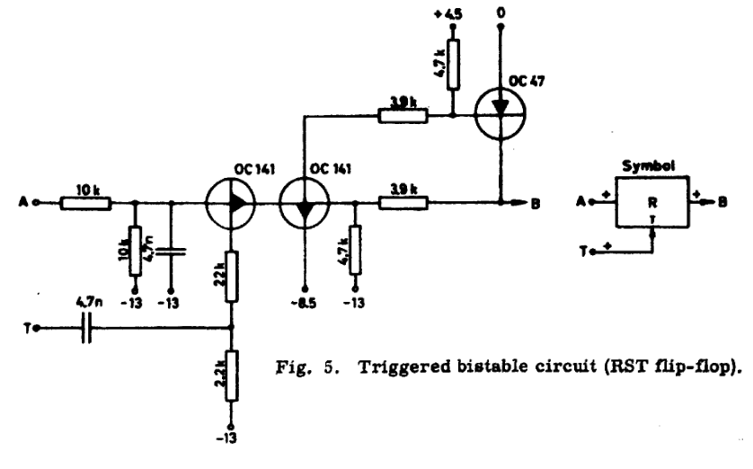
"Figure 5 shows the realization of a triggered bistable circuit with complementary transistors. The set-reset function is here performed by a symmetrical transistor;
if A is 0 volts (true value, "1"), the symmetrical transistor will work as an emitter follower and, by a pulse at its base, set the bistable circuit;
if A is not 0 volts (false value, "0"), the transistor will work as a collector follower and, by a pulse at its base, reset the circuit."
The latching cell contains a OC47 and OC141.
OC141 is NPN germanium, OC47 is PNP (like the OC70 I have).
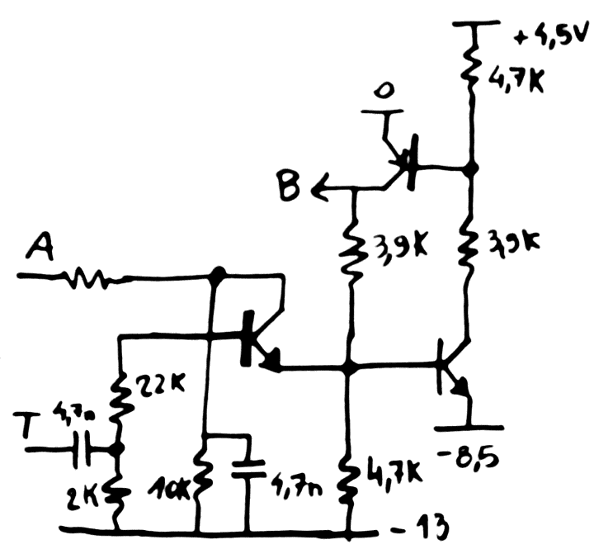
I am confused by the transistor symbols but I can try to reverse-engineer the circuit...
The right side is the latching part so the base loops to the collector of the other... How do I interpret the OC141 with 4 pins ? Well the right and left are probably the same node...
Creating a latch cell is pretty easy and does not depend on the polarity of the transistor so that's not critical.
What I'm after is a way to change/force the value with the least parts possible and the OC141 on the left does just that. This is the most interesting part !
Let's notice the two capacitors (of identical values: 4.7nF) and the resistor divider (10K, 10K) on the A input.
The capacitor on A stores the data's charge, while the series input resistor isolates it from the source circuit (probably to reduce data leakage while it changes from a simultaneous clock pulse).
The base is clearly (from the text) connected to the resistor divider 22K/2K, energised by the clock signal, through the series capacitor.
The point is clearly how they use a NPN to work as a "pass gate", while the input value is held in the capacitor. The clock capacitor has a similar value so both discharges are simultaneous.

Now, the awaken @esot.eric will notice that when A is low, B is high and a rising pulse appears on T, then the pass transistor is ... reverse biased ? Current will flow from B to the input capacitor (but not A because of the resistor).
Does that remind any Eric of a "almost functioning" circuit with a mistaken transistor ?
Whatever the case, it's very interesting because each DFF uses only 3 transistors, no diode (though I'll add one for the reset), and the circuit can be tuned for other voltage rails. It shouldn't be hard to modify it for an all-OC70 design.
With "only" 3 transistors, plus 2 to drive the outputs, the whole clock system requires something like 39DFF×5=195 transistors. Add some more for housekeeping (oscillator, buffers, drivers, decoders...) and this might reach 250 transistors, which is a desired outcome. The "pass trick" exposed above might be the detail that makes this whole project realistic.
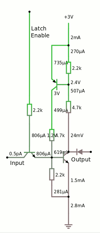
20200222 : I played more with Falstad and made the above circuit work for #Bipolar Discrete UART !

The input must be either floating (1) or grounded ( < 800 ohms) and the output has a diode to prevent any leakage that would override the current state (but can be ignored if a NPN base is driven through a 22K resistor for example)
 Yann Guidon / YGDES
Discussions
Become a Hackaday.io Member
Create an account to leave a comment. Already have an account? Log In.
erm, "the awaken esot.eric" is darn-near passing out, and somehow missed that bit when he was awake... was that an update?
Are you sure? yes | no
I have the habit of writing logs progressively and add/modify significantly, due to my old computer having an unstable/suicidal browser...
Anyway, it's interesting : has anybody tried to use a parallel pair of BJT but oe with swapped collector and emitter ? This would be a great pass gate !
Are you sure? yes | no
whew... this one's a bit above my head... but I think I see what you're saying. The low input to A and the high pulse from T causes that transistor to activate due to VCB's being forward-biased... that is, ignoring the rest of the circuit, which I can't quite wrap my head around.
One thing catching my attention is the second NPN, which I think would be active during T's positive-pulse, regardless of A and B... via normal means (VEB being positively-biased). But, again, that's ignoring the PNP... there's too much going on here for my brain!
FYI the "almost functioning circuit" was, in fact, "fully-functioning" per my needs, except that it was a buffer where I intended an inverter ;)
Interesting question re: parallel/swapped BJTs. The idea being e.g. a regular ol' NPN-inverter/"switch", where B is your input, C is your output (usually pulled up via resistor), and E is connected to ground...? Except, throw a second NPN with all its inputs directly connected to the first, (completely parallel) except with C and E swapped? Wonder what the effect would be. Would the swapped transistor's lower VCE force the non-swapped transistor to stay out of the saturation-region?
Are you sure? yes | no
I was more thinking of a pass gate, with Base=command pulse, C and E being data signal nodes.
C and E are swapped for the 2nd transistor for better symmetry.
It's only an hypothesis, "just a hack" and I've not seen it anywhere, because I just want to keep the parts count low (those 50's era transistors are not dirt cheap and I'll need a significant amount).
But if it works...
Anyway the "old/vintage" Ge transistors are full of drawbacks, like low hFE, high leakage, slow, significant capacitance... Fortunately the clock project requires rather "slow" circuits so I can make crazy compromises, like with the 10TFF :-D
Are you sure? yes | no
Ahh "pass-gate" ~= 4016/4066...? I see, then if they're parallel, it'll "pass" in both directions equally.
Are you sure? yes | no
Yes, years ago. I could never get it to work - but I was looking at analog signals. If you need to pass only a 0 or 1, maybe you can do it.
Are you sure? yes | no
@Ted Yapo: yes, but after reading @esot.eric's adventure, I see that it's possible to use a single transistor instead of 2 in reverse, however, i my case, the buffer cap should be larger (5× ?)
I'll try whenever my workshop is operational again.
Are you sure? yes | no
The transistor symbol alone is intriguing. I tried to find it used or explained anywhere else, without results so far. Does anybody know of some references?
Are you sure? yes | no
It's probably derived from internal looks of alloy-junction transistors, see below.
Are you sure? yes | no
Funny enough, the "normal" transistor symbol actually refers to old point-contact transistor arrangement, the "weird and old" from Yann's document refers to newer (though still fairly old) alloy transistor.
Are you sure? yes | no
Thanks, that's great! The "alternative" symbol looks much cooler (and it's faster to draw, too).
Are you sure? yes | no
Thanks Jaromir :-) That's what I suspected :-)
Are you sure? yes | no
LOL Those transistors are *weird* looking. Four ports?
Are you sure? yes | no
Old convention...
Only 3 pins but one side is "logically" connected to the other, to the base. Probably related to how transistors in the 50s were made (drift, diffusion, etc.)
I am trying to figure out which is the collector and emitter though but it will be deduced in the next minutes.
Are you sure? yes | no
Even WEIRDER are the voltages : -13V, -8.5V, 0V, 4.5V...
Are you sure? yes | no
This schematics symbol is not that weird, considering in 50's, most of them were alloy-junction transistors looking internally like this
the double base connection is relic from vacuum-tube days. Can't find an example, but I'm pretty sure I've seen schematics, where grid of simple triode was connected from both sides of schematics symbol, due to simpler "routing" of the schematics.
Could be worse, with capacitances in uuF or even in cm.
Are you sure? yes | no
Exactly, thanks for the external references :-)
Are you sure? yes | no