Yann Guidon / YGDES
-
Germanium is not for ever...
02/25/2020 at 19:35 • 2 commentsThe last log shows a preliminary shift register using 6 transistors per bit. For early Germanium technology this means that each complete clock would require about 100 PNP and 200 NPN.
PNP are now in stock but early "black glass" NPN are another story, a sad one : I just found that the stocks have now melted and the prices are increasing significantly ! I have just enough parts to test a few partial circuits...
If anyone can find affordable stock of OC139, OC140 or OC141 please contact me !
With the waning stock and perspective of suitable NPNs, I have to go back to the drawing board and finally design a bit cell that
- uses as few PNP as possible. Probably not 2 because the complexity is then pushed to more diodes and capacitors.
- dumps the concept of master-slave latches, to use fewer parts
I have met many problems with the classic flip-flop because of the metastabilities but I have two new insights and techniques to introduce :
- Adding a simple resistor at the middle of the cell (between both emitters and power) turns the FF into a "modified differential amplifier" and this could drastically reduce the metastabilities.
- I now understand better how a bipolar transistor could work as a "pass gate". This is a great trick to reduce the cell size because there would be only one point where data is forced into the FF, instead of 2 usually.
So there is still a chance to come up with something practical...
So let's start with a differential amplifier.
Here I have looped one branch to the other, to provide some feedback and hysteresis, this creates about 500mV of hysteresis @5V.
![]()
From there it is easy to loop the other "leg" back to the first and create a bistable circuit, except for the extra common resistor at the emitter. This will help in many ways, and hint Falstad at the much weaker metastability.
But it's still metastable : this sim initialises in "both conducting" state. There is some difference between the legs (360mV) but this is not enough to "flip hard".
![]()
The imbalance of the resistors should be higher then. But it doesn't solve the problem because then, the system is not bistable anymore...
I made a different change to manage the imbalance, by changing the gain :
![]()
the default value is 100 and a 10% variation is "normal". This helps the circuit become bistable again, even though it still initialises in metastable state...
Finally there is a different method to initialise the circuit with a well-defined state : the following circuit has a RC time delay on one branch so the imbalance occurs only during power-up. The transistors' gains don't matter much now.
![]()
It's still not a solution to the dynamic metastability problem but it opens another interesting prospect !
A whole block of latches can be reset directly by a complementary transistor that connects all the pull resistors. Previously I wanted to use a diode connected to the base of one of the transistors, but this diode would be connected to a common transistor. Here, I can avoid all the diodes, and the transistor can have the same rating, though it is ON all the time.
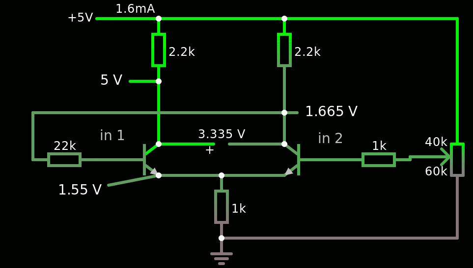
From there a more complete FF can be built :
![]()
It uses a single type/value of resistor, replicated by 6 : here I have chosen 8K2 because I just found a lot of vintage ones in my archives. It could be a bit different, depending on the power supply, speed and other details. Here the cell draws about 350µ @ 5V.
The power-on-reset cell (3 parts) is shared with all the other FF. The values will change and be tuned later.
The pass transistor is still the same here, but the trigger values vary considerably :
- The 1M resistor means that the transistor only needs one potential to polarise the component and select which way the base current will go. The whole base current is used to "upset" the base of the FlipFlop. A higher value than 8K2 on the base of the pass transistor would be possible if more current is available from the source. Though it woudn't work well for the other case :
- The 8K2 pull-down resistor is on the limit, because enough current must flow away from the FF base. The pass current then flows away, in the weakly amplifying direction
This 3-transistors, 6-resistors latch should be cascadable in theory, it uses only one kind of transistor and is minimalistic. But a fully clocked DFF requires 2 latches so it is not yet a solution...
The solution to the "latch duplication problem" would be in the sequencing of the latch strobes. I had considered a method, some years ago, and I'll have to refresh it... There would be as many phases to the clock as there are latches, so only one is transparent at a time. The temporary overlap is not a problem for the display part, but the sequencer must not use more than 2 transistors, 1 would be best.
And I must make sure the latch is cascadable.
Which is a tricky question because this circuit seems to let the pass transistor transmit a positive front transient... and I had to remove the emitter common resistors to have enough current to reset the slave.
This is solved with this circuit with a better protection against back-pulses on the supply rail. -
First shift register
02/09/2020 at 16:18 • 0 commentsOK I wonder how I'll manage to find complementary transistors... But you'all can agree it's a pretty awesome and minimalistic circuit !!!
![]()
The first great thing is there is a single clock line, though it must be driven by a push-pull circuit, with probably a complementary PNP-NPN pair.
The other great thing is that each slice uses 1×PNP and 1×NPN, plus either 1 PNP or NPN. So each bit uses 6 transistors, 4 diodes and 10 resistors. I can't see how to use fewer...
The main trick is to use "SCR-style" transparent latches, separated by either PNP or NPN "gates". This particular circuit uses the transistor is a very weird way, where the current flows in either the collector or the emitter, depending on the various voltages. So a single transistor serves in 3 cases : isolate, set or reset ! A couple of diodes is required however to prevent the right/destination from overwriting the left/source.
It would be possible (and possibly cheaper) to use only NPN pass gates with a system of complementary clock signals but the driving circuit is a whole different can of worms. The exercise is left to the implementer.
The source is getting crazy long... I wonder if all web browser will accept it. It's too long for the YT description though. I might upload the next circuits as files...
-----------------
Anyway I didn't find any weird or chaotic behaviour, as in the E&C circuit as before. The circuit would work at other supply voltages, with a little adaptation of the resistor values. You can notice the use of a single value : 2.2K :-)
This circuit is suitable for example for the UART project. The feedback with an inverted value adds another transistor so a divide-by-two is slightly more complicated and larger.
Anyway : the metastability issue is solved, the parts count is minimised and I can progress !
It's now a matter of how I can find complementary pairs in Ge... I have only 2 stocks of silicon complementary transistors : the Russian epitaxials, and the standard cheap BC549/BC550.
For single-type latches, I might have to study the system described by Ken Shirriff at http://www.righto.com/2017/07/inside-intels-first-product-3101-ram.html

Enjoy !
-
D-FF without metastability
02/08/2020 at 16:49 • 0 commentsExploring the First principles of Flip-Flops was very interesting but going back to the basic/classic "Eccles & Jordan" configuration (with 2× PNP or NPN) proved the weakness of the approach. The previous log I don't know why it works shows that metastability creates countless problems : it is very sensitive to initial conditions, operating conditions and parts values tolerances. I don't want to make a circuit that requires fine tuning and works only at a given frequency !
Metastability is when both transistors in the pair conduct. This is a third state of the flip-flop and under certain precise conditions, I would get a flip-flap-flop circuit, for who knows what reason. I tried my best to avoid the metastability but it's a systemic, fundamental flaw of this circuit and even adding parts, or using Ge transistors, the problem still lurks somewhere.
So I went back to some ideas from the earliest log From MUX to Latch and took a second look at the "SCR" approach. And this time I did it right :-)
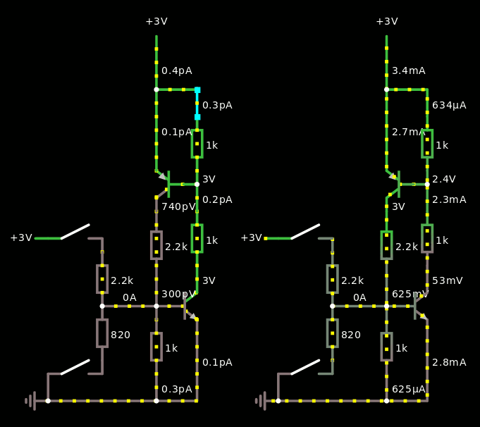
The basic SCR-latch has 4 resistors and 2 transistors. The only drawback is the complementary configuration : one PNP and one NPN... OTOH it doesn't suffer from the metastability plague and always powers up/initialises properly in "off" state !
![]()
The power draw is easy to control, by changing the resistors. I have put "no-brainer" values, with 1K the basic for medium currents. By default I choose 3V for the power supply, because I want to power it with a pair of AA batteries. A higher value has been used for the base NPN's pull-up so it is more sensitive to setting but it is not critical. The values will be adjusted for each application, with an appropriate compromise between speed and power consumption. Slower circuits will use higher resistors.
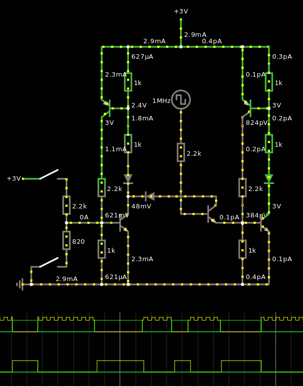
This circuits is reminiscent of the one discussed at 17. Another interesting BJT DFF circuit so I wanted to try the single-BJT circuit for transferring information from the last stage. Previously I used a different system, where I power the flip-flop selectively but I fear this wouldn't work at high enough speeds. However, a transistor can also be used in controlled ways as an almost bidirectional pass gate !
It is also reminiscent of the TTL gates input circuits, with the added trick that it is controlled by a signal, and not permanently pulled up by a resistor. And swapping the emitter and collector doesn't seem to make any difference.
In fact the BJT can be seen as a pair of diodes so the current from the base can go to the collector and/or the emitter (with more or less chance) IF the base is at a high enough potential. With some luck there is even some amplification :-)
Here the goal is to pull or push current through the base of the slave FF. The direction will depend on the potential of the "source" of current (the master). I found that I had to put a diode to prevent the slave from controlling the master FF...
![]()
Here is the link :-)
The latch is really transparent when the clock pulse is high so this is easily transformed into a DFF by adding the pass gate at the input of the M/s pair.
(full source in the description of the video)
Now is the time to turn it into a clock divider...
This circuit should it :
But I'm looking for a trick to perform the inversion, without the extra NPN...
Anyway, it's already good enough for a simple shift register :-)
In the last video, I saw that the 3.9K pull-up was not required. But that was not the end of it ! I'm now trying to design another system with 3 PNP and 3 NPN though it's very tricky but the potential savings are significant.
Now I wonder where/how I can find enough NPN in germanium... -
I don't know why it works
02/07/2020 at 21:52 • 3 commentsIt works as it should but I don't know why.
Here is the source code for Falstad :
$ 3 0.000001 0.34903429574618416 58 3 43
R 696 16 696 -16 0 0 40 4 0 0 0.5
w 808 352 808 384 1
w 808 192 808 176 0
w 584 176 584 192 0
w 664 96 592 96 3
w 808 288 808 256 0
w 728 176 808 176 0
w 384 64 384 136 3
w 696 112 696 176 1
w 584 176 664 176 2
w 584 288 584 320 0
w 584 256 584 288 0
w 664 288 584 288 3
w 808 320 808 288 0
w 728 288 808 288 3
w 672 336 728 288 0
w 720 336 664 288 1
r 808 256 808 192 0 1000
r 584 256 584 192 0 1000
t 616 336 584 336 0 1 0.5772267829335654 0.639069922813361 50
t 776 336 808 336 0 1 -1.1769217530853389 0.06184313995994596 50
g 808 384 808 416 0
g 584 376 584 416 0
w 696 16 696 32 1
w 696 32 696 80 0
t 664 96 696 96 0 1 -0.05293572317914741 0.6386489173065311 200
r 384 64 464 64 0 100000
w 496 80 496 96 0
t 464 64 496 64 0 -1 -0.5078879880313893 -0.5343748422129604 100
w 496 32 496 48 0
w 696 32 1160 32 0
r 496 96 592 96 0 1000
w 376 448 376 304 0
d 376 304 440 304 2 1N4148
d 376 256 456 288 2 1N4148
w 496 304 552 304 1
w 552 304 648 304 0
w 696 176 728 176 0
w 696 176 664 176 0
r 776 336 720 336 0 1000
r 672 336 616 336 0 1000
w 648 304 672 336 0
r 512 288 456 288 0 200
r 496 304 440 304 0 200
w 512 288 584 288 1
w 976 288 1048 288 1
r 960 304 904 304 0 200
r 976 288 920 288 0 200
w 1112 304 1136 336 0
r 1136 336 1080 336 0 1000
r 1240 336 1184 336 0 1000
w 1160 176 1128 176 0
w 1160 176 1192 176 0
w 1016 304 1112 304 0
w 960 304 1016 304 1
d 840 256 920 288 2 1N4148
d 840 304 904 304 2 1N4148
g 1048 384 1048 416 0
g 1272 384 1272 416 0
t 1240 336 1272 336 0 1 -0.5571041332660905 0.05744512506309504 50
t 1080 336 1048 336 0 1 0.5113871189769901 0.5688322439565177 50
r 1048 256 1048 192 0 1000
r 1272 256 1272 192 0 1000
w 1184 336 1128 288 0
w 1136 336 1192 288 0
w 1192 288 1272 288 3
w 1272 320 1272 288 0
w 1128 288 1048 288 3
w 1048 256 1048 288 0
w 1048 288 1048 320 0
w 1048 176 1128 176 2
w 1192 176 1272 176 0
w 1272 288 1272 256 0
w 1048 176 1048 192 0
w 1272 192 1272 176 0
w 1048 352 1048 384 1
w 1272 352 1272 384 1
w 1160 32 1160 80 0
t 1128 96 1160 96 0 1 -3.9999999998995 -0.3359971915536067 200
w 1128 96 1064 96 3
r 968 96 1064 96 0 1000
w 1160 112 1160 176 1
w 376 448 1112 448 0
w 384 136 968 136 0
w 968 136 968 96 0
w 664 288 704 256 0
w 840 256 704 256 0
w 808 288 840 304 0
w 1112 448 1184 336 0
w 1136 336 1160 472 0
w 1160 472 352 472 0
w 352 472 352 256 0
w 352 256 376 256 0
w 496 32 696 32 0
R 384 136 336 136 0 2 10000 2 2 0 0.5
w 584 352 584 376 1
o 94 2 0 4355 5 0.00009765625 0 2 94 3
o 14 2 0 4355 1.25 0.0015625 0 2 14 3
o 85 2 0 4355 1.25 0.0015625 0 2 85 3
o 53 2 0 4355 1.25 0.0015625 0 2 53 3
o 67 2 0 4355 1.25 0.003125 0 2 67 3
But when I change anything, it breaks... Worse, it can also create weird chaotic oscillations in some uncontrolled cases.
Metastability (when both transistors in a pair are ON) is a big problem as well... So I played with a capacitor to create some tiny imbalance but it was not the most efficient method.
-
More bistables...
02/03/2020 at 02:16 • 0 comments@jaromir.sukuba sent more more vintage germanium yummies and the cogs and wheels in my head resumed spinning again !
In the log From MUX to Latch, I started investigating other topologies for flip-flops and came up with a cell that was interesting but I wondered if it was optimal. After all the transistors have crawled upon the Earth for something like an eternity now and I've seen many circuits explored in the history, in this project...
The 2-transistor system has been extensively covered by this page and has always been lacking in a way or another. Slow, too many passive parts, tricky to setup... I want something with the fewest parts possible, stable, no capacitor and able to run fast. Even with lousy Ge trannies.
I was still not satisfied with the complex circuit I devised. The transistor count was ok but there are too many diodes for my taste. However the design of this flip-flop gave me more insights into what was good and what was to be avoided.
So I restarted back to the basics and used Falstad's online interactive simulator to build a cell from the basic principles ! And the result is quite unexpected...
![]()
It's really very basic ! All the resistors have the same value ! And I have avoided diodes ! You can run the sim with this code :
$ 1 0.000005 2.3728258192205156 60 5 43
g 128 352 128 384 0
g 336 352 336 384 0
t 304 336 336 336 0 1 0.5879810154813296 0.6224917671893107 200
t 160 336 128 336 0 1 -0.5879810154813296 0.03451075170798105 200
r 128 256 128 192 0 1000
r 336 256 336 192 0 1000
w 256 336 208 288 0
w 208 336 256 288 0
w 256 288 336 288 3
w 336 320 336 288 0
w 208 288 128 288 3
w 128 256 128 288 0
w 128 288 128 320 0
w 128 176 240 176 0
R 240 80 240 32 0 0 40 2 0 0 0.5
w 160 336 208 336 0
w 256 336 304 336 0
w 240 112 240 176 1
w 48 288 16 288 3
w 240 176 336 176 0
r 96 96 176 96 0 1000
r 48 288 128 288 0 1000
L 16 288 -16 288 0 1 false 0.63 0
L 96 96 64 96 0 1 false 2 0
w 336 288 336 256 0
w 208 96 176 96 3
t 208 96 240 96 0 1 -0.01041339040851752 0.6145396107402716 200
w 128 176 128 192 0
w 336 192 336 176 0
You can find the classic flip-flop with its two interlocked transistors, you can't make it more simple. I have chosen the version with only 2 resistors on the collectors, not the bases.
Then there is an emitter-follower that powers the flip-flop. The clock must go all the way up to the +Vcc rail but the driving current is nicely low, and decreases as the beta of the transistor increases. So a single PNP transistor could drive the main clock of a group. There is a 0.6V drop but it doesn't matter much. Swap it for a PNP if you prefer. It's interesting however because it insulates the pair of switching transistors from the supply, we'll see later why. The emitter follower can also be used to tune the supply voltage and current and more of these can be chained together.
So where does the data come from ? That's the whole trick in fact and it's not obvious... The principle/idea is :
- when the FF power is removed, the input data "bootstraps" the feedback loop.
- when the FF power is back on, it takes over and reinforces the loop, and makes the input data ineffective.
The solution I have found is apparently a simple resistor...
I still have some cases where the FF initialises with both transistors passing and I can't see why. Falstad can show some weird transient behaviours but something else is happening and I suppose SPICE would solve or resolve these patterns.
The resistor liaison seems to work almost well but relies on a very low input impedance behind the resistor, which might not be available, particularly in this circuit where I try to reduce the current as much as possible (because if it works, this circuit would be replicated tens of times !)
So I'm struggling to get a low impedance output and avoid forbidden states in the FF.
Anyway, 3 transistors and 3 resistors is a very promising circuit for a latch and I'll try to make it a full DFF !
The "bad starts" seem to be solved by taking the data input lower than the emitter of the nearby emitter. I don't want to add more rails and other crazy stuff but... I had the idea to "shift" the emitters with a resistor (it's also called "degeneration") and it seems to do wonders. The result has many advantages !
- quite low power
- all transistors are identical (can use either NPN or PNP)
- only 3 active devices
- enough margin for cascading into DFF and shift registers with direct connection
You'll notice that the LOW input level is 400mV and the HIGH input level is 900mV, inside the margin of the output swing (360mV-966mV).
This adds only 2 small resistors and we have the following ratios :
- 2R for the liaison resistor
- 1R for the pull-up resistors
- 1/4R for the degeneration at the legs
Only real implementation will tell if the speed it enough for my projects...
Here is the simulation of this new latch with Falstad :
And the source code :
$ 1 0.000005 2.3728258192205156 60 5 43
g 128 448 128 480 0
g 336 448 336 480 0
t 304 336 336 336 0 1 -0.5726792194301711 0.393378078449324 200
t 160 336 128 336 0 1 0.5726792194301711 0.6111078340910289 200
r 128 256 128 192 0 1000
r 336 256 336 192 0 1000
w 256 336 208 288 0
w 208 336 256 288 0
w 256 288 336 288 3
w 336 320 336 288 0
w 208 288 128 288 3
w 128 256 128 288 0
w 128 288 128 320 0
w 128 176 240 176 2
R 240 80 240 32 0 0 40 2 0 0 0.5
w 160 336 208 336 0
w 256 336 304 336 0
w 240 112 240 176 1
w 48 288 16 288 3
w 240 176 336 176 0
r 96 96 176 96 0 1000
r 48 288 128 288 0 2000
L 16 288 -16 288 0 0 false 0.9 0.4
L 96 96 64 96 0 1 false 2 0
w 336 288 336 256 0
w 208 96 176 96 3
t 208 96 240 96 0 1 -0.0070514786969611 0.6044560065624918 200
w 128 176 128 192 0
w 336 192 336 176 0
r 336 448 336 384 0 250
r 128 448 128 384 0 250
w 128 352 128 384 3
w 336 352 336 384 3
From there on, it should be easy to create a shift register...
Well, it was not as easy as I thought ! And Falstad gives me a lot of troubles with weird simulations that seem random and give results that vary from one run to the other. I had to add capacitors to stabilise some things...
The good sides are : it uses fewer parts and draws less current (about 3mA with these parameters). Only 2 diodes have been added for the liaison, which is a pretty neat and cheap compromise.
![]()
Here is thesource code for the sim :
$ 1 0.000005 0.13386567243530942 58 5 43
g 128 448 128 480 0
g 336 464 336 480 0
t 304 336 336 336 0 1 -0.5841634814225252 0.4903224664076705 50
t 160 336 128 336 0 1 0.5841634814225252 0.6209564153103788 50
r 128 256 128 192 0 1000
r 336 256 336 192 0 1000
w 256 336 208 288 0
w 208 336 256 288 0
w 256 288 336 288 3
w 336 320 336 288 0
w 128 256 128 288 0
w 128 288 128 320 0
w 128 176 240 176 2
R 240 32 240 0 0 0 40 3 0 0 0.5
w 160 336 208 336 0
w 256 336 304 336 0
w 240 128 240 176 1
w 48 288 16 288 3
w 240 176 336 176 0
r 96 112 176 112 0 1000
r 48 288 128 288 0 2000
L 16 288 -16 288 0 0 false 1.2 0
L 96 112 64 112 0 1 false 3 0
w 336 288 336 272 0
w 208 112 176 112 3
t 208 112 240 112 0 1 -0.01565201462221122 0.6250797824248919 200
w 128 176 128 192 0
w 336 192 336 176 0
r 336 448 336 384 0 220
r 128 448 128 384 0 220
w 128 352 128 384 3
w 736 352 736 384 3
w 528 352 528 384 3
r 528 448 528 384 0 220
r 736 448 736 384 0 220
w 736 192 736 176 0
w 528 176 528 192 0
w 608 112 528 112 3
w 736 288 736 256 0
w 656 176 736 176 0
w 304 80 96 80 3
w 640 128 640 176 1
w 656 336 704 336 0
w 528 176 608 176 2
w 528 288 528 320 0
w 528 256 528 288 0
w 608 288 528 288 3
w 736 320 736 288 0
w 656 288 736 288 3
w 608 336 656 288 0
w 656 336 608 288 0
r 736 256 736 192 0 1000
r 528 256 528 192 0 1000
t 560 336 528 336 0 1 0.5612474813757181 0.5967515964862364 50
t 704 336 736 336 0 1 -0.5612474813757181 0.21207598906918554 50
g 736 448 736 480 0
g 528 448 528 480 0
w 240 32 240 48 1
w 240 48 240 96 0
w 240 48 288 48 0
w 640 48 640 96 0
w 96 80 96 112 0
t 608 112 640 112 0 1 -2.3418004906459884 0.1654996677481867 200
r 304 80 384 80 0 100000
w 416 48 528 48 0
w 416 96 416 112 0
t 384 80 416 80 0 -1 2.3418004804459738 -1.0000014594169215e-8 100
w 416 48 416 64 0
w 528 48 640 48 0
r 416 112 528 112 0 1000
w 336 384 336 352 2
w 336 464 336 448 1
w 208 288 128 288 3
w 336 256 336 272 0
w 496 288 528 288 0
w 288 48 416 48 0
w 560 336 608 336 0
w 464 288 496 288 1
d 400 304 464 304 2 1N4148
d 400 256 464 288 2 1N4148
w 464 304 512 304 1
w 512 304 576 304 0
w 656 256 656 288 0
w 400 256 240 256 0
w 240 256 208 288 0
w 640 176 656 176 0
w 640 176 608 176 0
w 608 336 576 304 0
c 656 256 656 176 0 1e-9 0.28062371048784684
c 608 288 608 176 0 1e-9 -0.28062377088787127
w 336 288 400 304 0
x 558 210 668 213 4 14 1nf\sfor\ssim\sonly
38 22 2 0 3 CLK\slow
38 22 1 0 3 Clk\sHigh
38 21 2 0 3 Din\sLow
38 21 1 0 3 Din\sHigh
And a little video...
It is obviously still flawed but we're almost getting there ;-)
...
-
Even more bistables: plot twist !
10/17/2017 at 12:10 • 2 commentsToday I received an email that I couldn't expect at all. Enjoy !
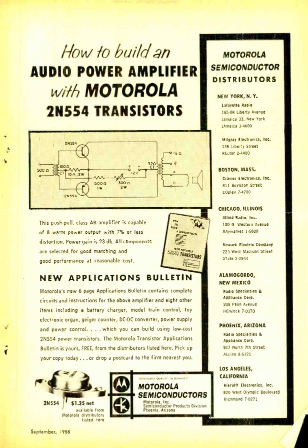
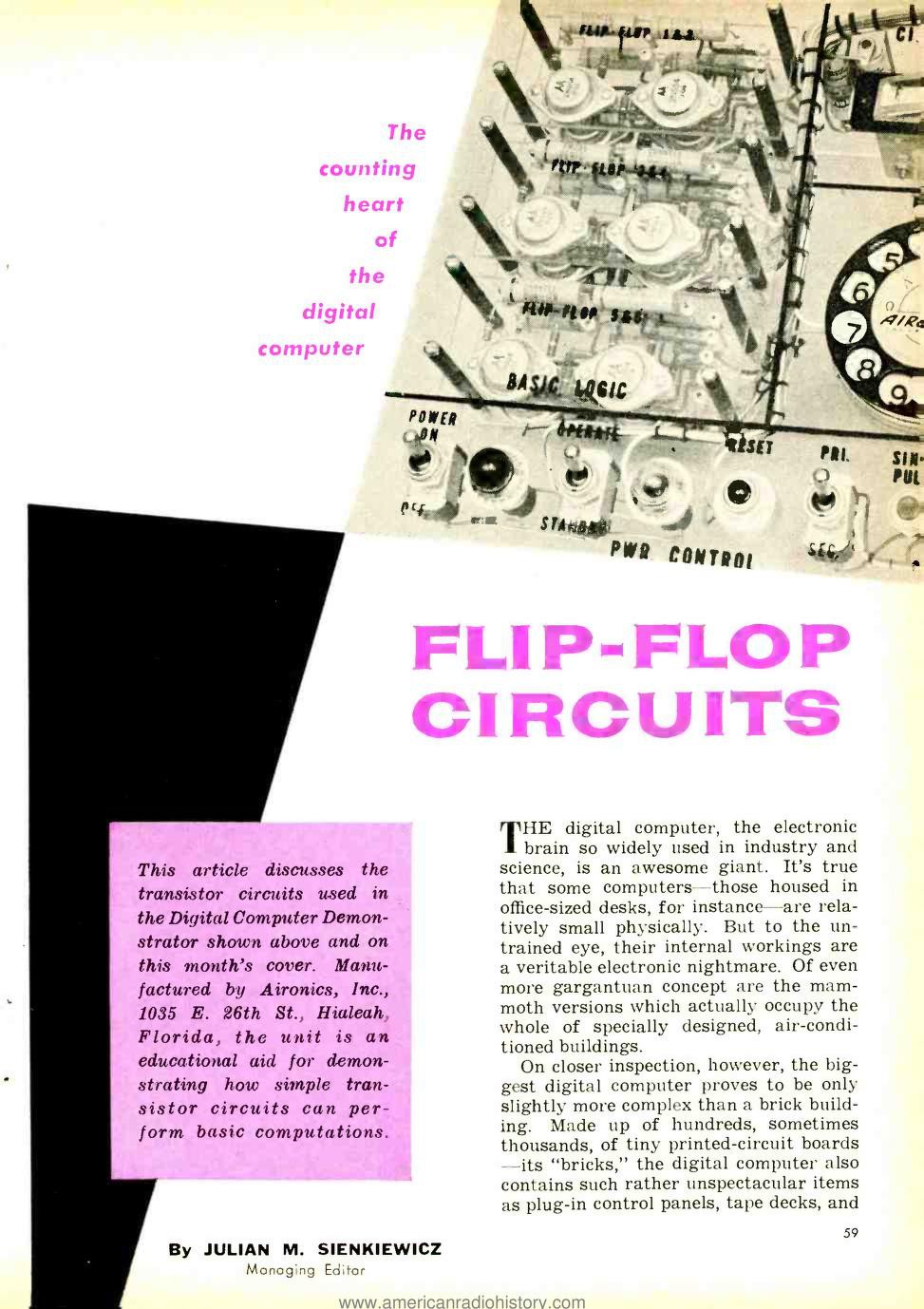
I enjoyed your hackaday posting of the 2n554 flip-flop circuit. I built the computer described in that Popular Electronics article in high-school in 1964. Those circuits were later reused in my KB/67 (Kalin-Burkhart) project.
Here's a bit more about the history of that flip-flop circuit. I was always curious where that circuit design originated, and did some follow-up. That flip-flop was also featured in the January 1960 issue (page 65) of Electronics Illustrated in an article by Ronald Benrey. He contributed many projects to electronics magazines during that time. His homemade satellite appeared in the October 1958 issue of Popular Electronics.Looks like the flip-flop circuit is from Performance Tested Transistor Circuits, (page 47) published by Sylvania in 1958. Although that circuit uses a different transistor, 2n307, Benrey substituted the 2n554, which was a common substitution.
Before finding the Sylvania document, I thought perhaps that the circuit may have come from a Motorola publication.There was a 2n554 application bulletin published, which I've not been able to find. But I did find an ad (attached) for that bulletin. At least from that write-up, the flip-flop circuit is not included.
![]()
(7% distorsion, yay !)
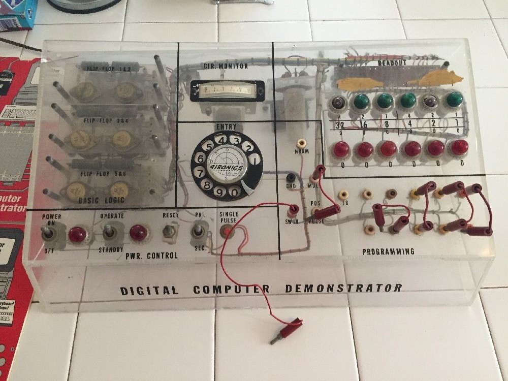
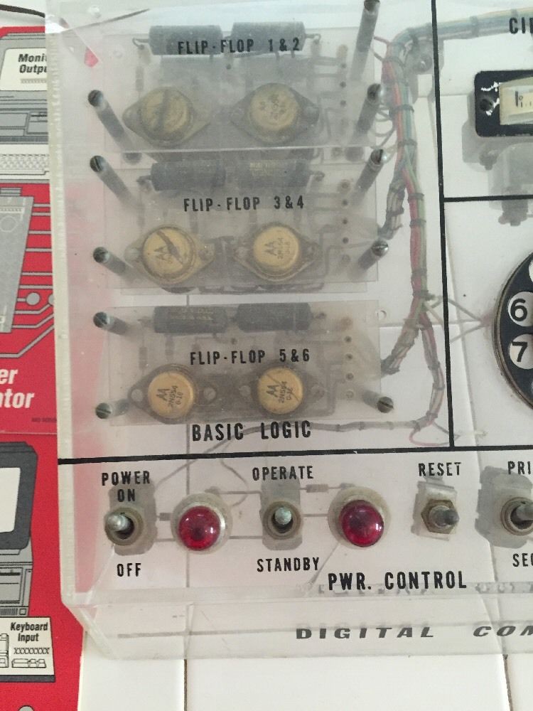
That demo computer described in the PE article also made the cover of Computers and Automation in Nov 1960.
Very brief description on page 20. One of these units was listed on ebay last year, 2 photos attached.![]()
![]()
How awesome is that ?
-
Even more bistables !
02/04/2017 at 22:40 • 16 commentsThe last log (More bistables) found some explanations of the weird flip-flop schematic I initially found.
Today, a comment by RSMilward on hackaday.io brought a new light to the mystery !
This one comes from an even earlier publication (1961) in Popular Electronics, hosted on archive.org :
![]()
![]()
![]()
![]()
![]()
From the experience with the 10TFF and looking at vintage circuits, I realise something about edge-triggered flip-flops with only 2 transistors. In the 10TFF, a temporary value is held as a charge on one transistor's gate. This principle is found in the 2BJT circuits with actual capacitors, which are "protected" from the previous stage by a series resistors.
This resistor is critical for the speed and power consumption. The RC constant must be adapted to the system's speed. That's where the 2BJT circuits reach their limit... For the "slow" parts of the clock, this is not a problem and this will save quite a lot of germanium parts, but there are quite a few diodes and other passive parts.
-
More bistables
01/18/2017 at 23:46 • 0 commentsI still feel that the divide-by-two diagram in the "details" page is messy.
I tried to address this (rather critical) issue in Easier frequency division but the principle is not reliable enough.
I just stumbled on a better laid out circuit at http://www.smrcc.org.uk/members/g4ugm/Manuals/wirelessworldcomputer.pdf
![]()
The old (1968?) book also explains how the whole thing works.
I faintly remember seeing this sort of circuit in one of @Shaos's russian books but 1) I don't read russian 2) the circuit was pretty messy too...
I'm concerned that the OC70 might not be fast enough to work at 18KHz so I must find a more reliable (ECL-based ?) method for the first stages of the predivider.
I'm puzzled by the circuits of that time : they use 3 power rails (-Vcc, 0V and +Vcc). +Vcc seems to be used only as a "pull-up", maybe to accelerate charge dissipation and recover from saturation. I'll have to substitute with Germanium diodes for Baker clamps...
Now, considering that a ECL latch uses about 7 transistors (a DFF uses 14), the predivider would be too expensive with this approach. However, the circuits close to the resonator will work close to the maximum speed of the transistors...
-
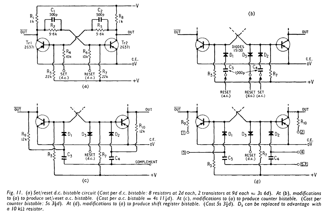
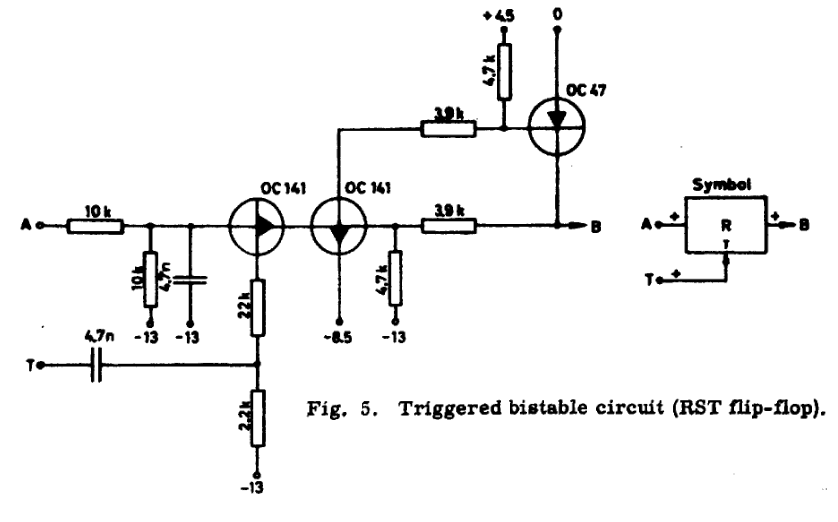
Another interesting BJT DFF circuit
01/09/2017 at 03:25 • 17 comments20200222 : see update at the bottom
I've been pretty confused by the 2-transistors latch that is shown on the project details page. I've been looking of a simpler, yet compact DFF circuit that uses few transistors.
Today I've done some research on the subject of #CBJT Logic and I came across this PDF : http://orbit.dtu.dk/fedora/objects/orbit:91667/datastreams/file_0b85d918-7d44-40c2-b7c7-a4332b0ce2b6/content
![]()
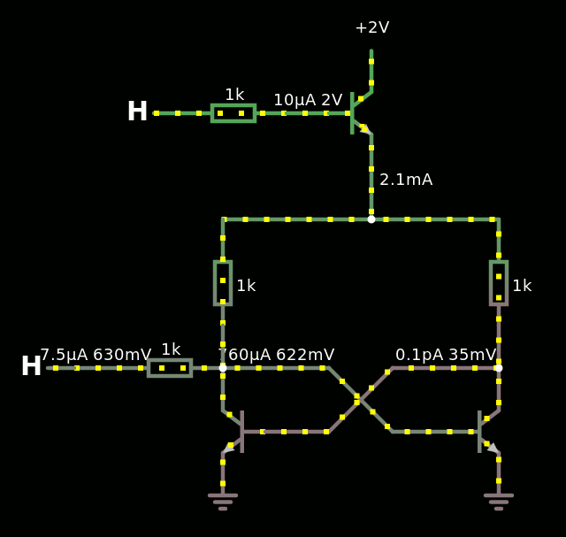
"Figure 5 shows the realization of a triggered bistable circuit with complementary transistors. The set-reset function is here performed by a symmetrical transistor;
if A is 0 volts (true value, "1"), the symmetrical transistor will work as an emitter follower and, by a pulse at its base, set the bistable circuit;
if A is not 0 volts (false value, "0"), the transistor will work as a collector follower and, by a pulse at its base, reset the circuit."
The latching cell contains a OC47 and OC141.
OC141 is NPN germanium, OC47 is PNP (like the OC70 I have).
I am confused by the transistor symbols but I can try to reverse-engineer the circuit...
The right side is the latching part so the base loops to the collector of the other... How do I interpret the OC141 with 4 pins ? Well the right and left are probably the same node...
Creating a latch cell is pretty easy and does not depend on the polarity of the transistor so that's not critical.
What I'm after is a way to change/force the value with the least parts possible and the OC141 on the left does just that. This is the most interesting part !
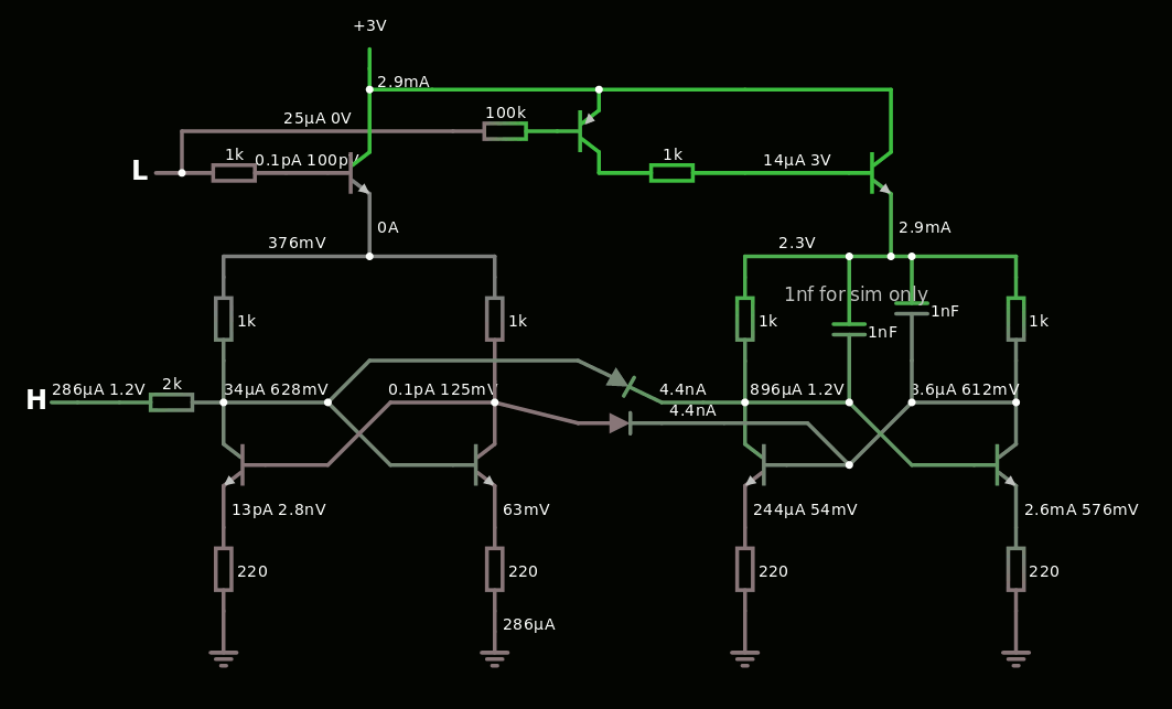
Let's notice the two capacitors (of identical values: 4.7nF) and the resistor divider (10K, 10K) on the A input.
The capacitor on A stores the data's charge, while the series input resistor isolates it from the source circuit (probably to reduce data leakage while it changes from a simultaneous clock pulse).
The base is clearly (from the text) connected to the resistor divider 22K/2K, energised by the clock signal, through the series capacitor.
The point is clearly how they use a NPN to work as a "pass gate", while the input value is held in the capacitor. The clock capacitor has a similar value so both discharges are simultaneous.
![]()
Now, the awaken @esot.eric will notice that when A is low, B is high and a rising pulse appears on T, then the pass transistor is ... reverse biased ? Current will flow from B to the input capacitor (but not A because of the resistor).
Does that remind any Eric of a "almost functioning" circuit with a mistaken transistor ?
Whatever the case, it's very interesting because each DFF uses only 3 transistors, no diode (though I'll add one for the reset), and the circuit can be tuned for other voltage rails. It shouldn't be hard to modify it for an all-OC70 design.
With "only" 3 transistors, plus 2 to drive the outputs, the whole clock system requires something like 39DFF×5=195 transistors. Add some more for housekeeping (oscillator, buffers, drivers, decoders...) and this might reach 250 transistors, which is a desired outcome. The "pass trick" exposed above might be the detail that makes this whole project realistic.
20200222 : I played more with Falstad and made the above circuit work for #Bipolar Discrete UART !![]()
The input must be either floating (1) or grounded ( < 800 ohms) and the output has a diode to prevent any leakage that would override the current state (but can be ignored if a NPN base is driven through a 22K resistor for example)
-
Easier frequency division
05/23/2016 at 04:10 • 0 commentsThe OC70 is a "lazy" transistor and the 8KHz oscillator is close to its maximum working frequency. Yet this frequency must be divided because the digital counters need "time" to work. I've been naturally thinking of an analog circuit that oscillates at 1/2 or 1/3 of the input frequency, and gets synchronised to the input frequency, which would be the reverse of an "overtone" frequency multiplier.
Well this idea has been studied for a century already, as mentioned in http://www.leapsecond.com/pages/marrison/
"
This procedure was reversed by Hull and Clapp72, who discovered that the fundamental frequency could be controlled by coupling the high-frequency source directly into the circuit of the multivibrator. This, in fact, is a general property of any oscillator in which the operating cycle involves a non-linear current-voltage characteristic, being most pronounced in those of the relaxation type. Van der Pol and Van der Mark in 1927 reported on some experiments on "frequency demultiplication" using gas tube relaxation oscillators73. The multivibrator is, in effect, a relatively stable relaxation oscillator74, and with slight modification has been used extensively as the frequency-reducing element in quartz-controlled time and frequency standards throughout the world.
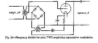
One serious difficulty with the multivibrator type of submultiple generator has been that, if the input fails or falls below a critical level, it will continue to deliver an output which, of course, will not hen have the expected frequency. Certain variables in the circuit, such as tube aging, may cause a similar result. With this in view, a general method for frequency conversion has been developed by R. L. Miller75, in which the existence of an output depends directly on the presence of the control input. The basic, idea involved in this, now known as regenerative modulation, was anticipated by J. W. Horton in 191976 but had not been developed prior to Miller's investigations. The circuit of a regenerative modulator in its simplest form as a frequency divider of ratio "two" is shown in Fig. 12.
![]()
Fig. 12--Frequency divider for ratio TWO employing regenerative modulation."
So once again, reinventing the clock with old parts lets me discover century-old methods. I have seen a few relaxation oscillators used as frequency dividers and they look more practical than flip-flops, can run faster and use less parts.
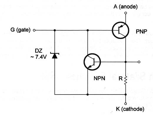
It is possible to do a relaxation oscillator by combining a PNP and NPN transistor to create a SCR such as the "SUS" 2N4989:
![]()
So it was a very fortunate idea that I got some OC139 (NPN Ge) !
For the Zener, a LED will also work, I suppose ;-)
The other benefit of a relaxation oscillator is the possible cross-coupling with the Xtal oscillator to "help" or "kick" it into oscillation.
My initial idea was more using an astable multivibrator. In fact that's what Injection-Locked Frequency Dividers (ILFD, discovered at Crystal oscillator with MOSFETs (new episode)) do, by modulating the operating voltage of the multivibrator with another transistor. The advantage of a multivibrator is that it uses only one kind of transistors so it will not use my short supply of 0C139.
Clockwork germanium
A retro version of Yet Another (Discrete) Clock, with vintage parts