Yann Guidon / YGDES
-
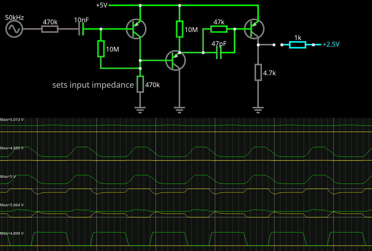
Clock preamp 3T
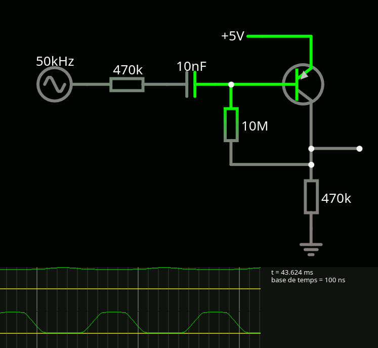
08/25/2023 at 22:28 • 9 commentsThis circuit seems to work well in simulation, provided you let the first input stage settle for a while, as it charges the 10nF coupling cap.

We have seen the first stage in a previous log so no need to repeat it : it uses the coupling cap as a reservoir too, so it takes a while for the bias to get "right" through the 10M resistor. On its own, it can amplify quite a bit, at least in amplitude. But the output drops as soon as some load is tied.
Then an emitter follower "buffers" the output. It acts almost as a Darlington pair with the 3rd but there are impedance issues so a RC network makes the junction.
Then a final stage does the saturated voltage amplification to get cleaner edges and a decent rise/fall time.
All transistors are set as hFE=20. Notice the various resistors : 470K, 47K then 4.7K, reducing impedance by 10x at each step.
The 10M pull-up has a strange behaviour in the simulation, as it raises the 3rd transistor's base above 5V, sometimes 6.5V depending on the capacitor and other factors. 47pF is "mostly harmless" but really helps with the output rise times.
The output signal drops when a load is tied, and I want to have even lower output impedance to drive 2 clock signals.
Of course the same usual limitations apply !
- The transistor of the simulation is not a Germanium type
- Leakage is not taken into account
- Baker capacitances are not considered either
So there will be quite a lot of differences but the simulation helped me understand the role of each part's value.
-
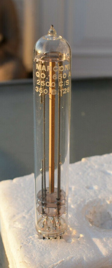
Inside OC70
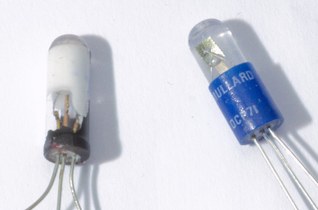
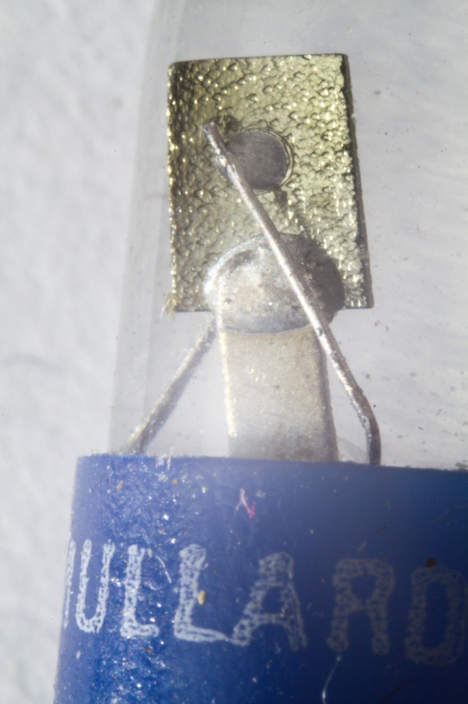
08/23/2023 at 21:35 • 3 commentsI have a few OC70 (or so it seems, as there is no marking).
But it's not easy to look inside the glass casing, because it is filled with a silicon grease mixed with opaque alumina powder... to prevent people from scratching the cellulose black paint and use it as a phototransistor. This had to be done with a OCP71, the very same thing but sold 3× the price, because the sikicone grease is clear.
This is shown in the pictures below :
The left shows the stock OC70 with some black paint scratched, and the right is the OCP71. We can only infer that the insides are identical. So let's zoom inside the OCP71 :
It's an "alloy" transistor where the doped germanium chip is tied to the base (the large electrode), and the emitter and collector are tied through another metal (usually indium) "alloyed" by fusion in a oven.
These transistors are not the fastest, on the contrary, but much better than the early point-contact models. They have decent audio performance and enhanced versions could reach some tens of MHz. But here, it's an audio-range device. Hopefully it can reach the speed of the quartz resonators :-)
-
Funny clock preamp
08/23/2023 at 17:47 • 4 commentsThe signal generated by the crystal oscillators are, to say the least, weak and any influence (real or reactive) downstream will affect the resonator upstream. So the project has been blocked for years, among others, by the requirement of a very high input impedance amplifier. I have looked at differential amplifiers but it's pretty complex. If possible, it should be simple, right ? Well I have found one solution !
Two high-value resistors, one cap and one transistor, can you do better ? Here is the sim !
It is pretty neat and I simulated the high impendance with the 470K series resistor, just to prove the point. The series capacitor also helps separate the levels but there are many things to consider though.
First : it takes "a while" to start up when fed with an appropriate signal. In the sim, it takes about 30ms to stabilise. This is because it uses a silly trick : the series capacitor must also "charge" to the right level and it takes a while, through the 470K ground resistor. But once is starts to conduct, the 10M feedback resistor keeps the average base level at approximately the conduction level. The duty cycle is controlled by the value of the grounded resistor, 470K seemed to work BUT this resistor also affects the input impedance !
Second : I used a "near perfect" Silicon PNP model. Germanium will leak and spit noise, they drift with temperature, the bandwidth is not great... So the values might change and equilibrium is not certain, but the rough order of magnitude is here.
Anyway the circuit
- is pretty sensitive (I used a 1V input amplitude but it can be lower)
- sips very little current, since the 470K passes 11µA max (10× less than leakage)
- uses few parts
- is easy to tune (the ground resistor might be adjustable and that's it)
- amplifies greatly even when I limit hFE to 20
- saturates nicely...
Further amplification stages are required, the lower the hFE the more stages.
And now I realise it is very similar to one part of the circuit in log Crystal Oscillator (Germanium Edition). Except that this branch will drive a high-gain amplifier (then a current buffer), not a resonator.
We'll see how it translates in practice. -
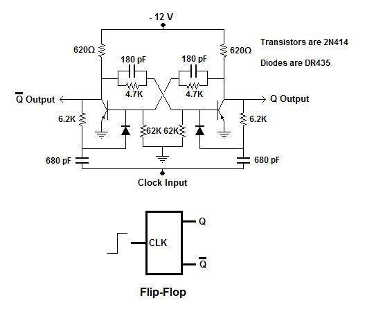
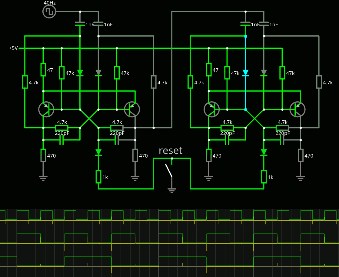
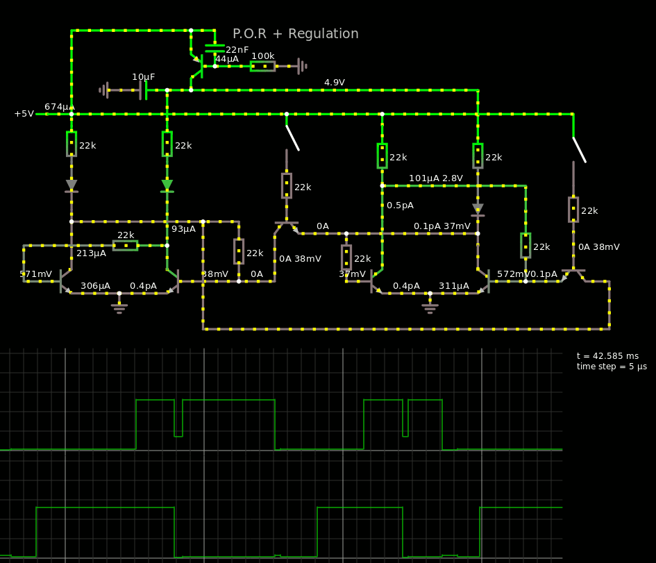
Working bistable at last !
08/23/2023 at 00:50 • 6 commentsI was hanging out on a Facebook group dedicated to Minimalist computing (which is perfectly in line with the #YGREC8 project) and a retired engineer dropped a little schematic.
Joseph Watson posted a circuit I have seen again and again, and consistently failed to make work : the venerable symmetrical bistable.
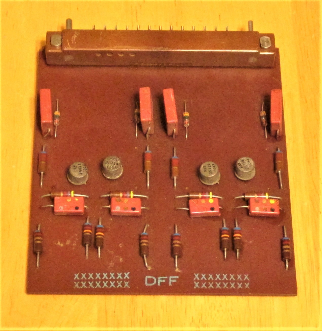
But this time with parts values !!! And this is a working circuit, as proved by his pictures of the circuit boards for his homemade computer built in the 60s.
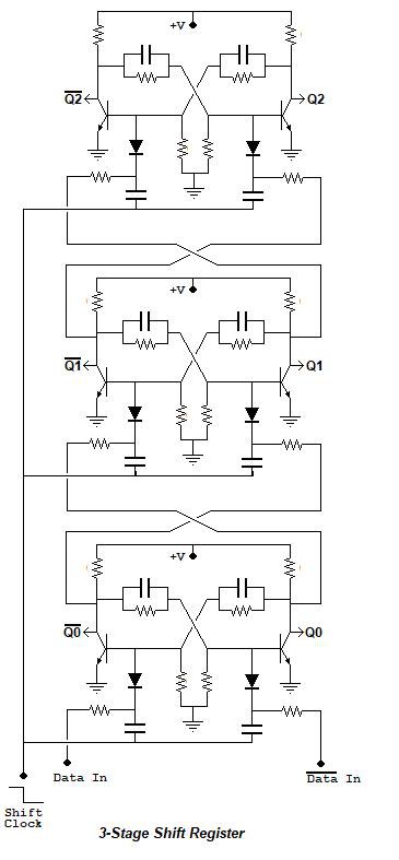
This circuit can be easily reconfigured from divider-by-two to shift register :
As we already know, this 3-stage Shift Register can be easily looped back on itself with one inversion (swap the positive and negative signals at one point) to make a 6-step Johnson counter. Which is exactly what a digital clock needs (for the decimal digit, and the unit digit needs 5 bistables) !!!
So what are the issues ?
- First, I've always had troubles simulating this circuit with CircuitJS. Well, I made my own version of the above circuit (which does not differ from many other versions I have seen before) and this one works (when you get the diodes in the right polarity!).
I rounded the parts values to E3 and it passes the simulator, however it must be "bootstrapped" because it insists on initialising in a "stuck" state. That will be the job of a master reset ciruit.
- Second : Germanium drifts to Vbe=0.2 or 0.1 when the temperature rises. Which makes this type of grounded-emitter circuit difficult to operate. The parallel capacitors on the bases might help solve this issue but I have considered adding a diode on the ground side to "shift" the level. The VceSat might not bring the base down to the desired value to stick the circuit to the new desired state. Maybe a degenerating resistor and/or a diffpair-like topology could help too.
- Third : Speed. The RC constants might in fact slow the whole circuit down, but there is no choice because it's the only minimal circuit with identical transistor polarities. To get to 100KHz, a careful design is required : trying and choosing the appropriate resistors and capacitors... Not too large, not too small..
- Signal voltage swings are not characterised (over Vcc and temperature) and this will be another challenge. Here again, the capacitors will help, but also impede the frequency...
So this circuit brings in quite a lot of "analog design" but we can start from the transistors themselves : the above 2N414 are not far from the OC70 : they both are alloy junctions.
Some specs of the 2N414 : 3MHz, 24pF, hFE>60, 15V, 200mA, 200mW
The OC70 is more modest and I'll tune all my circuits for 10mA Ic and 1mA Ib to be more consistent with other, speedier references (because I want to use AF240 later).
From these values, one can deduce several values, and I'll keep the Vcc at 5V (because). So to get about 10mA at 5V, that's a 470 ohms resistor for the collector.
The Ib is 1/10th of the Ic so the base resistors are 470*10=4K7. Awesome.
There is a pull-down resistor for the base, that
- keeps the base at a low value when OFF, though it might not be low enough and the 10× value might slow down the off-turning. This is where "shifting" the emitter could be useful, as it would provide the pull-off resistor some headroom to totally discharge the base.
- limits the voltage on the base : 5V is applied to the base through 470+4K7 (that's 5K overall) but the 47K prevents the voltage from exceeding about 0.5V (in continuous operation). At 0.5V, the transistor can be considered "fully on"...
I'll have to check degenerating resistors, either individual of common, to keep the circuit from saturating too much. Using 100K instead of 47K for the pull-off resistors would be OK with 0.5V of degeneration, which means 47 ohms... Aaaannnnnnd this makes the circuit unstable... It's solved with a common resistor though.
There is another problem that the simulator does not let me estimate : the effect of the leakage currents ! 100µA here, 200µA there, and the whole balance might be shattered...
Yet another problem is that the transistor model is a standard silicon type with Vbe=0.6V so the values that work might not be right for germanium.
One more problem ! The clock signal must have a large swing : at least 4V for 5Vcc, as the simulation destabilises otherwise.
Anyway I have one version that seems to cascade decently :
...
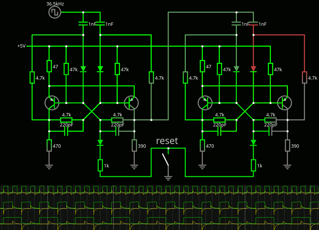
I solved the init and another stability problem by reducing one of the resistors, from 470 to 390, this takes the circuit out of equilibrium and back to clear binary state. I seem to be able to simulate easily up to 36KHz with the above caps, I doubted that the 1nF could charge fast enough through the 4K7 feedback resistors...
Now this does not account for 1) lazy transistors 2) leakages 3) Vbe.
But at least I could validate a clock buffer using an emitter follower.
-
More Germanium lemonade, OC70 edition
07/11/2023 at 00:07 • 0 commentsThe log 29. Germanium lemonade covered the OC139 in my stock. I only have 70pcs of this NPN type, but I have significant reserve of the PNP type and it's time to break the suspense. Let's bin some !
n° hFE Vbe mV Ic mA Ice0 mA Ices µA 1 47 212 6.4 0.13 7 2 35 199 6.6 0,23 25 3 26 214 6.6 0.35 44 4 27 95 0.5 0.2 23 5 30 213 6.6 0.33 40 6 25 210 6.6 0.26 32 7 39 194 6.7 0.2 19 8 19 220 6.5 0.31 30 9 34 207 6.6 0.35 35 10 28 213 6.6 0.23 33 11 22 222 6.5 0.20 25 12 21 239 6.5 0.12 18 13 26 223 6.6 0.28 47 14 34 194 6.6 0.25 31 15 30 104 0.7 ? 0.37 31 16 35 95 0.81 0.44 52 17 32 220 6.6 0.37 40 18 34 97 0.64 0.30 35 19 32 211 6.6 0.4 45 20 45 107 0.8 0.35 30 21 34 195 6.6 0.23 30 22 42 204 6.7 0.25 20 23 33 102 0.71 0.36 35 24 37 196 6.7 0.35 46 25 23 220 6.5 0.33 45 26 35 193 6.6 0.31 31 27 37 203 6.6 0.31 30 28 29 199 6.6 0.37 49 29 29 212 6.6 0.35 41 30 32 94 0.75 0.41 48 31 30 103 0.77 0.45 45 32 31 98 /200 0.57 / 6.6 0.25 /0.16 14 33 25 92 0.48 0.22 32 34 26 210 6.6 0.33 44 35 26 200 6.6 0.29 30 36 28 210 6.6 0.44 45 37 31 203 6.6 0.40 52 38 27 88 0.61 0.32 41 39 29 93 0.70 0.45 62 40 25 218 6.5 0.34 54 41 41 110 / 210 0.73 .26 20 42 32 230 6.6 .39 49 43 20 224 6.5 .32 59 44 29 207 6.6 .19 18 45 44 102 0.89 .43 41 46 34 197 6.6 .24 29 47 33 187 6.6 0.25 28 48 34 207 6.6 0.23 24 49 34 216 6.6 0.29 34 50 46 103 0.70 .22 18 51 23 209 6.5 .39 54 52 25 229 6.5 .22 32 53 32 193 6.6 20 31 54 29 210 6.6 .38 48 55 25 98 0.74 0.37 44 56 47 108 1.0 0.5 35 57 28 225 6.6 0.25 32 58 38 198 6.7 0.37 37 59 26 206 6.6 0.36 57 60 44 190 6.7 .35 34 There is this grouping of Ic at 6.6mA and then a few around 0.6mA, which corresponds to Vbe around 0.1V. So maybe this is a batch of mixed bins. However items #32 and 41 measurements show that the values vary randomly so maybe it's it's the tester...
hFE is at least 20, sometimes more than 40. there is not much apparent correlation with Vbe. Remember that these values vary with temperature and it's now 27°C (ambient). The Ice0 and Ices seem somewhat proportional, the have a 50% variability between consecutive tests but it's in the same ballpark.
Overall, despite the quite low Vbe, it's a good batch and not a bad lemonade. Maybe the rumor is true, these are recently made OC70s from a new factory ?
Now the other question is : how fast does that tranny switch ?
-
More inspiration
01/20/2021 at 01:56 • 0 commentsAs mentioned in #Bipolar Discrete UART I am in awe when watching this fabulous build :
The most interesting part is at 15:50 and I have examined and even simulated this circuit at An even better SCR-based sequencer. This is an impressive design that inspires me again because I want to turn it into a Johnson counter, which is a special case of shift register, which is also something needed for the #Bipolar Discrete UART ...
The name of the game is minimalism ! As noted before in 25. Germanium is not for ever..., the number of available vintage parts has dramatically shrunk and their price has exploded, so the fewer parts, the better !
The design that Leo chose has 1P1N per count: that's 20 transistors per digit, where a Johnson counter would use only 1P1N×5=10 total, which would use only 48 transistors for H:M:S.
Transforming the SCR latch sequencer into a shift register is not trivial but it should be possible. This would be also a great thing for the UART, because there would be no "slave latch". Looking at the schematic/diagram, which looks like a transistorized Dekatron, the clock pulse is driving ALL SCR through one shared diode, and "current steering" (something similar to the effect of a differential pair) will send the most current to one of the branches, which is pre-selected by the charge of a capacitor.
This is this individual branch that must be tweaked, adapted, transformed, so it behaves like a D-flip-flop. Then it will be useful for a wide range of circuits :-)
I know I should look more carefully at the works on the Shockley diode. More early SCR research can be found at https://www.rfcafe.com/references/electronics-world/transistors-negative-resistance-electronics-world-june-1969.htm
-
Germanium lemonade
03/08/2020 at 05:35 • 0 commentsSee the update at the bottom...
...
"When life gives you lemons, make lemonade" they say. This whole project is about "how did they manage to make lemonade back in the days ?"
To understand this, I explore the old technology and parts "from back then". In this page I try to evaluate the quality and variance of the 70+ OC139 of my stock.
They come from two sources and I was curious : do they come from the same batch ? Have they been already binned ? How much do they differ ? Is the leakage so bad ?
The OC139 seem to be really "vintage", looking at the oxidation of the leads. Date code seems to be around 1961.
Measuring the leakage is a pretty big deal because it badly affects the gain displayed by simple hFEmeters. Look at http://www.geofex.com/Article_Folders/ffselect.htm for the extended explanations.
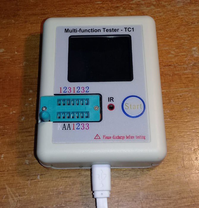
I didn't use my multimeter this time, but a handy little Chinese-made tool that guesses the type of tripole and its characteristics, which I wrote below.
I bought this device at a local store with the usual markup (welcome to France) but I needed it to test my old capacitors and it has other useful features so I didn't care that much. And it was sold by an old, reputable store :-)
The gain itself is not a big issue, as long as it's about > 20 and there is no point if it is >40 for this specific application. It's also good to see which parts are real lemons and should not be used in a circuit. For example, too high a leakage will disrupt my circuits. We have totally forgotten to take leakage into account in this century !
Measuring these parameters is not an exact science since germanium is very sensitive to heat (even from the fingers) and even to light (the black paint can't stop all the light if it's intense enough) so sometimes I had to make several measurements.
minifux1 :
hFE Vbe Ice0 106 210 5 34 224 31 204 7 156 219 1 193 21 164 ??? 36 232 29 229 36 248 32 132 30 115 14 44 167 14 40 195 7 32 239 36 131 1 120 195 7 46 215 86 200 7 26 213 38 210 33 268 31 219 48 124 4 49 195 14 21 210 30 200 7 22 224 31 219 14 173 161 35 26 205 5 ampliatubes:
hFE Vbe (mV) leak (µA) 40 126 4 59 205 7 42 220 37 200 14 23 221 8 34 214 14 42 219 24 232 1100 26 213 5 34 229 34 220 1 28 216 26 215 40 204 7 ?? 196 200 79 197 8 33 124 5 95 220 73 155 14 49 215 29 233 14 44 137 134 214 7 124 159 8 28 210 2 46 229 220 156 35 37 211 31 133 42 204 14 46 222 4 296?? 218 11 424 188 35 40 205 7 90 126 7 52 205 7 46 135 2 31 220 464 194 34 223 174 28 22 224 26 220 72 200 5
Verdict : one totally rotten lemon, several in bad shape, most are bitter but usable, but some have interesting characteristics and demand more examinations. Is their high gain real or an artefact ? and if they really have such a high gain, can they be used for more noble purposes than digital switching ?
I also wonder about those parts with Vbe < 200mV.
I didn't/couldn't check for the gain-bandwidth product (or rise and fall time). That should be for another time and for the high frequency dividers :-D
I guess about half of them would be used for the intended circuit (the shift registers, I need gains between 20 and 40 and no significant leakage). I might have to get more of them to complete the circuit because there are quite a lot of stages... but they have become so expensive !
Next step would be to plot the data in a graph and re-bin the stock, according to the various groups I identify in the dot cloud.
And yes, germanium is fun but silicon is so much better :-D I measure so little relative variations in new parts, even cheap ones...
Update 20230711
The next log tests more pieces and finds that the tester might be the culprit for the occasional (10%) lower Vbe.
. -
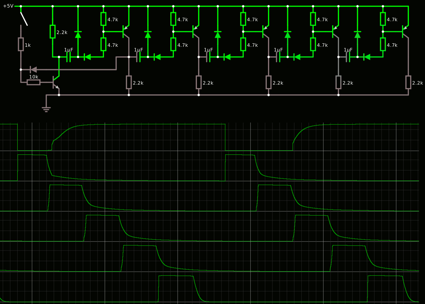
Reduction by mirroring
03/02/2020 at 02:28 • 0 commentsThe previous logs Pulser-sequencer and Towards a smaller shift register try to reduce the complexity (and parts count !) as much as possible but the last circuit was still pretty daunting and looks overkill. I couldn't figure out what was feeling wrong until... I tried to reverse the circuit, and that would save a whole layer !
So the new version both does the sequencing AND pulls the pass transistor bases. In the real/final version, the only transistor per bit will be a NPN, and it saves a bunch of auxiliary parts.
I added another transistor (+1D1R) at the start to format the input pulse length and the curves show
- very short pulse (it works nicely)
- long pulse (it works well too)
So far the cost is 1T 2D 1C 2R and the pass transistor would have the pulse-shortening circuit...
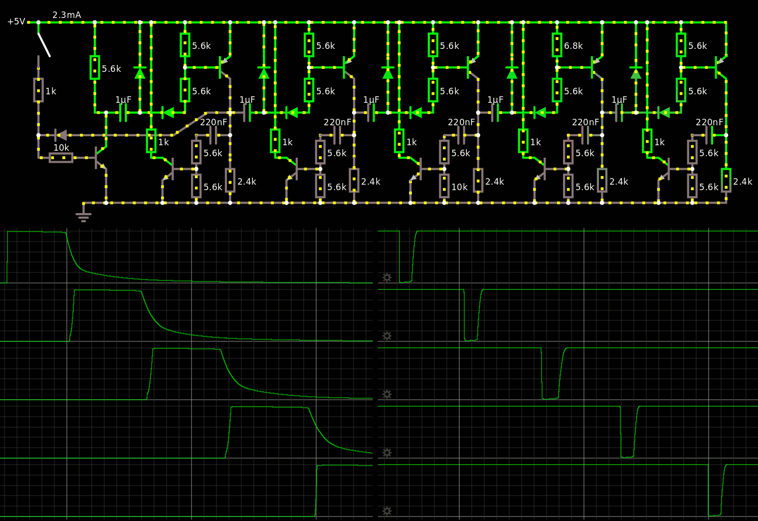
So the circuit is completed with the 2K2 pull-down replaced by the pass transistor and its RC cell. Here is the circuit :My inventory shows I have a quantity (tbd) of 5K6 and about 100× 2K4. The pulse width ratio is given by the ratio of the capacitor values. Here we have 1µF / 220nf so it's approx. 1/4 to 1/5. This provides a niiice clean edge ! If I find a large quantity of cheap non-polarized capacitors at about 1µF, I'll put 2 or 3 of them in parallel on the sequencer side, and only one on the pass transistor.
The power consumption is still very low when idle, and it can work for the slow parts : seconds, minutes, hours.
Note that for the sake of evaluation, the "pass transistor" here is a NPN with 1K to the positive rail but the final circuit will have the polarity reversed and the pass transistor (a PNP OC70) will not be tied to ground but to the other latches. I expect that the sequencer-side OC139 will work well.
The cost so far : 1P 1N 2D 2C 5R (11 parts, ignore the 1K pull-up)
-
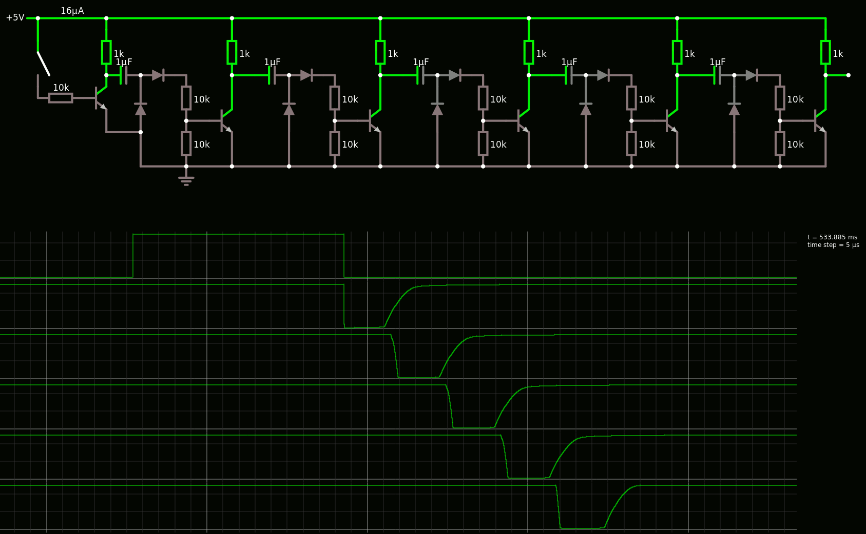
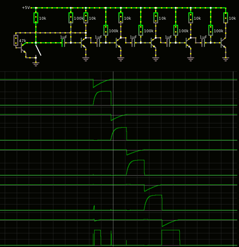
Pulser-sequencer
02/29/2020 at 21:48 • 0 commentsRemember the last logs : the goal is to use as few transistors as possible to send a string of consecutive non-overlapping pulses to several pass-gates. Here the design uses NPN as primary type but it will be reversed later because PNP are the majority type in Germanium and NPN are getting hard to get...
The last log Towards a smaller shift register has explored several methods but nothing satisfying yet.
Today I tried 2 new tricks :
- Feed the output back to the input
- use diodes to separate the stages and hopefully prevent the simulator to amplify spurious activity.
The first result is there :
The down and up edges are pretty clean though the output has a sort of slant after the first half of the pulse.
There is one great advantage here compared to the previous versions : the cell is triggered by a positive-going pulse, and the idle state does not draw any current. This saves power and reduces drift, compared to the almost-always-on earlier version.
The "cost" is 1P 1N 2C 3D 6R and can still be tuned.
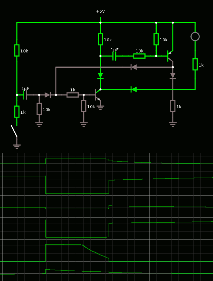
However when a resistor is replaced by a diode (to make a sort of charge pump) the result is even more interesting because 2 phases appear (source) :
The trailing edges are not as sharp but they are now significantly separated, there is a short pulse (going to the pass gate) and then the output to the next stage happens.
Apparently the sharpness of the trailing edges are not a critical parameter : (source)
I changed all values to 4K7 and it seems to help a bit.
I wonder if/how this circuit could be simplified...
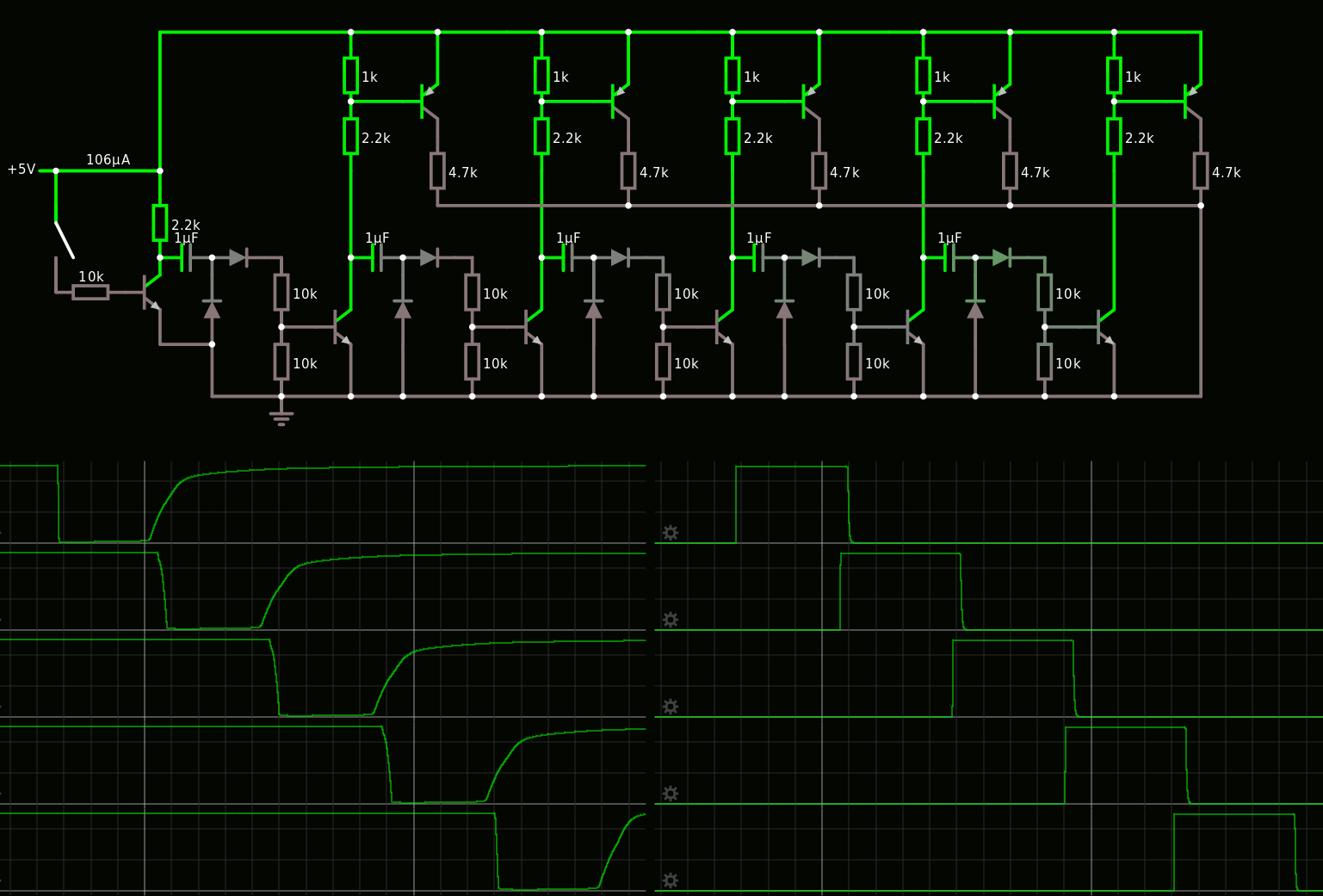
Trying to simplify the circuit and going back to the "first principles", I get this sequencer :
Falstad did some really strange things with the "charge-pump-like" diodes and capacitor, like creating one pulse of the low AND the high going input pulses, so I had to restart from a clean empty page and compare with real circuits (just to be sure).
The wave shape of this 5x sequencer doesn't look different from the previous one but it is way cleaner than the early attempts. Now I doubt that the feedback and more diodes are required.
Note that the capacitor "pull-up" resistor must be significantly smaller than the transistor's base resistors because otherwise, the "going-high" front will make a resistor divider equivalent through the capacitor, which reduces the effective voltage range on the divider network and reduce the pulse time.
The power is kept rather low, with about 5-8mA during activity, and mostly no current when idle. Only one cell is active at a time, except during transitions. The current is only dependent on the above-mentioned pull-up resistor that charges the capacitor before the up-going front when the transistor is released. That can easily be halved with a higher resistor (2K2) and/or a lower supply voltage.
Adding a simple complementary common-emitter cell creates overlapping pulses :
Adding a simple RC cell shortens the output pulse. The shape is not as sharp as I'd like but it's a minimal working circuit :
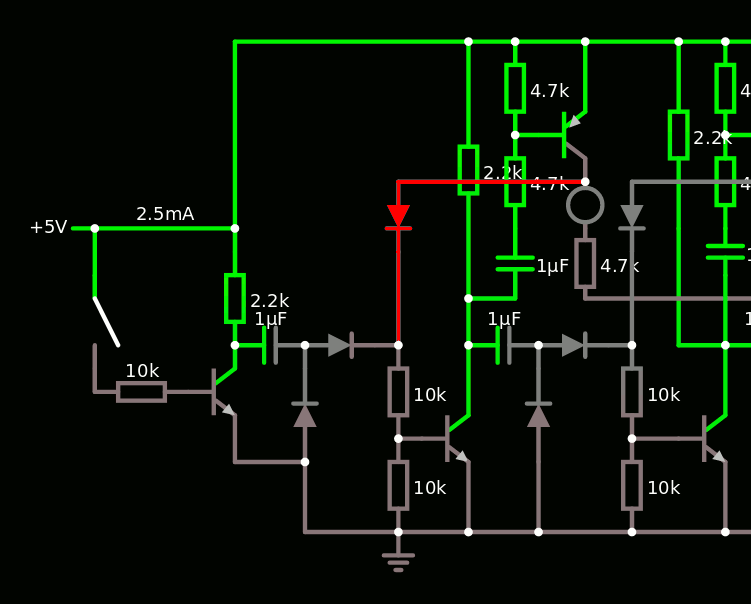
This saves quite a lot of diodes, compared to the circuit at the top of this page. And the feedback is not even used.
So it's working, the required power is reasonable, the pulses do not overlap and I can control the pulse widths with the corresponding RC constant...
I tried to remove the diodes but the sequencer would be much less reliable. This output drivers seem to work without diodes but the trailing edge is not clean.
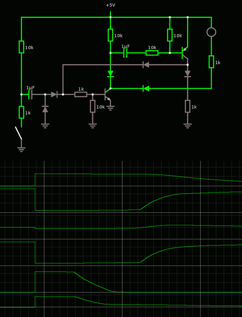
However, adding one diode as feedback brings some advantage :
It prevents the capacitor from discharging, until the PNP's output goes to 2 diode drops. The rising edge is delayed until a safer output level is reached. This prevents overlapping conduction for the rest of the circuit, AND both base resistors can now have the same value (they are 2×10K or 2×4K7 but now this difference is not required).
This new version also adds a series diode to the output buffer, to ensure that the voltage really drops low enough. However this might not be really necessary because the pass transistor has a Vbe drop as well. The output is cleaner anyway :
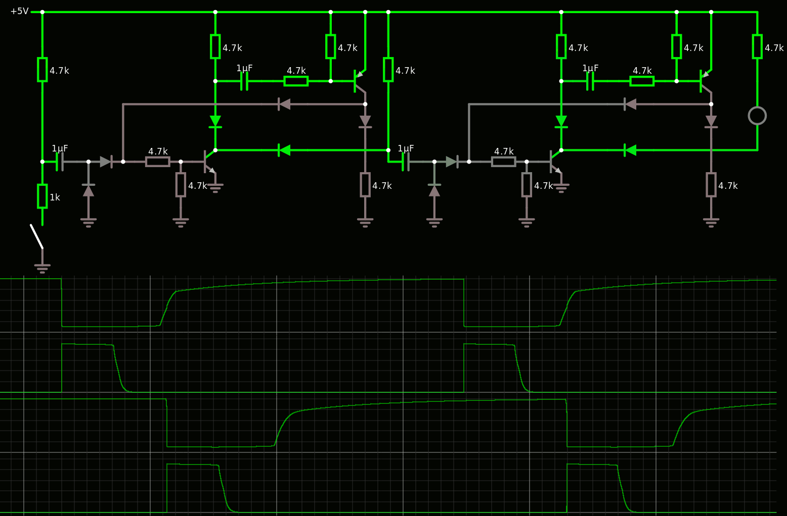
Now each bit slice has 2 transistors, 3(4?) diodes, 5 resistors...
-
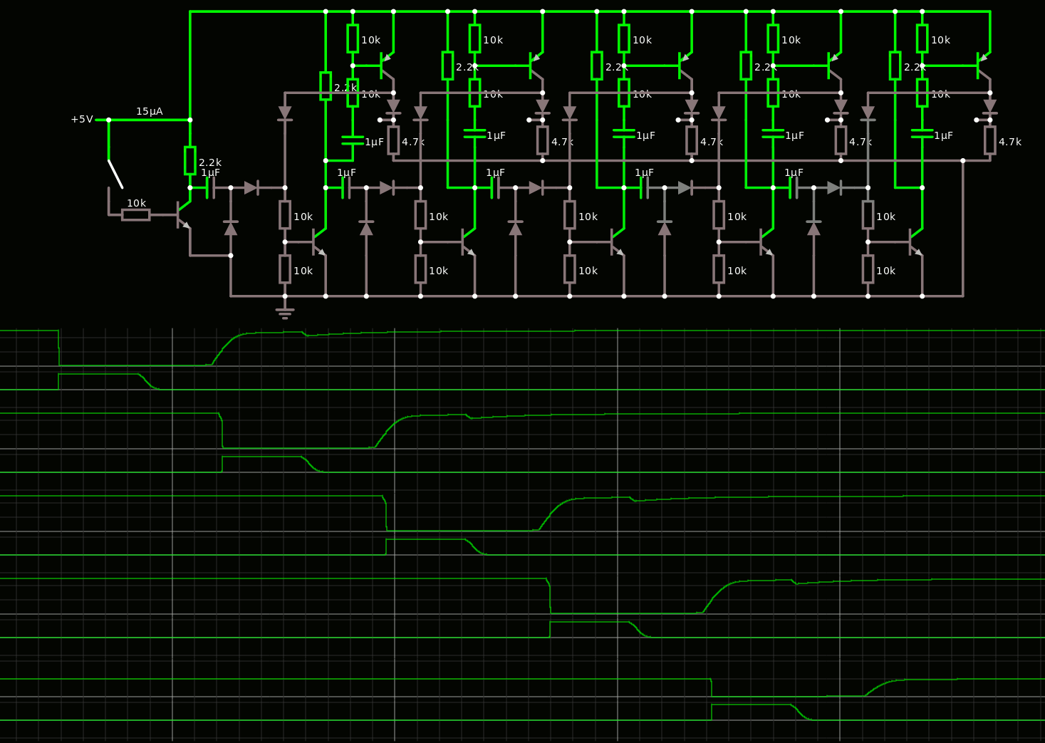
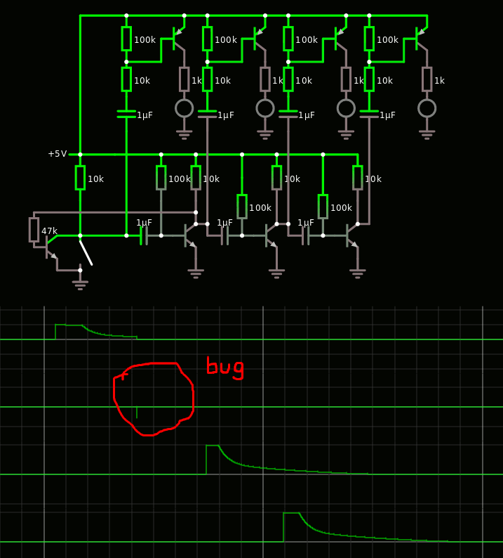
Towards a smaller shift register
02/28/2020 at 01:58 • 0 comments(see updates at the bottom)
_____________________________________________
I seem to have solved the problem of cascading the latest flipflops, using better decoupling (and some diodes ?). Here's the new circuit :
For the "fast" parts, a pull-down resistor would be required on the base of the pass transistors, to evacuate the base charges and "cut hard".
There is a better Power On Reset as well, and this system only uses 6 transistors because there is no need to invert the feedback data (just use an inverted value).
Then the challenge is to properly sequence the pulses to the pass transistors.
The question here is not to control a master and a slave latch, but a series of consecutive latches ! so there are as many pulses as there are latches. Here I focus on the "slow" part (< 1Hz update) with a string of one-shot pulsers :
I have really NO IDEA why the last stage emits multiple pulses... The mysteries of Falstad...
But the principle seems to be realistic : each bit of the shift register uses 2 T for the FF, 1T for the pass transistor and another for the pulse/delay. It's far from perfectly working but there is hope that each bit uses only 4 transistors. I might add some diodes to create a charge pump or something like that...
The "fast" circuits might need something more elaborate but at least I might have reduced the parts count for the H:M:S circuits ! (5+3+5+3+5+3)×4 (+ some control stuff) amounts to about a hundred transistors of the same polarity.
I'll try to make it work, then move to the faster parts : I have found a gorgeous vintage resonator at 2K5Hz !
That removes some pressure on the divider's design...
Update : That might work but the simulator is losing its sanity...
Sometime it wants to find crazy negative voltages at the collectors of the PNPs. I'll have to test it on the bench but it looks promising.
I must also find a way to "shape" the pulses because the "decay" is not very clean. But i'm getting closer to my goal :-)Cost : 1 PNP + 1 NPN (so it's the same when the polarity is reversed), overall : 5 transistors per bit of a shift register. For a whole display : that's about 120 + 6 transistors... This also facilitates the setting of the time because each shift register can receive a pulse, that could be from a button, and it's inherently debounced.
Stay tuned !
Thanks to Google Image search, I just found this :The page shows various enhancements to the system. I'll have to test it to improve my sequencer ! However if this trick works for 2 transistors, I wonder if/how it can work for more...
Clockwork germanium
A retro version of Yet Another (Discrete) Clock, with vintage parts