Open Source Multimeter
A relatively low-cost but full-featured and safe multimeter.
A relatively low-cost but full-featured and safe multimeter.
To make the experience fit your profile, pick a username and tell us what interests you.
We found and based on your interests.
Sorry about no updates for ages... But that's because nothing much has happened.
First off, I had difficulties soldering the micro onto the breakout board I'd made, eventually trashing the board (I've no idea about the chip), and I haven't made another board.
Then I had another project that I wanted a good (and true RMS) multimeter for, so I ended out buying one. That kind of removed much incentive for this project.
So I haven't got anything done, and probably won't either... I'll gladly help anyone who wants to take it from where I've left off, and I might have another go at doing the micro and proceed with the experiments on that end. We'll see...
Well, the MCUs and analog switches arrived a few days ago. I've made a very basic breakout PCB for the analog switches, and have started prototyping with them. I haven't done anything with the MCUs yet (and nor has the programmer arrived, so I couldn't do much more than make the breakout anyway).
On a slightly different note, I installed KiCAD on a different machine to check out opening the schematics (which I should have done long ago), and found a couple of issues. The worst, which is now fixed, is that the cache library didn't include the analog switch symbol. The other issue is that a few of the component footprints that I've made have pads with rounded rectangles – which requires a KiCAD version more recent than the latest Stable release. That would have happened because when I installed several months ago I chose the Unstable package (on Linux) as the alternative was the very old stable version – and since then, I've updated, and still have the unstable version. I'm not going to change the footprints to rectangle, because the PCB editor is a real pain about updating footprints, and also it would require a fair bit of layout work.
Also, I've changed my mind about building it: I will, but as a bench meter. I'll do it with several smaller / less complex PCBs (e.g. using the STM32F373 breakout I designed), no battery (or maybe a 9 V battery), no USB, and probably a higher voltage rail for the op-amps too.
Now for the initial results:
Read more »I've been busy on other things for the last while, so don't really have much progress to report.
First, a few days ago I was going to order some MCU chips, and found the place I was buying them from was sold out – with expected delivery in October or November! That kind of put me off...
But I decided that there were two things I needed to prototype / investigate, the MCU (particularly the ADC) and the input section. I don't have the analog switches or actual op-amps yet either, so I couldn't do a proper prototype. So I just did a quick test with a different op-amp (TLC274) as to how the input impedance affects the output. Result: a 1 megohm pot acting as a voltage divider applying approximately 2 – 10 mV to the op-amp (configured as a voltage follower) had a very similar output voltage whether connected directly to the positive input, or connected via 20 megohms – and connecting another 10 megohms to ground as a voltage divider produced the expected voltage as well. So looking good so far.
Today I discovered two things: one, I had a major mistake in my design; and two, the MCUs are back in stock! So I'm about to order them, the analog switches, the LCD, and a programmer for the MCU.
The mistake in my design was simple: U103, the reset chip, was powered by 3.3 V instead of directly from the battery! As it forces the MCU into reset when its supply is below 3.5 V, it would never have come out of reset. Fortunately, it was easily fixed as +BATT was already available nearby on the PCB.
Unfortunately, this probably never going to get past a prototype. To get the PCB made for me would cost nearly as much as the rest, and put the total cost far higher than I'm willing to pay. I could possibly make it myself, but I'm not particularly confident in my abilities to make one that large, at least not unless I can improve the quality of the masks for exposing the photoresist – which would probably require a better printer to prevent the light bleeding through.
For prototyping I'm going to need a breakout board for the micro, so I had a look at what I could find. All the breakouts I could see for QFP64 pinouts had holes on all four sides, which is unsuitable for breadboards. I guess jumper leads would work, but still... So I designed my own. In fact, I went a step further and made it a bare-minimum dev board for the STM32F373 as well – it has the decoupling caps for power and the reference voltages, a power setup so that it can be powered off a single rail, and a programming header. But don't install any components, cut the net ties in the ground, and it is simply a QFP64 to DIP breakout. It has a standard DIP pinout, and fits a breadboard nicely – well, if spanning two slots (i.e. 1" wide) and taking 32 rows is "nicely"!
I've written a bit of documentation trying to explain what everything does... I probably miss a lot of important stuff and mention a lot of obvious stuff too, but at least it did lead to me discovering several issues.
The biggest change was to base +V_int (now badly named!) off +3.3VA (analog rail) instead of the battery. This let me use a lower clamping voltage, which in turn let me use it to power the analog switches – which fixed an issue of them having a significant overvoltage applied when significant clamping occurred. It also means I only have two ground rails now.
The other notable change was to the anti-aliasing filter. Previously I'd messed up the formula, and had the capacitors several times too large. I have also changed it to be a differential filter so that the ADC doesn't affect either the signal or common line unduly.
Since my last update I've sorted out the clearances I had mentioned (and a couple more that I found), and I've added copper pours / zones. I have also sorted out connecting the different grounds.
I originally intended to connect across the jumpers in the schematic after laying out the PCB. After doing that, the zones were associated with the old nets which no longer had any connections, and changing the nets to the new ground connected it to all the ground pins in the zone irrespective of which ones they should be connected to. So obviously that wasn't going to work.
After a bit of searching the internet, I found out that what I was looking for is (at least sometimes) called a "net tie". To do this in KiCad, the best way is to create a special footprint with the two pads, and a graphic line on a copper layer connecting the two – DRC ignores graphic lines, even when on copper layers. I created a footprint like that, set the jumpers' footprints to it, and it worked great.
So my next steps are going to be a bit of prototyping!
As per the title, I've managed to get the initial PCB layout done. It isn't pretty, and I don't like the idea of making it by hand as I had intended, but it should work – barring faults in my schematic (of which there are probably at least a few), routing (possible, but I hope not!) or footprints (hopefully none). Ideally I'll add some copper pours, but I've got to be careful with that because of potentially high voltages in some areas – and on that note, I've got to adjust a few traces to ensure correct clearances around the two current-measurement terminals.
So here's some pertinent details about the design of the PCB:
As was almost suggested by a comment recently, I have added a PDF version of the schematics to GitHub.
And due to the same comment (thanks!), I have added a capacitor to the battery voltage sensing, which should solve any issue with the voltage divider impedance vs. the ADC source impedance.
In working on the PCB layout, I also decided that my universal SMD capacitor / resistor footprints (accepting anything from 0603 to 1210) were too big to be workable when it came to decoupling capacitors for the MCU. I also decided that it is unlikely for anyone to want to use sizes quite that big, so dropped the sizes a bit – now capacitors 1 uF and under are 0603 to 0805, and 10 uF capacitors are 0603 to 1206. Still got a lot of fun routing around the MCU to go though.
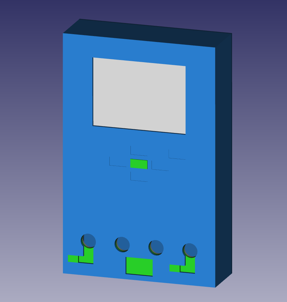 And the other noteworthy news is that I've updated the External Design CAD model – you can see a render on the right, although the colours won't end up like they are there.
I intend to make the case from FR4, as was suggested by a comment on my first external design project log (thanks!) and I learnt about from this Hackaday article. It won't all be soldered, epoxy will see significant use as well.
The green down the bottom is the USB port cover – slide it right to cover the terminals, and then up to uncover the USB port. This is necessary because I want USB for charging, and I'm not putting an isolated switching power supply in there.
I've updated the schematics – the commit log on GitHub should give a fairly good summary of the changes. The most important changes are adding a speaker (for continuity checks), a reset IC (to shut it down if the battery voltage is too low), changed the battery charger IC to one that can check the battery's thermistor, and made it so I can monitor the battery voltage.
With regards to monitoring the battery voltage, I've done that simply with a voltage divider feeding the ADC. My voltage divider divides by two with 1 M resistors, so that gives a current of ~2 uA depending on battery voltage. The maximum source resistance of the ADC is stated as 50 k, so I'm definitely not going to get an accurate reading of the actual voltage. I'm not concerned, because I'm only interested in knowing the battery state of charge – and I'm sure I'll be able to determine that just fine.
The PCB layout is progressing nicely.
The case design will be changing slightly from the graphic I've got right now, and I should update that soon too.
As promised in my previous log, I've got the initial schematics up on GitHub. Most components don't have values or part numbers yet, and some of the op-amps are placeholders for the actual parts used – but they still show the design just fine, and I think that's what matters right now.
Create an account to leave a comment. Already have an account? Log In.
Perfect, thanks! I never even thought about doing that... I'll have to use the excuse that I decided to add that part way through posting the update instead of saying it was missing, and didn't think too hard!
Re PDF schematics, you're right that I don't have any – mostly because I never thought about doing it yet. I'll put a PDF version up tomorrow.
I see you are aiming for safety but it looks like the USB is a direct connection. I was wanting to set up a bench DMM that was not battery powered and could connect to the bench PC. With minor mods it looks like this project could meet my needs so I'm watching with interest.
Yes, it is a direct connection. However, I am designing the case so that it cannot be plugged in at the same time as the measurement terminals via a mechanical interlock – a panel that slides to cover the terminals then to uncover the USB port, or vice versa. So it should be safe.
Obviously that isn't the solution for what you want. I looked into doing it how you would want, but decided it wasn't worth it for me. It is definitely possible though – you'd need some kind of isolation for the data lines (and for USB that isn't easy (bi-directional differential pair) or is fairly expensive (e.g. http://www.analog.com/en/products/interface-isolation/isolation/standard-digital-isolators/adum4160.html), or you can use a separate USB-to-Serial / SPI / whatever chip and isolate those data lines (which is much easier)), and you'd also need an isolated switching power supply to isolate the power lines – or you could have a separate (isolated) power supply and only use USB for data.
I think the task to build a multimeter with any feature you want is already available.
Check the link below for a processor controlled multimeter you can customize to your needs without wasting all your time calibrating and guessing if its going to be accurate.
They have many other options too.
Of course the problem is already solved. By big companies with closed-source products where everything is as well hidden as possible in fancy integrated circuits such as that one. I want to solve it for myself, and to share the results with everyone.
Any item built with it, even if open-source, is going to depend on it which is very much contrary to my goals.
That doesn't really help one bit with calibration or accuracy. The input resistors are not built in, and therefore all that is dependent on the components used. It's really just a fancy ADC and DAC with built-in support for some of the features needed for a multimeter (such as the input circuitry switching). But only some – it doesn't support AC without an external support circuit (which includes a dedicated IC if you want true RMS). The interesting part of this project isn't making a product, it is designing everything.
I won't be guessing whether mine is accurate, I will calculate the exact accuracy limits based on the components and techniques used.
Even if I did want to go that route (I don't), what would they cost? I'm guessing more (in total, not each) than what I'll spend to do it all myself. In fact, more than buying a multimeter with the features it supports (because in reality, its feature set is very definitely limited).
I guess you have conflicting goals. Do you understand The difficulty multiplexing all those analog input levels into multiple functions? Sounds like you just want to do it yourself! You can buy multimeters with that chip in them for $6.00, therefore you will not be doing it cheaper, more accurate or anywhere close to its features for less than that. That chip could be the basis for a multimeter where you can create whatever multimeter features you neglected to document are lacking in available units for cheap.
In general, you pay a lot more for developing something that is already off the shelve. The only thing you get in return is that you have learnt something and not saving money.
You are not going to be able to have the first proto working 100%, so how many times you have to rebuild it or replace/mod parts? Your cost goes up right there. Ignore for the fact that you'll need equipments and working multimeter to test it.
A big company spread the NRE over a large volume of units. They have volume discount on their parts. If they need to make a matching resistor network with laser trim, they can.
Certifying the multimeter or making one that will pass the test aren't exactly cheap. It can't be called safe unless it is certified and it is meant for something that goes through a production run and not a single quantity build copy/paste off the internet. How are you even going to do a test that might be destructive?
To do thing safely, you have to understand the safety design rules and the testing procedures. Go read up on Mooshimeter blog to see how they develop their meter and see how they solve their problems along the way.
Yes, I do want to do it myself. That's a large part of this. Why would I go to all the work of making it myself and only saving a little, or even spending more, to just use an off-the-shelf part that does most if not all of the harder parts for me? I like a good challenge, and without it I can't be bothered doing a lot of work to get something I could buy relatively cheaply.
This isn't an idea I've just thought of (I've been thinking about it on and off for almost a year, and spending a fair bit of time of it), so yes, I have thought about things like multiplexing the inputs. There's almost definitely some more issues that will arise though.
My point about price is that after having a quick look, the prices I saw were at least US$60 for ten. As I'm only building one unit, I'd basically be throwing away nine chips and putting the cost of ten of them into one meter. I'd sooner buy a US$35 Uni-T UT139B (with free shipping), which was what I was considering – and what I'll still do if I don't like the price of this after working out the design.
You're absolutely right, on all points.
If I can learn from it without spending too much in excess of just buying a meter, then as far as I'm concerned it is time and money well spent. And I've already learnt some things from the work I've done thus far without spending anything. But if I discover after spending only time that it is going to require a significant monetary expenditure, I will just buy an off-the-shelf meter.
I'm obviously not going to get a one-off certified, but if (and it is a very big if) I found a demand for it as a product, I would definitely either get it certified or not sell it at all. For now, I intend to, as far as possible, over-design it so that I'm happy with it – and preferably, so that everyone on here is too. And then I'll probably only use it in ways that mean most of that is totally unnecessary (i.e. on less than 50 V DC)!
Right now, for potentially destructive tests I intend to do them with only the relevant parts in place, possibly with cheap substitutions where relevant – e.g. no ADC, cheap op-amps for the buffers. That way if anything is damaged, it is only relatively cheap parts. Then once everything seems good, test it with the actual components. Unfortunately, transient testing probably won't be one of the tests...
After seeing your comments to me and your responses to others, I wonder why you have created this project at all.
"I intend to design and hopefully build a fully open-source multimeter. It will be designed with safety in mind (intended to meet CAT III 600 V), with very good accuracy and lots of features. I want to keep the price low. I am mainly designing it because I am personally looking for a good but cheap meter and am not satisfied with the available offerings."
You don't even know what your goals are (features). Projects with no goals or poorly defined ones seldom go anywhere. They linger forever. They surely are not good open source projects. Is this your first project?
You seem to be insulted by big companies with closed-source products with cost effective solutions. The closed-source company (Cyrustek) I pointed you to would let you build a multimeter with a huge set of features of your choosing for cheap. Which by the way is what you said was your main reason for "trying" to do this project. A wooden case ? LOL
P.S. I will be checking in, in a few months to see if you have figured out your goals yet.
There is not much reason to make a "Safe" DMM and an "Accurate" DMM at the same time. Accurate DMM is achievable for prototype quantities if you are careful with your design. I won't question that except to say there are cheaper and more accurate alternative on the used market. The old equipments are well documented and often service manual are available if you look. Even reading them give you some insights on how they work.
Safety on the other hand isn't. This sums it up pretty well. For high voltage stuff, you often don't need 6 significant +/- 0.01% accurate results.
http://ecmweb.com/content/does-your-meter-safety-measure
>Price need not be an obstacle to safety. When making simple voltage measurements, a low-cost alternative to a full function meter is a voltage tester. Testers designed in the last two years are now available in both CAT III-600V and CAT III-1000V ratings at prices well under $100. No electrical worker should compromise personal safety for financial, or other, reasons.
>To get certified, the meter must pass the mandated tests. Look for independent certification, not just for words saying "designed to meet" or "conforms to IEC 61010." Those statements are no substitute for independent testing. Many engineering designs have not survived real-world testing.
You know Fluke make their own CATIII fuses and their fuses is actually cheaper for retails than other fuses on the market. They are $6 a piece. Do you have access to the CATIII specs and test procedure? Most of these standards or the equipment to test them aren't cheap.
Not sure about flammability of wooden cases nor how repeatable for that for something that is to be certified.
Read up on Mooshimeter. It is CATIII with open source software. They have to go back making new case designs a few times.
Not sure if I can take this seriously "it doesn't support AC without an external support circuit (which includes a dedicated IC if you want true RMS" You know that Analog Devices have some very bright engineers that make these RMS converters. These guys have a lot of experience and spend designing an analog chip that everyone else uses them externally for you guess it RMS meters. Do you think you can do better?
First off, wood is only for my prototype. I wouldn't even consider it for anything else.
I've posted quite a few features / goals in a log.
That chip would let me build something cheap, if I was building enough of them. I didn't see anywhere selling less than 10. If I've missed somewhere worth considering, then that might change things slightly – it does seem very good for what it does.
Used is good, but because of where I live I don't have access to a lot of it unfortunately, or at least not without significant shipping costs.
Version 2 of the standard (version 3 is current) is available for free online, I think from one of the associated standards bodies (for a country or region-specific version). But you're right, wood wouldn't meet it, nor could I test most of it, and safety is very important. Maybe I should just remove that entire goal and stick with something only rated to +/- 100 V peak (hence only working with extra low voltage rather than "low voltage")?
All multimeters have a limited bandwidth, so if I sample the signal fast enough I should be able to easily calculate the RMS value in software.
The problem is that most of the high res ADC which is what I assume you'll be using have really really low sampling rates probably in the low kHz. So if the waveform is complex (i.e. non-sinusoidal), you'll need to sample higher harmonics as well which doesn't give you much bandwidth. And these are the type you'll want to measure in RMS - otherwise a half wave with scaling get you the results.
Take a look at the bandwidth of their RMS converter...
http://www.analog.com/en/products/linear-products/rms-to-dc-converters.html
Lowest ones is 450kHz. Can you do that in software?
No, I can't do anything like a 450 kHz bandwidth. However, the meters I was looking at are more like 1 kHz, maybe as much as 10 kHz, and I should be able to do that – the ADC I'm thinking of has a sampling rate of up to 250 kHz.
I was referring more to the categories of wiring / source rather than measurement (https://en.wikipedia.org/wiki/Extra-low_voltage), so I shouldn't have even mentioned it (especially as I got the values wrong). But looking at that page you posted (and some others too), it seems I'm really only interested in CAT II – I had previously read a Fluke page that seemed to be suggesting that a normal outlet right near the fuse box would be classed as CAT III...
You are not going to full ADC accuracy at full speed.
e.g. AD7176-2
17 noise free bits at 250 kSPS
20 noise free bits at 2.5 kSPS
22 noise free bits at 5 SPS
They don't even guarantee the minimum guaranteed values and only listed under typical.
Agreed. However, the value displayed is basically an average (whether arithmetic mean or RMS, the former for the DC offset and the latter for AC) over somewhere in the vicinity of 60,000 samples, so I would expect that should remove the effect of most noise. I know averaging won't help with distortion, INL, or anything like that.
Nice work. I had a similar idea but did not pursue it. I was thinking of using the properties of matched components (monolithic resistors/transistors) as a reference rather than absolutely tuned reference voltages/currents. I'm not sure if it would work but just a thought. I'm trying to see the matching characteristics of PCB traces in a fab process (e.g OSHpark) to see if they can be used.
Thanks!
Using matched resistors is a great way to get a voltage divider or similar with an extremely accurate ratio, but that's about all I can see it giving other than comparative measurements (e.g. this voltage is double that one) which don't actually need that accuracy most of the time. You still need an absolute value somewhere to get a measurement in actual units. The ADC output is just the ratio of the input to its reference, and combining that with more ratios still leaves a ratio – and the only way to turn a ratio into an absolute value is to combine it with one (the reference), and the accuracy of the resulting value can only be as good as the reference.
So maybe I'm missing something, but I don't think an accurate voltage reference can be avoided, nor an accurate current reference (possibly via an accurate resistance) for current or resistance measurement. I'd be interested to hear if I am wrong though!
Nicely explained. You are right that an absolute reference is required somewhere in there to convert relative parameters to absolute.
On my old multimeter resistance measurement, they use the precision divider network in series to the constant current source and use that voltage drop as reference to the ADC, so resistance measurements are measured against the network NOT precision voltage reference. They can use a +/- 10% constant current and still get the same results.
If they had the reference voltage to generate constant current, they would have to worry about DC offset and other additional errors on the sampling resistors.
@K.C. Lee That's clever. I was intuitively thinking of such a circuit where the final measurement number would have the reference cancelled from the equation. Something like a bandgap reference
Yes, that will work great and is similar to what I intend to do. But they still have an accurate absolute reference in the form of the value of at least one resistor in the network. Matched components generally have a very accurate ratio but relatively loose tolerances on absolute values.
Become a member to follow this project and never miss any updates
 Jonathan Bruneau
 Paul Andrews
 John Duffy
 jaromir.sukuba
Regarding the battery voltage measurement (1M voltage divider): I can not see your schematic as I don't use KiCAD and can not find a PDF version. So I don't know, if you have a capacitor at the ADC input (after the voltage divider). If you have it then the 50k Input impedance limit of the ADC does not matter. Something between 100nF and 1µF is normally good. If not, I suggest to add it.