 Karl S
-
Update...
06/07/2017 at 05:54 • 0 commentsSorry about no updates for ages... But that's because nothing much has happened.
First off, I had difficulties soldering the micro onto the breakout board I'd made, eventually trashing the board (I've no idea about the chip), and I haven't made another board.
Then I had another project that I wanted a good (and true RMS) multimeter for, so I ended out buying one. That kind of removed much incentive for this project.
So I haven't got anything done, and probably won't either... I'll gladly help anyone who wants to take it from where I've left off, and I might have another go at doing the micro and proceed with the experiments on that end. We'll see...
-
Initial prototype results
09/02/2016 at 06:23 • 0 commentsWell, the MCUs and analog switches arrived a few days ago. I've made a very basic breakout PCB for the analog switches, and have started prototyping with them. I haven't done anything with the MCUs yet (and nor has the programmer arrived, so I couldn't do much more than make the breakout anyway).
On a slightly different note, I installed KiCAD on a different machine to check out opening the schematics (which I should have done long ago), and found a couple of issues. The worst, which is now fixed, is that the cache library didn't include the analog switch symbol. The other issue is that a few of the component footprints that I've made have pads with rounded rectangles – which requires a KiCAD version more recent than the latest Stable release. That would have happened because when I installed several months ago I chose the Unstable package (on Linux) as the alternative was the very old stable version – and since then, I've updated, and still have the unstable version. I'm not going to change the footprints to rectangle, because the PCB editor is a real pain about updating footprints, and also it would require a fair bit of layout work.
Also, I've changed my mind about building it: I will, but as a bench meter. I'll do it with several smaller / less complex PCBs (e.g. using the STM32F373 breakout I designed), no battery (or maybe a 9 V battery), no USB, and probably a higher voltage rail for the op-amps too.
Now for the initial results:
- I rediscovered that parasitic capacitance combined with a 10 megohm input impedance creates a very effective low-pass filter – with a significantly lower bandwidth than I'd like. I did realise this earlier, and decided then that I'll just play tricks in software to compensate (although that reduces effective resolution in that range).
- The switch off leakage is very low (max 5 nA @ 25 C, max 50 nA @ 85 C), in fact lower than anything else I've seen, but is still very significant when dealing with a few megohms. I've thought of a few ways of combating this.
For dealing with leakage, there's two scenarios to consider: the input voltage divider for higher voltages, and the gain selection for the lower voltages and the output current sense. In both cases, the issue is leakage current flowing through the switch, altering the ratio. I can't just calibrate it out, because the actual current will be extremely temperature-dependent.
On the input voltage divider, I could potentially connect the (buffered) division result to the COM-side resistor, between it and the switch (which connects it to COM). But that's positive feedback into the op-amp, and the input offset voltage might upset things too. However I'm not sure what else is possible, so probably the route I'll take. There's a couple of ways I could actually do it: have a second set of switches to connect it in (and a NOT gate each, because I don't have enough GPIOs), or connect it to the same location via a moderate-value resistor. I've tested them both slightly, and both seem to work. I don't like the former because of the component and layout implications, but I don't like the latter because it would force me to use the buffered version of COM (to deal with the current through the resistor when that range is on) which makes problems from the input offset voltage of that op-amp. However, I think I can handle the maths for the latter (and besides I probably have the same thing on the low-voltage ranges), so it is the option I'll go for – unless you can give me some better ideas!
For the low-voltage input and output current sense amplification, I could do the same thing, although I would have to add op-amps to buffer the value to feed back. The other way would be to have an amplifier for each ratio, and select which one to use – probably better, but more hardware.
I haven't updated the circuit for any of these changes yet, because I still haven't decided what to do – and I don't want to do it over again. And I just noticed I messed up the output current sense amplifier gain resistors, but I'm not fixing it until I'm sorting out the rest.
-
An update...
08/14/2016 at 23:11 • 0 commentsI've been busy on other things for the last while, so don't really have much progress to report.
First, a few days ago I was going to order some MCU chips, and found the place I was buying them from was sold out – with expected delivery in October or November! That kind of put me off...
But I decided that there were two things I needed to prototype / investigate, the MCU (particularly the ADC) and the input section. I don't have the analog switches or actual op-amps yet either, so I couldn't do a proper prototype. So I just did a quick test with a different op-amp (TLC274) as to how the input impedance affects the output. Result: a 1 megohm pot acting as a voltage divider applying approximately 2 – 10 mV to the op-amp (configured as a voltage follower) had a very similar output voltage whether connected directly to the positive input, or connected via 20 megohms – and connecting another 10 megohms to ground as a voltage divider produced the expected voltage as well. So looking good so far.
Today I discovered two things: one, I had a major mistake in my design; and two, the MCUs are back in stock! So I'm about to order them, the analog switches, the LCD, and a programmer for the MCU.
The mistake in my design was simple: U103, the reset chip, was powered by 3.3 V instead of directly from the battery! As it forces the MCU into reset when its supply is below 3.5 V, it would never have come out of reset. Fortunately, it was easily fixed as +BATT was already available nearby on the PCB.
Unfortunately, this probably never going to get past a prototype. To get the PCB made for me would cost nearly as much as the rest, and put the total cost far higher than I'm willing to pay. I could possibly make it myself, but I'm not particularly confident in my abilities to make one that large, at least not unless I can improve the quality of the masks for exposing the photoresist – which would probably require a better printer to prevent the light bleeding through.
-
Added STM32 breakout board
07/18/2016 at 09:35 • 0 commentsFor prototyping I'm going to need a breakout board for the micro, so I had a look at what I could find. All the breakouts I could see for QFP64 pinouts had holes on all four sides, which is unsuitable for breadboards. I guess jumper leads would work, but still... So I designed my own. In fact, I went a step further and made it a bare-minimum dev board for the STM32F373 as well – it has the decoupling caps for power and the reference voltages, a power setup so that it can be powered off a single rail, and a programming header. But don't install any components, cut the net ties in the ground, and it is simply a QFP64 to DIP breakout. It has a standard DIP pinout, and fits a breadboard nicely – well, if spanning two slots (i.e. 1" wide) and taking 32 rows is "nicely"!
-
Some documentation added
07/14/2016 at 04:01 • 0 commentsI've written a bit of documentation trying to explain what everything does... I probably miss a lot of important stuff and mention a lot of obvious stuff too, but at least it did lead to me discovering several issues.
The biggest change was to base +V_int (now badly named!) off +3.3VA (analog rail) instead of the battery. This let me use a lower clamping voltage, which in turn let me use it to power the analog switches – which fixed an issue of them having a significant overvoltage applied when significant clamping occurred. It also means I only have two ground rails now.
The other notable change was to the anti-aliasing filter. Previously I'd messed up the formula, and had the capacitors several times too large. I have also changed it to be a differential filter so that the ADC doesn't affect either the signal or common line unduly.
-
PCBs completed
07/04/2016 at 09:31 • 0 commentsSince my last update I've sorted out the clearances I had mentioned (and a couple more that I found), and I've added copper pours / zones. I have also sorted out connecting the different grounds.
I originally intended to connect across the jumpers in the schematic after laying out the PCB. After doing that, the zones were associated with the old nets which no longer had any connections, and changing the nets to the new ground connected it to all the ground pins in the zone irrespective of which ones they should be connected to. So obviously that wasn't going to work.
After a bit of searching the internet, I found out that what I was looking for is (at least sometimes) called a "net tie". To do this in KiCad, the best way is to create a special footprint with the two pads, and a graphic line on a copper layer connecting the two – DRC ignores graphic lines, even when on copper layers. I created a footprint like that, set the jumpers' footprints to it, and it worked great.
So my next steps are going to be a bit of prototyping!
-
Initial PCB layout done
07/02/2016 at 04:25 • 0 commentsAs per the title, I've managed to get the initial PCB layout done. It isn't pretty, and I don't like the idea of making it by hand as I had intended, but it should work – barring faults in my schematic (of which there are probably at least a few), routing (possible, but I hope not!) or footprints (hopefully none). Ideally I'll add some copper pours, but I've got to be careful with that because of potentially high voltages in some areas – and on that note, I've got to adjust a few traces to ensure correct clearances around the two current-measurement terminals.
So here's some pertinent details about the design of the PCB:
- 2 layers
- 130 mm x 90 mm board
- Minimum track width and clearance are both 0.25 mm (0.984 mil) – the maximum possible for components with a 0.5 mm pitch.
- Via size is 1.8 mm with a drill size of 0.8 mm.
- It should be possible to make by hand at home – the biggest annoyance would be the 246 holes, of which 98 are through-hole components or headers, 141 are vias, and 7 are mounting holes.
-
PDF schematics and updated external design
06/22/2016 at 08:32 • 0 commentsAs was almost suggested by a comment recently, I have added a PDF version of the schematics to GitHub.
And due to the same comment (thanks!), I have added a capacitor to the battery voltage sensing, which should solve any issue with the voltage divider impedance vs. the ADC source impedance.
In working on the PCB layout, I also decided that my universal SMD capacitor / resistor footprints (accepting anything from 0603 to 1210) were too big to be workable when it came to decoupling capacitors for the MCU. I also decided that it is unlikely for anyone to want to use sizes quite that big, so dropped the sizes a bit – now capacitors 1 uF and under are 0603 to 0805, and 10 uF capacitors are 0603 to 1206. Still got a lot of fun routing around the MCU to go though.
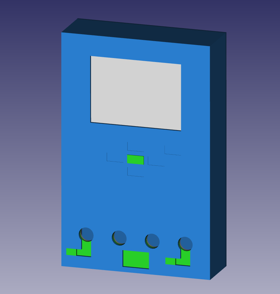
![]() And the other noteworthy news is that I've updated the External Design CAD model – you can see a render on the right, although the colours won't end up like they are there.
And the other noteworthy news is that I've updated the External Design CAD model – you can see a render on the right, although the colours won't end up like they are there.I intend to make the case from FR4, as was suggested by a comment on my first external design project log (thanks!) and I learnt about from this Hackaday article. It won't all be soldered, epoxy will see significant use as well.
The green down the bottom is the USB port cover – slide it right to cover the terminals, and then up to uncover the USB port. This is necessary because I want USB for charging, and I'm not putting an isolated switching power supply in there.
-
Schematics updated
06/21/2016 at 06:12 • 0 commentsI've updated the schematics – the commit log on GitHub should give a fairly good summary of the changes. The most important changes are adding a speaker (for continuity checks), a reset IC (to shut it down if the battery voltage is too low), changed the battery charger IC to one that can check the battery's thermistor, and made it so I can monitor the battery voltage.
With regards to monitoring the battery voltage, I've done that simply with a voltage divider feeding the ADC. My voltage divider divides by two with 1 M resistors, so that gives a current of ~2 uA depending on battery voltage. The maximum source resistance of the ADC is stated as 50 k, so I'm definitely not going to get an accurate reading of the actual voltage. I'm not concerned, because I'm only interested in knowing the battery state of charge – and I'm sure I'll be able to determine that just fine.
The PCB layout is progressing nicely.
The case design will be changing slightly from the graphic I've got right now, and I should update that soon too.
-
Initial schematics up!
06/09/2016 at 00:40 • 0 commentsAs promised in my previous log, I've got the initial schematics up on GitHub. Most components don't have values or part numbers yet, and some of the op-amps are placeholders for the actual parts used – but they still show the design just fine, and I think that's what matters right now.
Open Source Multimeter
A relatively low-cost but full-featured and safe multimeter.
 And the other noteworthy news is that I've updated the External Design CAD model – you can see a render on the right, although the colours won't end up like they are there.