Kuldeep Singh Dhaka
-
FFT and Box0
02/10/2017 at 21:26 • 0 commentsWhat is FFT?
Wikipedia says (Fast Fourier transform):
A fast Fourier transform (FFT) algorithm computes the discrete Fourier transform (DFT) of a sequence, or its inverse.Im not going to bombard you with mathematical details (its for another day ;).
What we are today going to do is, capture some real electrical signal with Box0 and visualize it.There are alot number of education video on Fourier transform on the Internet (example: Youtube).
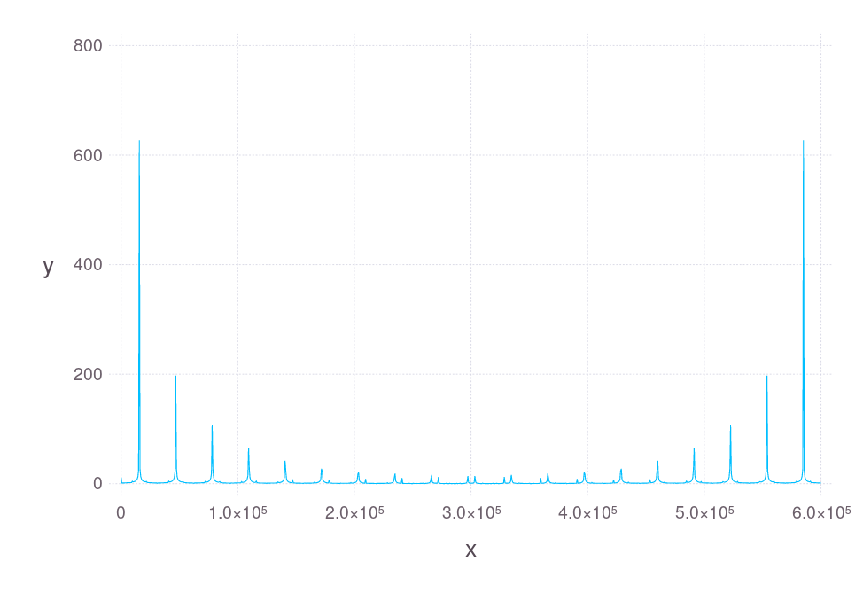
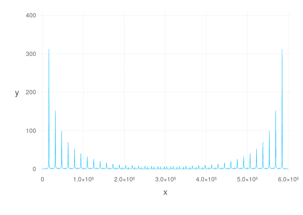
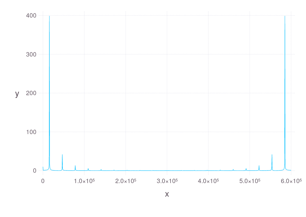
So, here are some plot that i captured with the code i wrote (code at the end of page).
Sine wave (15.6 KHz)
![]()
Square wave (15.6 Khz)
![]()
Saw tooth wave (15.6 Khz)
![]()
Triangular wave (15.6 KHz)
![]()
Python Code
import box0
import numpy as np
import matplotlib.pyplot as plt
import scipy.fftpack

##### PART 1 - Capture

# Allocate resources
dev = box0.usb.open_supported()
ain0 = dev.ain()

# Prepare AIN0 for snapshot mode
ain0.snapshot_prepare()

# Read data from AIN0
bitsize, sampling_freq = ain0.bitsize_speed_get()
data = np.empty(1000, dtype=np.float32)
ain0.snapshot_start(data)

# Free the resources
ain0.close()
dev.close()

##### PART 2 - Process

# perform FFT on captured data
fft_amp = np.abs(scipy.fftpack.fft(data))
fft_freq =  np.linspace(0, sampling_freq, len(fft_amp))

##### PART 3 - Visualize
fig, ax = plt.subplots()

# Show the time domain results (unable to show both plot at once - fix later!...never ;)
#time_x = np.linspace(0, len(data) / sampling_freq, len(data))
#ax.plot(time_x, data)

# Show the frequency domain results
ax.plot(fft_freq, fft_amp)

plt.show()
Julia Code
import Box0 import Gadfly ##### PART 1 - Capture # Allocate resources dev = Box0.Usb.open_supported() ain0 = Box0.ain(dev) # Prepare AIN0 for snapshot mode Box0.snapshot_prepare(ain0) # Read data from AIN0 bitsize, sampling_freq = Box0.bitsize_speed_get(ain0) data = Array(Float32, 1000) Box0.snapshot_start(ain0, data) # Free the resources Box0.close(ain0) Box0.close(dev) ##### PART 2 - Process # perform FFT on captured data fft_amp = abs(fft(data)) fft_freq = linspace(0, sampling_freq, length(fft_amp)) ##### PART 3 - Visualize # Show the time domain results (unable to show both plot at once - fix later!...never ;) #time_x = linspace(0, length(data) / sampling_freq, length(data)) #Gadfly.plot(x=time_x, y=data, Gadfly.Geom.line) # Show the frequency domain results Gadfly.plot(x=fft_freq, y=fft_amp, Gadfly.Geom.line)Note: Though you see – the time domain signal is ideal (mathamatically),
the noise from enviroment and inherit limitation of the signal generator and analog input,
the readed signal is not same as the ideal one.
So it will have minor difference from the “ideal” (mathamatically expected) plot.Note: The graphs show data above
sampling frequency ÷ 2.
You will see: symmetry (called “folding”) around the Nyquist frequency.
Read more on this Wikipedia articleNote: Examples were run in Jupyter Notebook
Note: You can use Box0 – Box0 Studio (Function generator) to generate signal with easy to use GUI.
Hope you like the nerdy post!
Originally posted on https://madresistor.com/blog/fft-and-box0/
-
Hacking wall clock with Box0
01/25/2017 at 19:15 • 0 commentsA few days ago, i found a wall clock thrown in garbage (while i was looking for one of the community dog puppy :).
From past experience, i was sure that the internal mechanism is still functional.
(people usually throw clocks due to the broken glass or old body).I salvaged the electro-mechanical mechanism from the garbage and cleaned it up.
After inserting an AA battery, it started its usual sound: tik, tik, tik….So, i just kept it on the shelf.
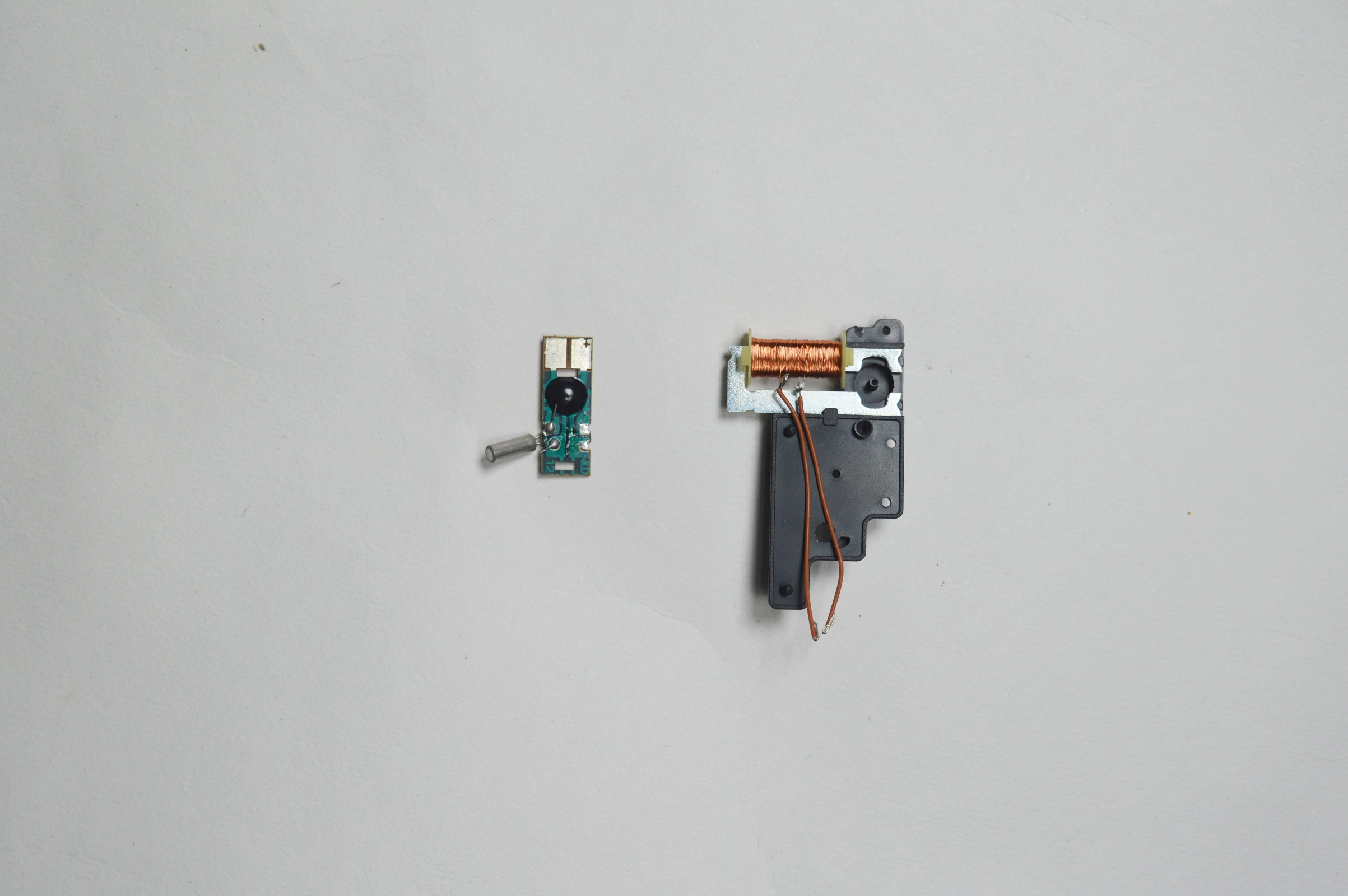
then a idea struck to my mind! Why don’t i take it apart (which i would have later anyway), and drive the motor with Box0!So first, i removed all the gear mechanism and made it to minimal so that the motor can work.
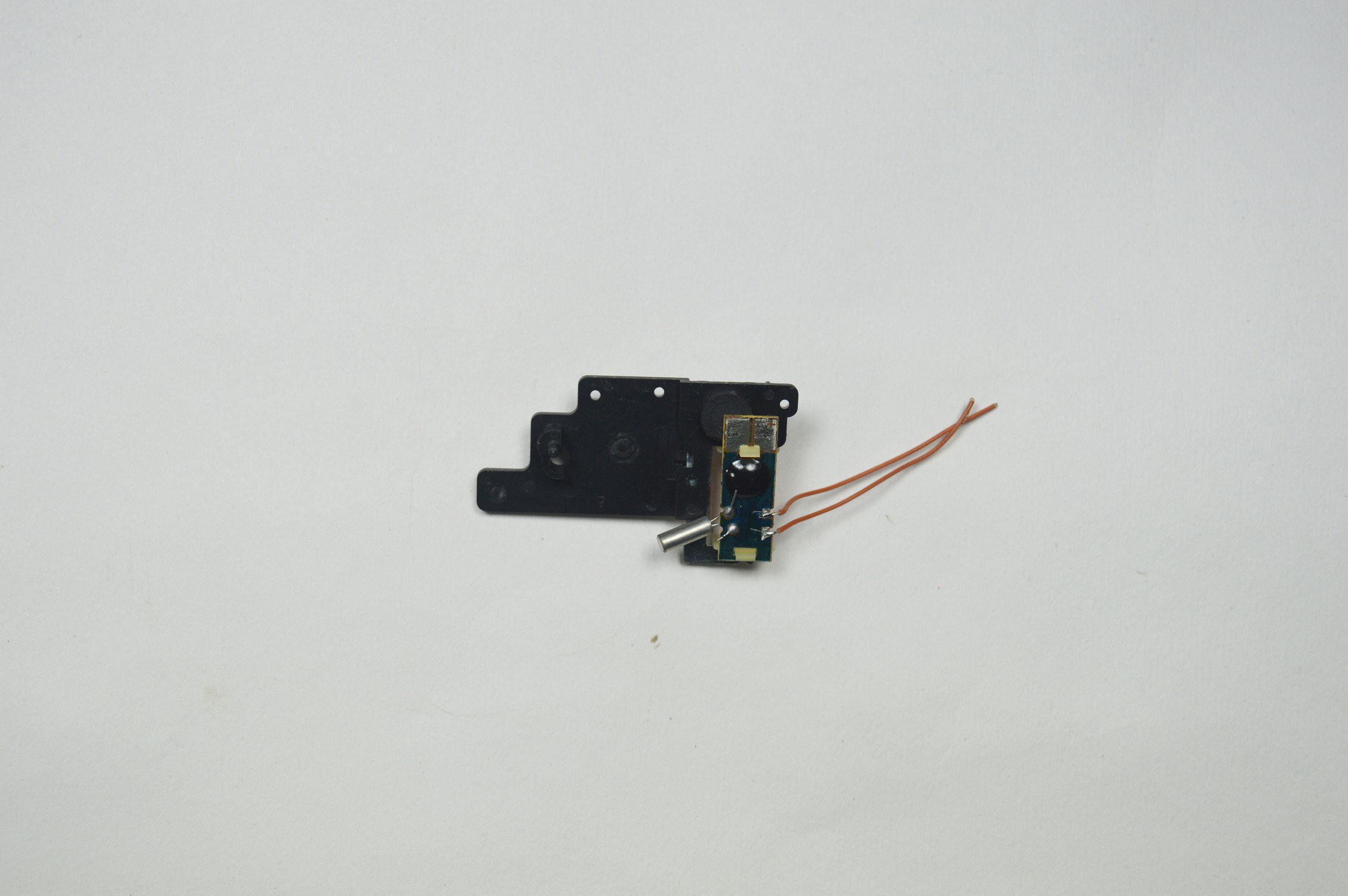
Now, the motor is functional, i soldered two wires to the coil solder pad (coming out of the IC underneath epoxy).![]()
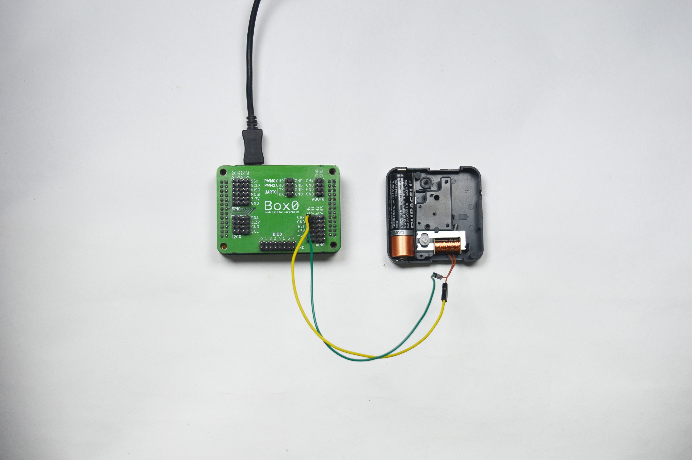
Attached the wires to Box0 (
AIN0.CH0andGNDpins) and started Box0 Studio – Oscilloscope to see the driving signal.![]()
![]()
![]()
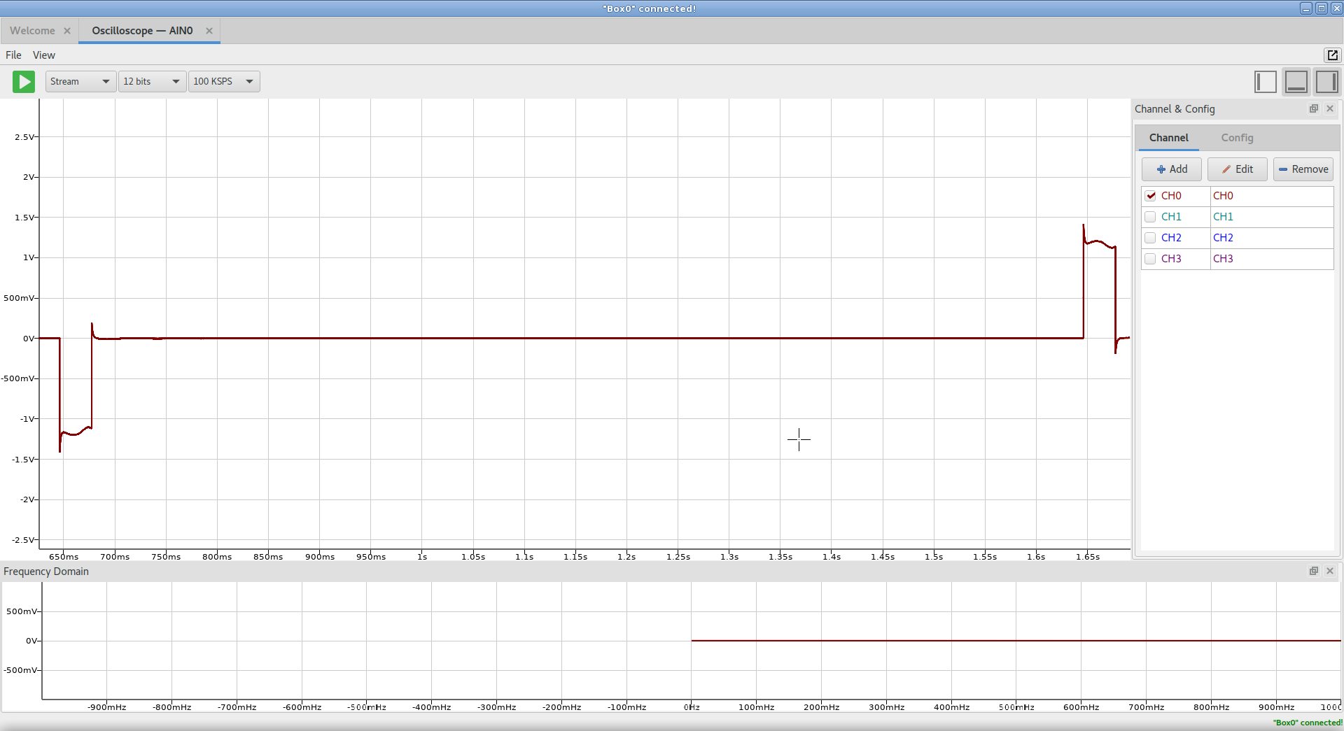
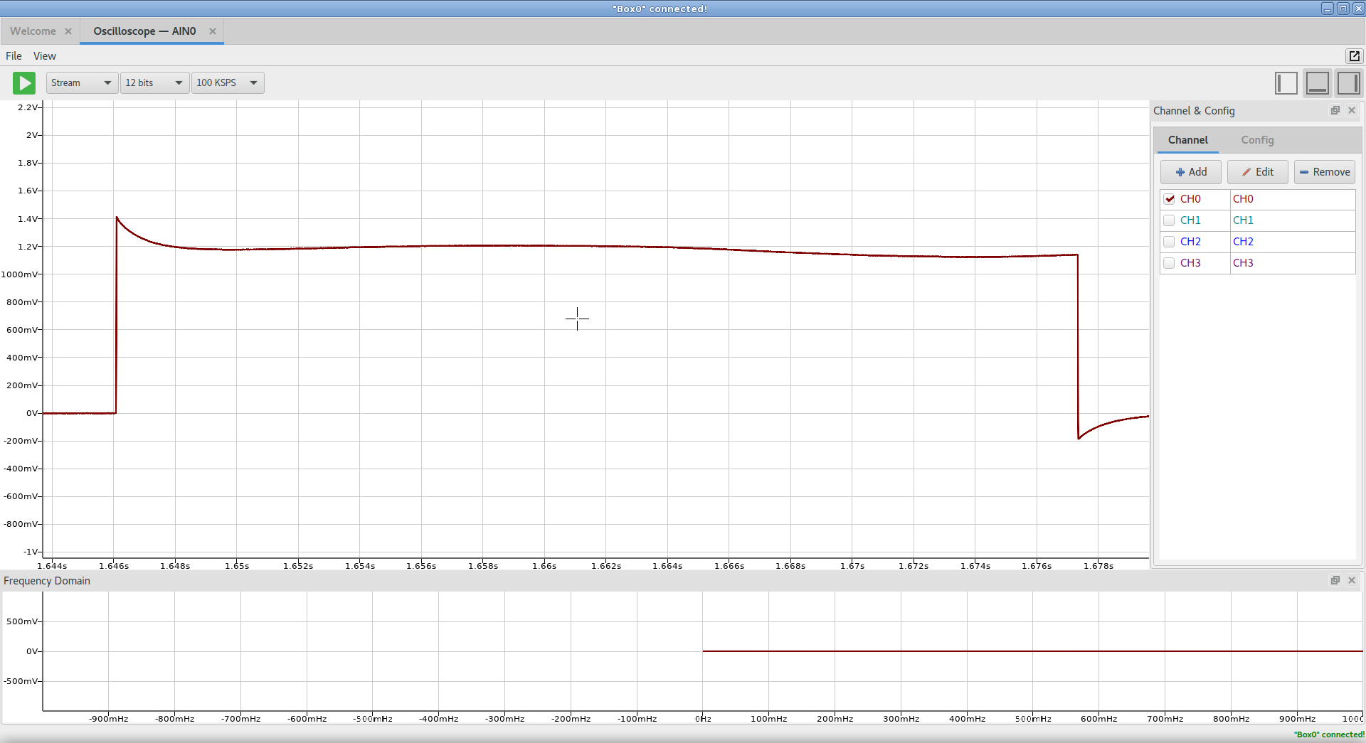
The signal is pretty simple (see video):
- generates a 32ms pulse with around +1.4V.
- wait 1 second (from the start of the pulse)
- generates a 32ms pulse with -1.4V
- wait 1 second (from the start of the pulse)
- goto “1”
Easy peasy, i can generate that signal with
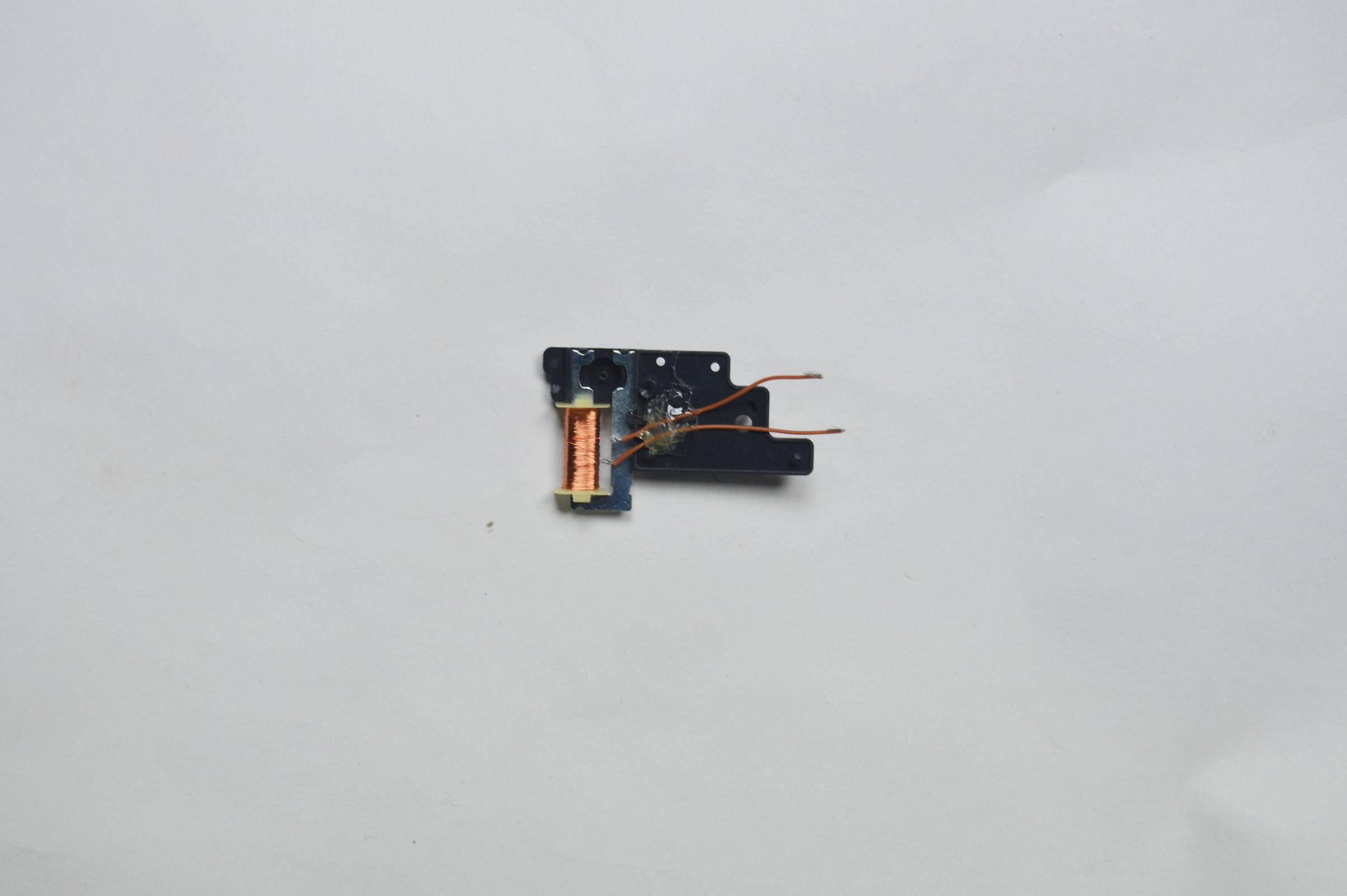
AOUT0(Analog OUT module of Box0).Now, with an idea about the signal, i completly removed the driver circuit.
![]()
And attached two wires to the coil copper wire, and connect them to Box0 (
AOUT0.CH0andGND).I glued the wire to body with glue gun so that copper wire don’t break.
![]()
Now, i wrote a little Python script, and it started working as expected!
Now, with able to drive the motor with Box0, i can start
abusing it ;)import box0 import numpy as np # python2 raw_input and python3 input try: input = raw_input except: pass # 10ms, 25ms (Demo 3 - Fastest) signal = np.empty(50) signal[:] = 0 signal[15:25] = 1.5 signal[40:50] = -1.5 SPEED = 1000 BITSIZE = 12 CHAN = 0 # Get resources dev = box0.usb.open_supported() aout = dev.aout() # output signal aout.snapshot_prepare() aout.bitsize_speed_set(BITSIZE, SPEED) aout.chan_seq_set([CHAN]) aout.snapshot_start(signal) input("Press any key to exit") # deallocate resources aout.snapshot_stop() del aout del devSo, i made multiple similar looking waveform, and i was able to control motor speed.
# 32ms, 1000ms (Demo 1 - Original)
#~ signal = np.empty(2000)
#~ signal[:] = 0
#~ signal[968:999] = 1.5
#~ signal[1968:1999] = -1.5

# 32ms, 500ms
#~ signal = np.empty(2000)
#~ signal[:] = 0
#~ signal[468:500] = 1.5
#~ signal[968:1000] = -1.5
#~ signal[1468:1500] = 1.5
#~ signal[1968:2000] = -1.5

# 20ms, 100ms (Demo 2)
#~ signal = np.empty(200)
#~ signal[:] = 0
#~ signal[80:100] = 1.5
#~ signal[180:200] = -1.5

# 20ms, 50ms
#~ signal = np.empty(100)
#~ signal[:] = 0
#~ signal[30:50] = 1.5
#~ signal[80:100] = -1.5

# 10ms, 25ms (Demo 3 - Fastest)
signal = np.empty(50)
signal[:] = 0
signal[15:25] = 1.5
signal[40:50] = -1.5
Here you have!
- a seamingly useless little clock motor get to see another day!
- I found the puppy.:)
Btw,
Before actually driving the motor withAOUT0.CH0, i connectedAOUT0.CH0->AIN0.CH0pin, and checked if im not generating a faulty signal.
Thanks to the modular architecture of Box0, i was able to runAOUT0module with Python code andAIN0with Box0 Studio – Oscilloscope.Note: All above code under GPLv3+
Originally posted on: https://madresistor.com/blog/hacking-wall-clock-box0/
-
Beta testing update!
01/20/2017 at 15:18 • 0 comments![]()
Last week we announced Box0 beta testing on Hackaday and assembled a few boards for the same.
We are looking for awesome people who are interested in making some projects or perform experiment/activity with Box0 and document them.
The software is working nicely on GNU/Linux and has been tested with Arch and Ubuntu though things are a bit sluggish on Microsoft Windows 10.
Its not a hard core requirement but initally we are mostly looking for people who are comfortable with using GNU/Linux and also understand a
bit of programming, electronics and compiling source code. Even if you are a beginner but still interested then we are there to help you :)
You can use Ubuntu as your OS which is considered friendly for beginners.All your contributions in form of tutorials, schematics, code and other material will be completely attributed to you.
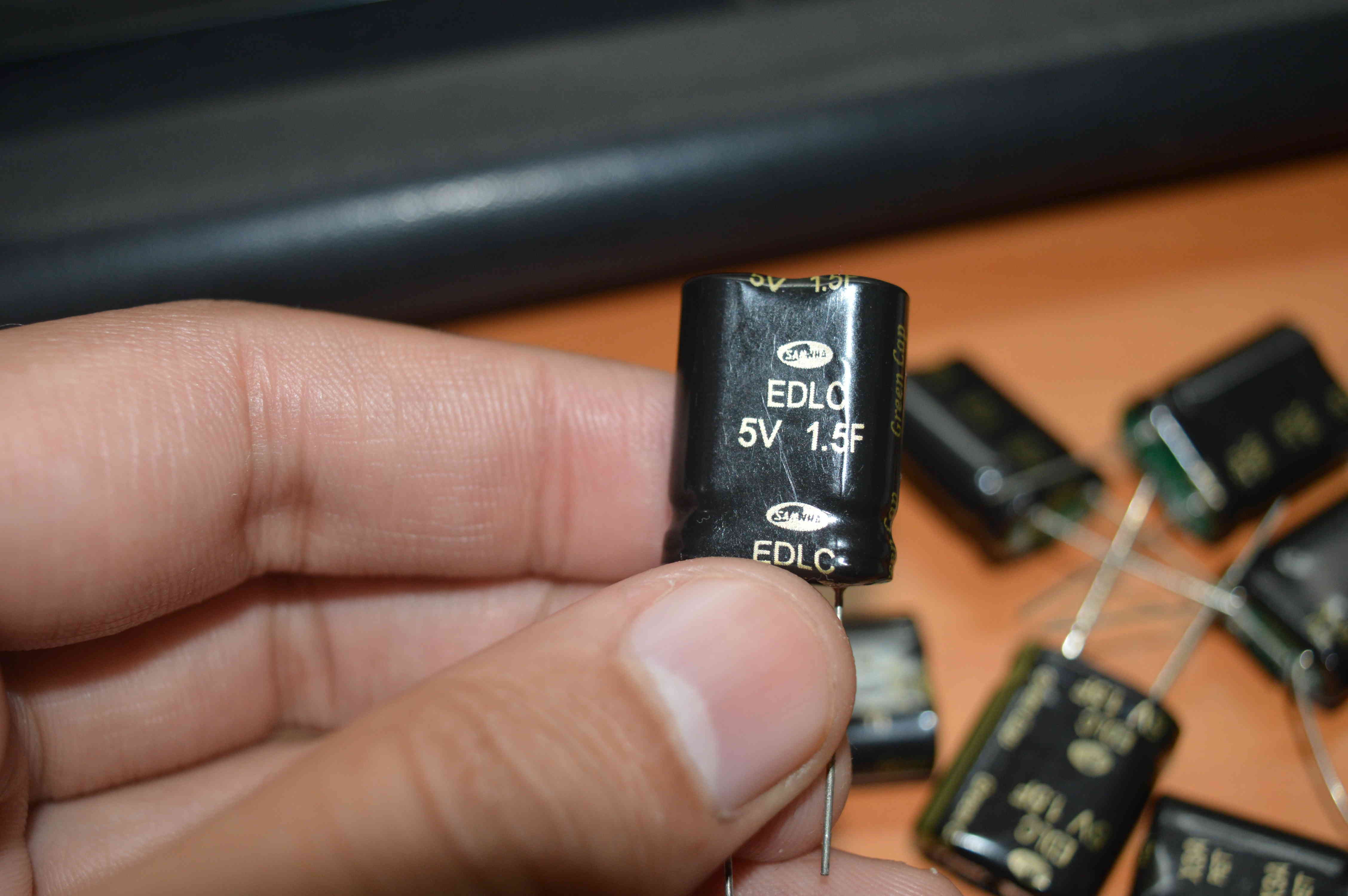
We just want community work to be available under free/libre/open-source licence for others.We are also sending a 1.5 Farad super capacitors to all the beta testers as a new years gift so they can try some weird stuff with them :}
If you would like to know anything more come over and say hi on #madresistor at IRC Freenode or drop us an e-mail at contact@madresistor.com.
![]()
Originally posted on: https://madresistor.com/blog/box0-beta-testing/
-
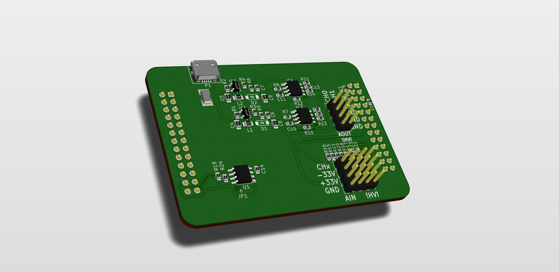
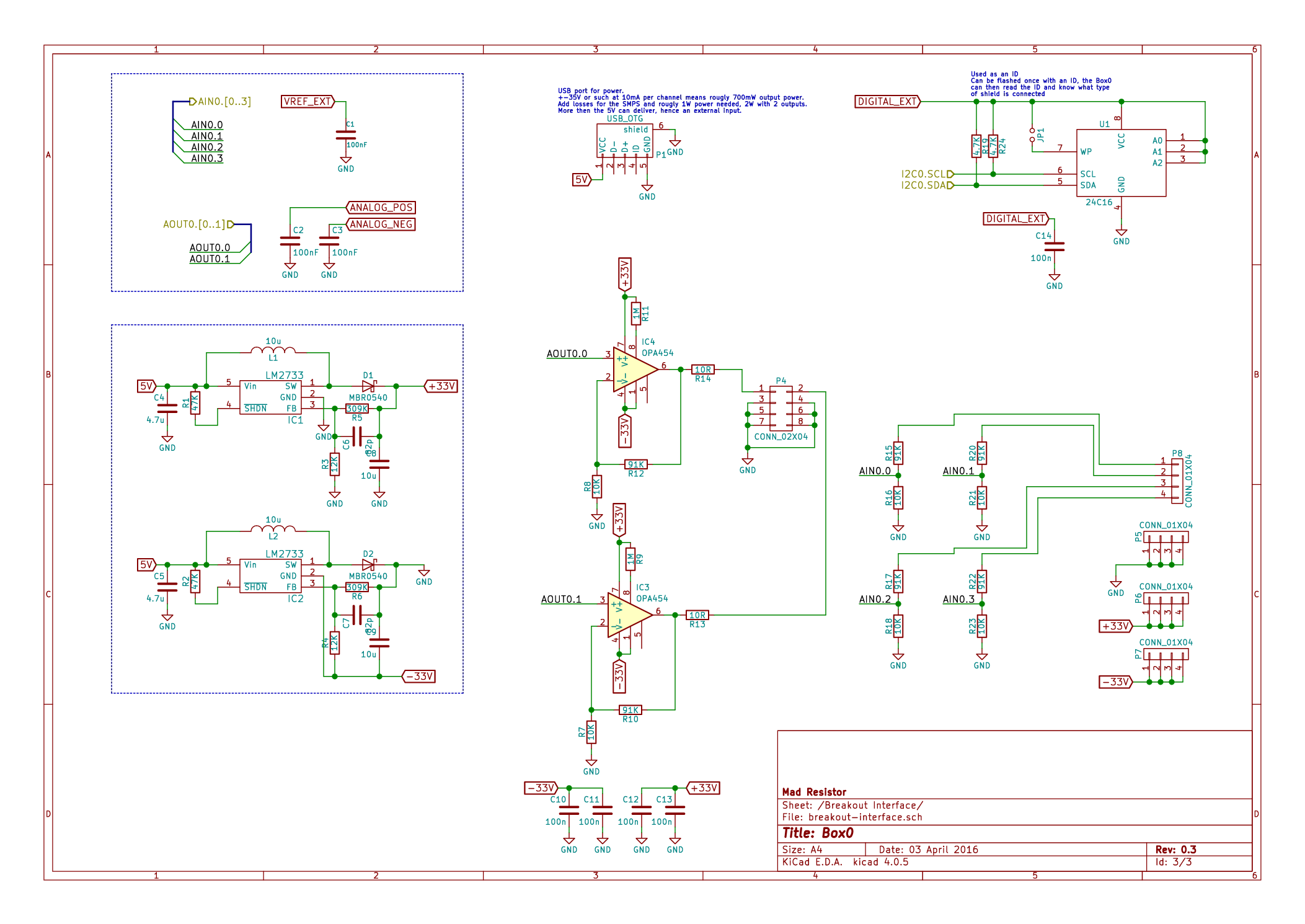
High voltage analog IO for Box0
01/12/2017 at 12:34 • 0 commentsSurprise! We have something to show you :)
Recently, [Ferix] (one of our beta tester) shared hardware design of Box0 shield on his github Repository.
![]()
![]()
[Ferix] writes:
A breakout board for the Box0 so the Box0 is able to handle higher analog voltages With this it can handle -33 to +33V on the input and output -33V to +33V as well.

The hardware is simple, 2 switching power supplies to boost the 5V in to +-33V, possible +-35V After that 2 +-50V 50mA output capable opamps with a gain of 10 and a divide by 10 voltage devider so the analog inputs can handle +-33V as well

An USB port is added to supply the board with 5V as the 5V pin of the Box0 is unable to deliver enough current. A small example:

10mA at 35V means that, at 100% efficiency, 70mA is needed at 5V, in practise this figure is closer to 90mA With 2 opamps being capable of delivering 50mA a total of 100mA at 35V is required, meaning 900mA at 5V as input.

Current limit is implemented by using a 1A polyfuse, minimal but better then nothing.
His design is lm2733 for generating +33V and -33V for Analog out OpAmp’s.
And using voltage divider for analog in.He is using an USB micro for more power.
[Ferix] has used KiCAD (Free/Open source PCB designing software) for designing his PCB.
What is on your mind?
You can install KiCAD, download Ferix repo, tweak the design for your needs, get it manufactured and do something wonderful – let us know what you did :)
You will also need a Box0 for using [Ferix] shield, for which you can sign up for the crowdfunding campign or get a beta tester board by contacting us at contact@madresistor.com.We will write a follow up post when [Ferix] get the design into reality and share what he is upto!
Originally posted on: https://madresistor.com/blog/high-voltage-analog-box0/
-
Arch AUR packages for Box0!
01/08/2017 at 01:44 • 0 commentsLooking for Arch GNU/Linux package for Box0?
See: Arch AUR package listYou can install the packages using AUR package installer like, pacaur.
$ pacaur -S libbox0-git lmfit-git libreplot-git
 $ pacaur -S box0-studio-qt-git liab-studio-qt-git box0-utils-git
Note: The two command need to execute in the order as above.
-
Box0 - 3D printed enclosure (prototype)
09/30/2016 at 07:21 • 0 comments![]()
![]()
In the second run, we will improve the design and
will be commit the design files to box0-v5 repo. stay tuned!
Made using OpenSCAD.
Thanks to folks at Meerut Maker Space!
-
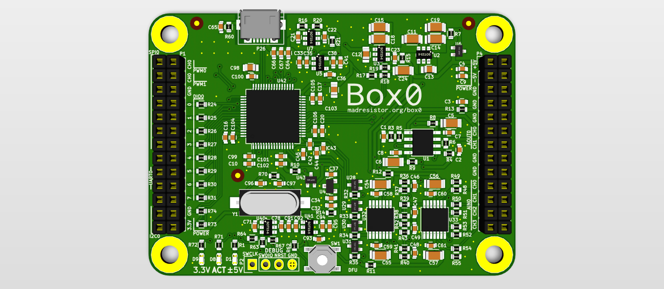
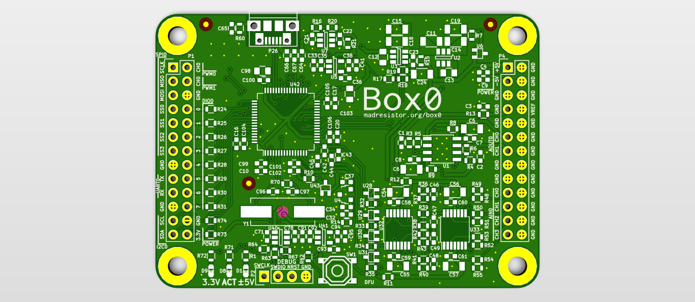
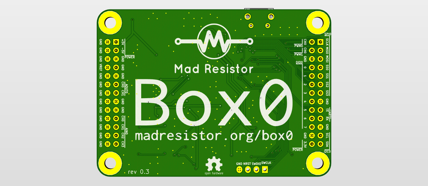
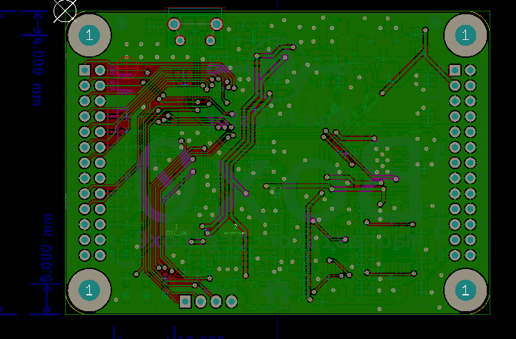
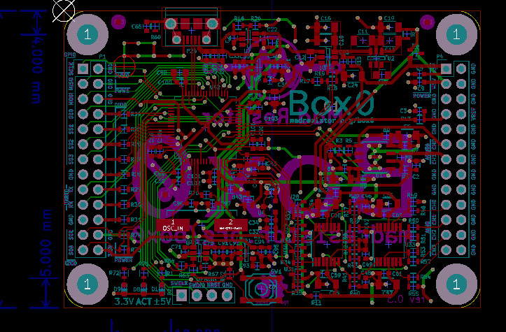
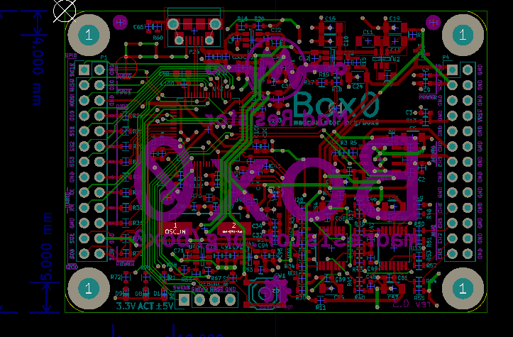
PCB (& 3D) ride!
09/21/2016 at 00:55 • 0 comments![3D Top - with components]()
3D Top - with components (computer generated)
![3D Top - without components]()
3D Top - without components (computer generated)
![]() 3D Back - with components (computer generated)
3D Back - with components (computer generated)![Filled Top]()
Filled Top
![Filled Back]()
Filled Back
![Unfilled Top]()
Unfilled Top
![Unfilled Back]()
Unfilled Back
You get the KiCad files from git repo here.
2 Layer design, while designing, it was a goose chase to get the right position and connection!
In the charge pump (-5V from +5V) block [and other power management block]:
Special care have been taken to reduce the loop (high current path). by using Via and minimal cut in ground plain.
To make the connector even more stronger, we placed copper under it.
So that the connector can get even more strength from the solder.
-
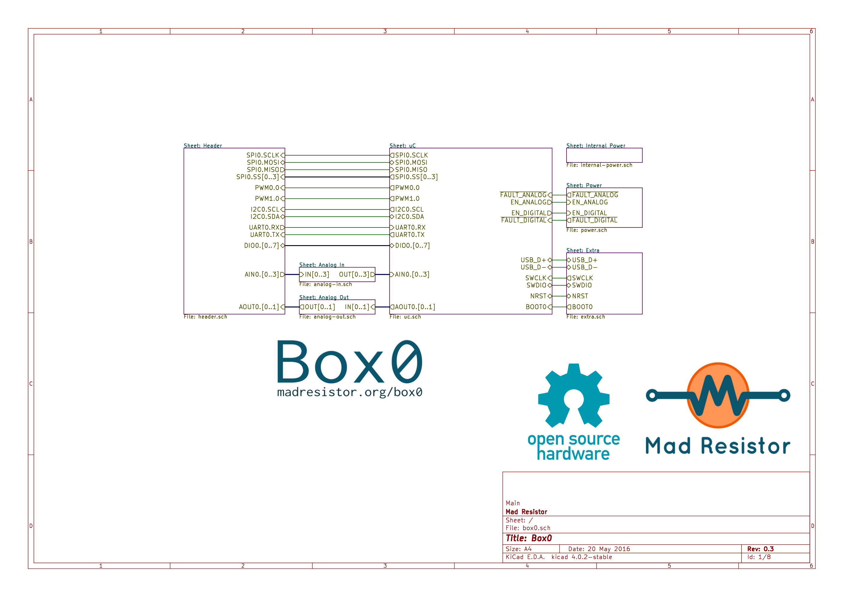
Schematic ride!
09/20/2016 at 20:01 • 0 comments![]() Click on image for higher resolution.
Click on image for higher resolution.(For complete schematic in PDF click here)
The first sheet contains a high level overview of the schematics.
The design has been divided into different subsystems which interact with each other in an abstract manner.The schematic for these subsystems has been put in their respective sheets.This helps to reduce the clutter, provides better design management, ease of readability and usability.
We will explain a bit about different subsystems one by one to help you get an idea.
Sheet: uC![]()
This block mainly does the following
- Communication (USB, SPI, I2C...)
- Control and coordination of power management ICs
- ADC input and DAC output.
- Digital input and output
Top Left: The microcontroller STM32F072 - ARM Cortex M0.- USB FS (12Mbit)
- ADC 1MSPS, 12 bit
- DAC 1MSPS, 12 bit
- DMA 7 channel
- I2C upto 400Khz
- SPI upto 36MHz
- CAN
- Alot more, see full specification.
Top Right: Proper power supply decoupling and bypassing capacitors for analog and digital parts of microcontroller as per recommendations in datasheet.Top Right extreme corner: if you noticed there is a schottky diode BAT54SW connected between VDDA and VDD of the uC to make sure the potential difference between both the pins remains within safe limit (mainly during startup when power supplies are from different sources, fro e.g when the optional voltage reference for VDDA is used on Box0)
Bottom Left: These are led for activity, power, power-fault indication.
Middle Right: Various pins of microcontroller connected/named/converted according to Box0 pins specification.
Bottom Middle: The list of DMA channel, Timers used for which task and which peripherial pins are being used for what purpose.
At bottom and right to the led is the crystal oscillator for a clean and stable (10-30 PPM)clock signal to the microcontroller.This works well for our requirements.Though the microcontroller has a RC oscillator built-in but it is no match for a good crystal.
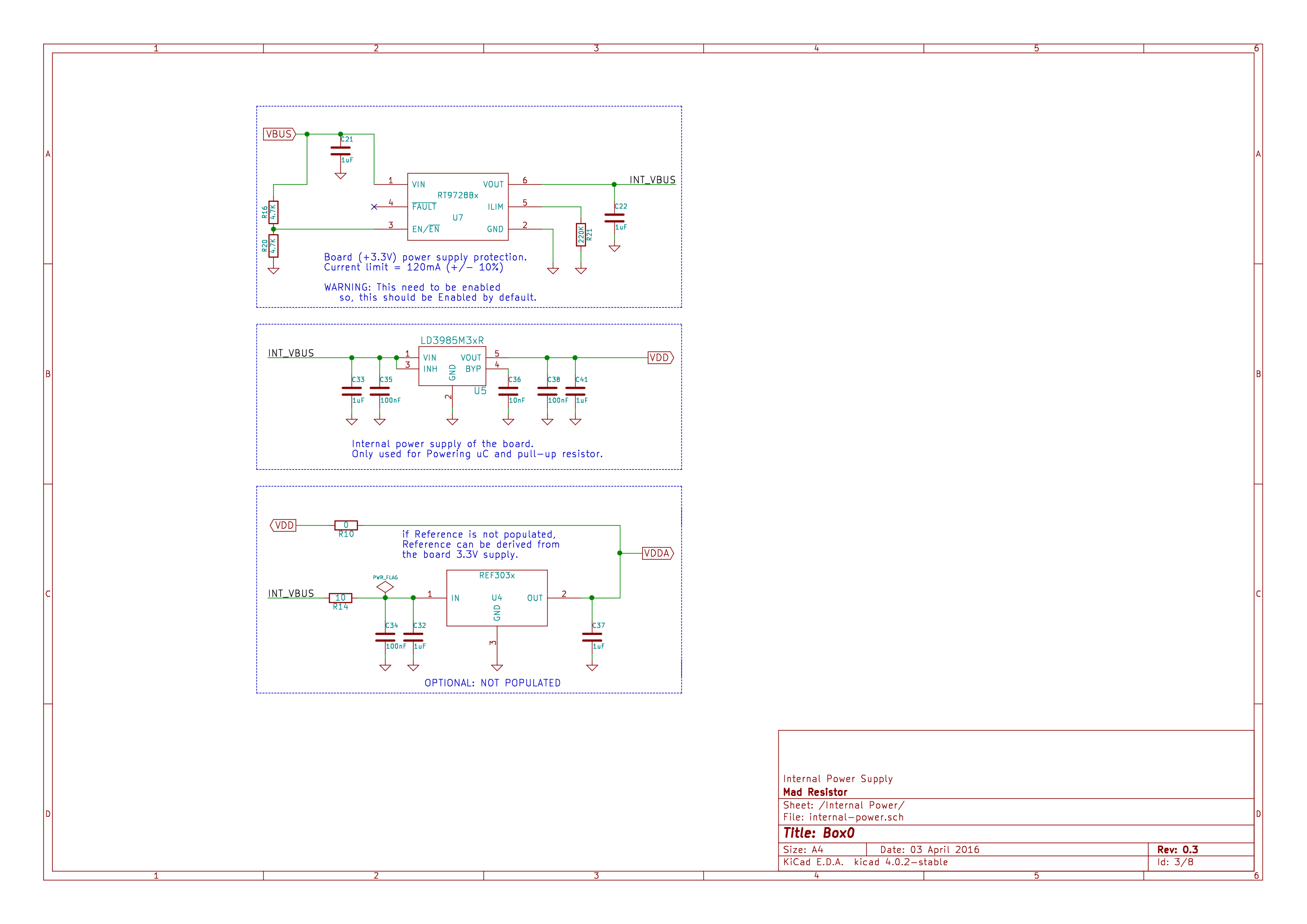
Sheet: Internal power![]()
Box0 consist dedicated power supplies for internal and external use.
The internal power supply sheet consist of power managements parts to power the board components only (includes microcontroller).
The power supply automatically turns itself off in case of short circuit or if the current limit exceeds above a certain programmed level.Top box: RT9728 for active current limit on power coming from USB (in case something bad goes on the board).
Middle box: a 3.3V regulator
Bottom box: a 3.3V [optional] precision reference.
If the precision reference is not populated, it can be connected to the above 3.3V voltage regulator.
The (virtual) power output from this sheet is not provided to user (ie external use).
(except - precision reference which can be used for external use too via "VREF" pin which at the output of which a resistance is placed to limit the currents to safe level during accidental shorts circuits by the user)
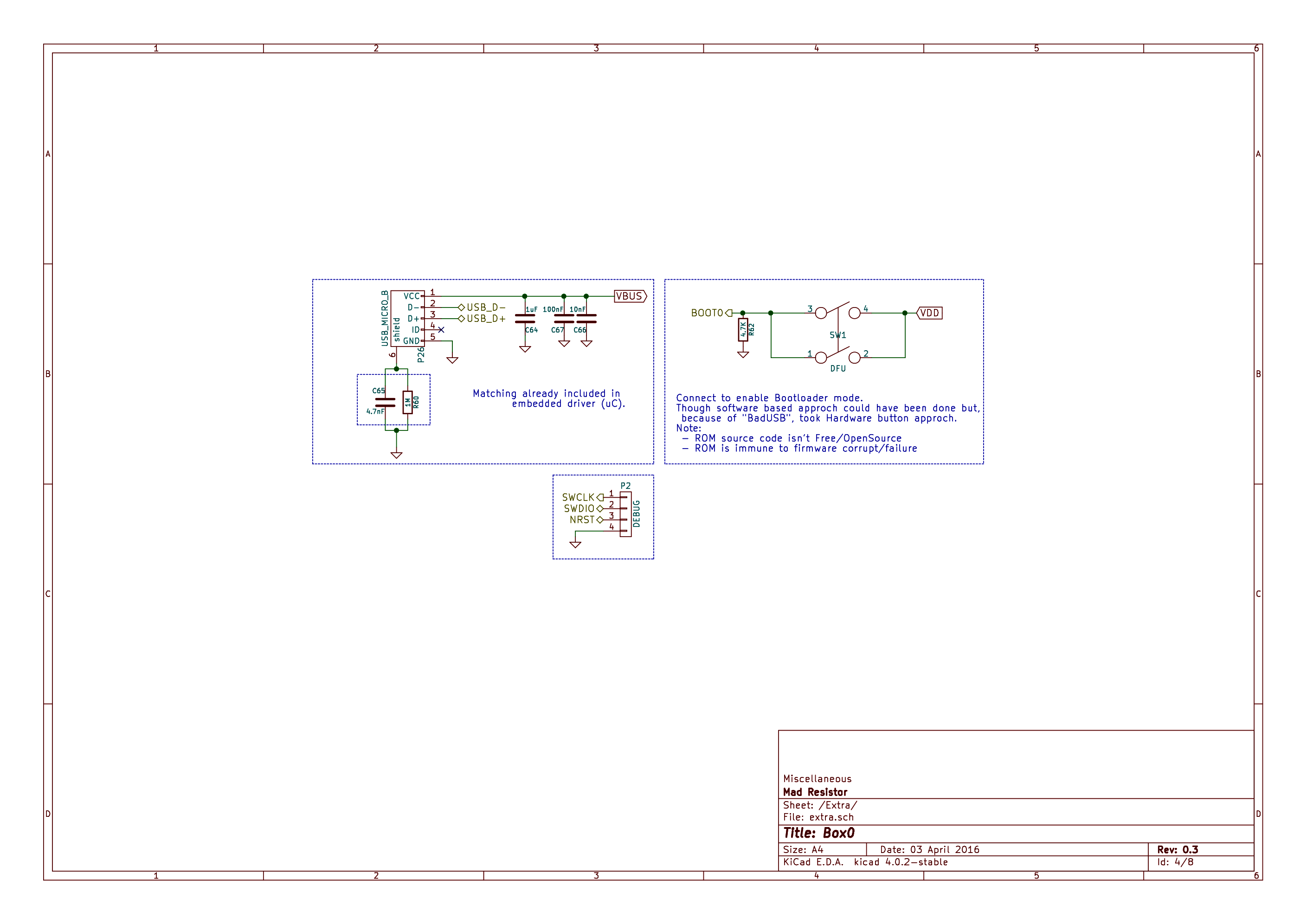
Sheet: Extra![]()
The USB connector, debug pin (SWD) and the BOOT0 (for DFU) button.
Special story for BOOT0 button:
If you are familiar with BadUSB which has also been documented by hackaday here (which @Kuldeep Singh Dhaka tipped off ;).
In order to prevent BadUSB, the BOOT0 button is placed.
When user press the button, the device boot from ROM (proprietary* code by ST).
When it boot from ROM it comes up as a DFU device (USB DFU class - Device Firmware Update).
Only the firmware can be updated when the user want to. There is no possibility of automatic firmware update which do not fullfill the BadUSB requirement.
and btw, if someone can flash malice code to your device, they can do more nasty things.
* = though the ROM is proprietary, just trade-off.
In future we can implement the functionality via flash code.
Also, we can even start a full-fledged project that allow [same flashing api, multiple vendor support] for ARM microcontroller - something like UBOOT for microcontroller ;).
future is bright, lets see!
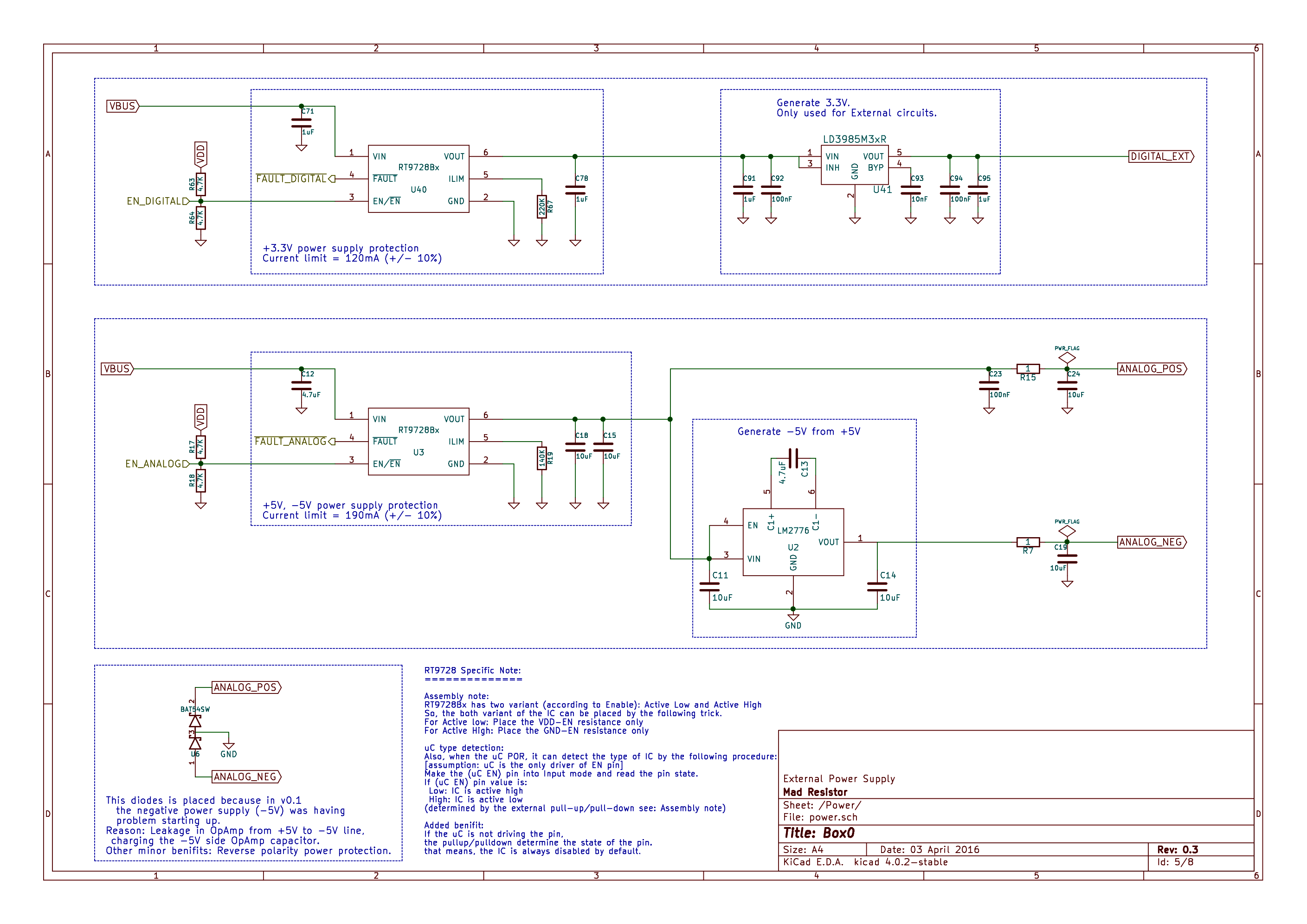
Sheet: Power![]()
Having onboard short circuit protected and commonly used 3.3V , +5V, -5V is a very helpful for the user while prototyping different type of analog and digital circuits.The power supplies are also quite usable in terms of noise level and current output.
- +5V - active current limit
- -5V - active current limit
- +3.3V - active current limit
In case, the RT9728 current* exceed an interrupt is generated for microcontroller.
* = current limit is set by resistance
Note: The +5V and -5V is also used for powering on board OpAmp's. trade-off because placing another +5V, -5V circuit was costly.Practically its a good tradeoff and we never faced any issues in usability.
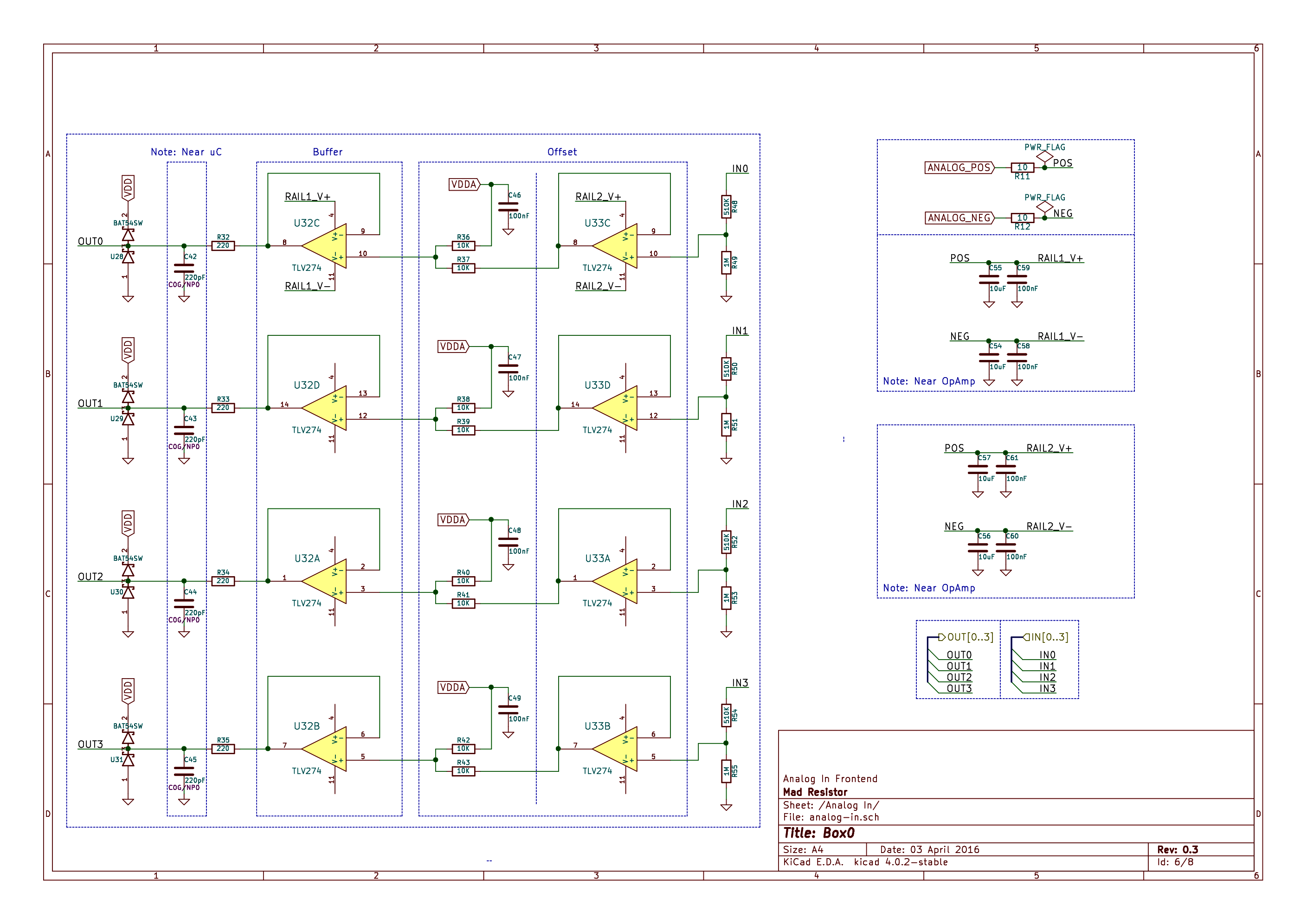
Sheet: Analog In![]() Aim: Condition the external bipolar signal (input range depend upon the ratio of voltage divider) signal to fit the acceptable level of 0V to +3.3V of the internal SAR ADC or micro controller.
Aim: Condition the external bipolar signal (input range depend upon the ratio of voltage divider) signal to fit the acceptable level of 0V to +3.3V of the internal SAR ADC or micro controller.Basically: Input-> divide -> buffer -> offset -> buffer->filter->over voltage protect-> feed to ADC input.
We are using TL274 Opamps from Texas instruments.
These have very high input impedance and almost negligible input bias current and has rail to rail o/p capability along with low power consumption.The bandwidth and slew rate suffice for our purpose for feeding the SAR ADC sampling rate.
Also, if you noticed, there four capacitors used in the RC filter which is connected to the opamp output just before the ADC inputs.
These are Class I dielectric "C0G/NP0" capacitors which do not distort the signal quality as compared to other dielectrics such as X7R or X5R whose capacitance varies with applied voltage.
These capacitors work to filter the input signal to the SAR ADC and also work as charge storage for proper sampling of the SAR ADC thus isolating the the opamp output from the transient caused by the input sampling circuit phenomenon.Also these capacitors absorbs the charge
capacitor on each OpAmp output pin. Specially designated with "C0G/NP0". These are 1st class dilectric special capacitors and offers very low distortion as compared to other ceramic capacitors.Everyone learned from physics text books that capacitance depends on geometry.
Engineering side: capacitance can depend on other factors too : temperature, boasing voltage.
Generally available capacitors have different capacitance at different voltages. (ie capacitance is a function of voltage too).
So, when a heigher voltage signal comes in, capacitance varies, and charging behaviour changes, so the signal is also affected - final: distorts the signals.
Similar type of "COG/NP0" capacitors are also used for crystals (see: microcontroller subsheet) in this case primarily because these capacitors are quite stable with temperature and has good long term stability.
![]()
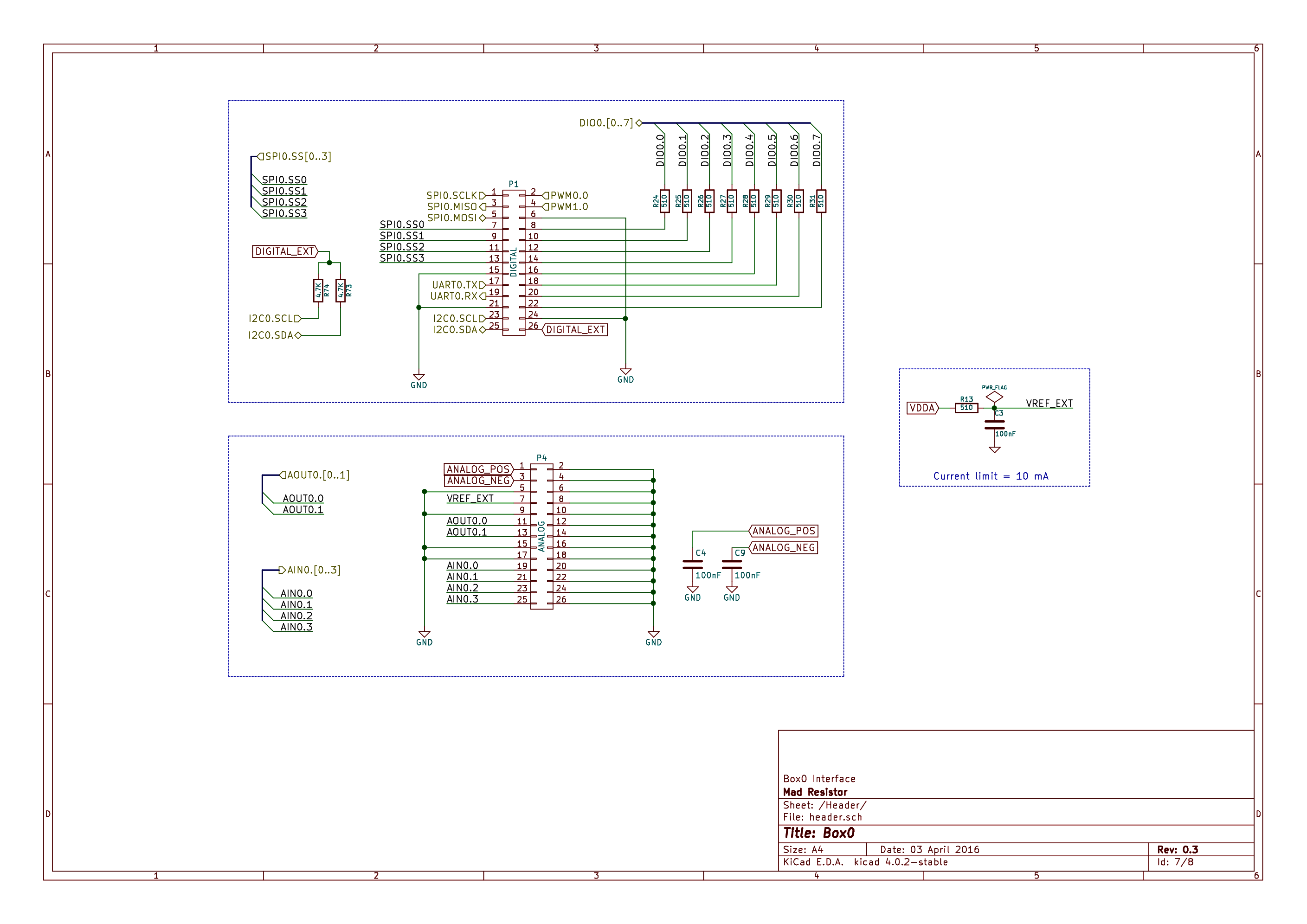
The pin headers for interfacing box0-v5 compatible shields.
- Current limiting resistance for microcontroller pin (as "DIO0" pins).
- I2C bus pull-up
- Current limit resistance for voltage precision reference ("VREF" pin)
![]()
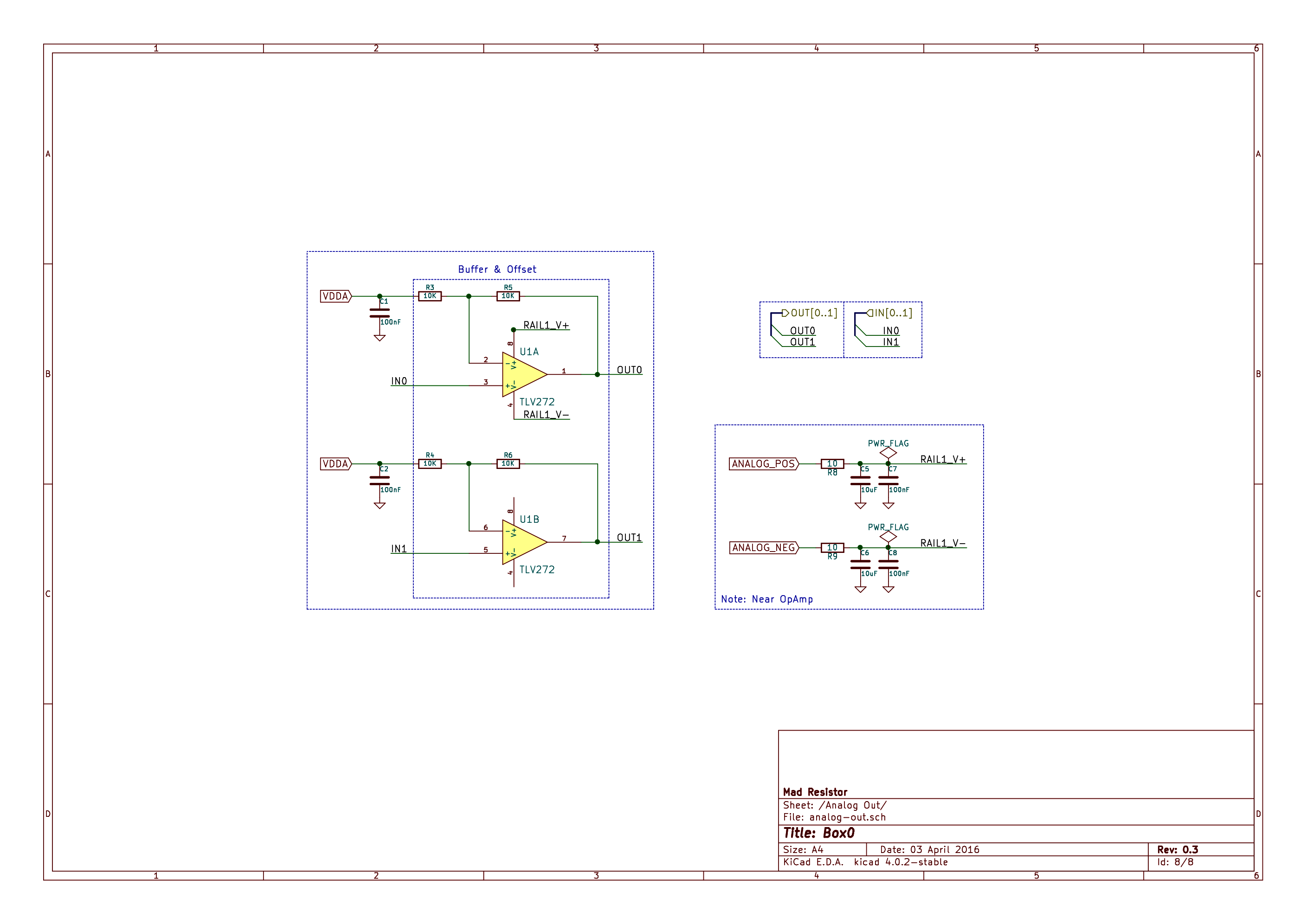
Analog output subsheet.
Aim: Convert 0V to 3.3V to -3.3V to +3.3V.
basically: Offset -> Buffer.
The opamps used is TLV272 in a SOIC8 package which works well for heat dissipaition from the amplifers.These Opamps have in impedance CMOS inputs, low input offset voltage and good output drive capability(much better than the generic jellybean - LM358).
This document be updated in future with more details when we will have some free time. -
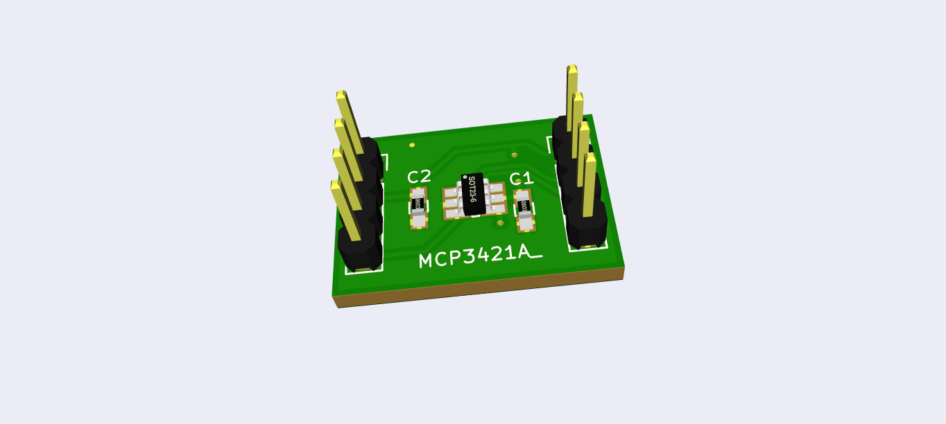
MCP3421-low cost 18 bits delta sigma ADC
07/10/2016 at 18:19 • 0 comments![]()
-
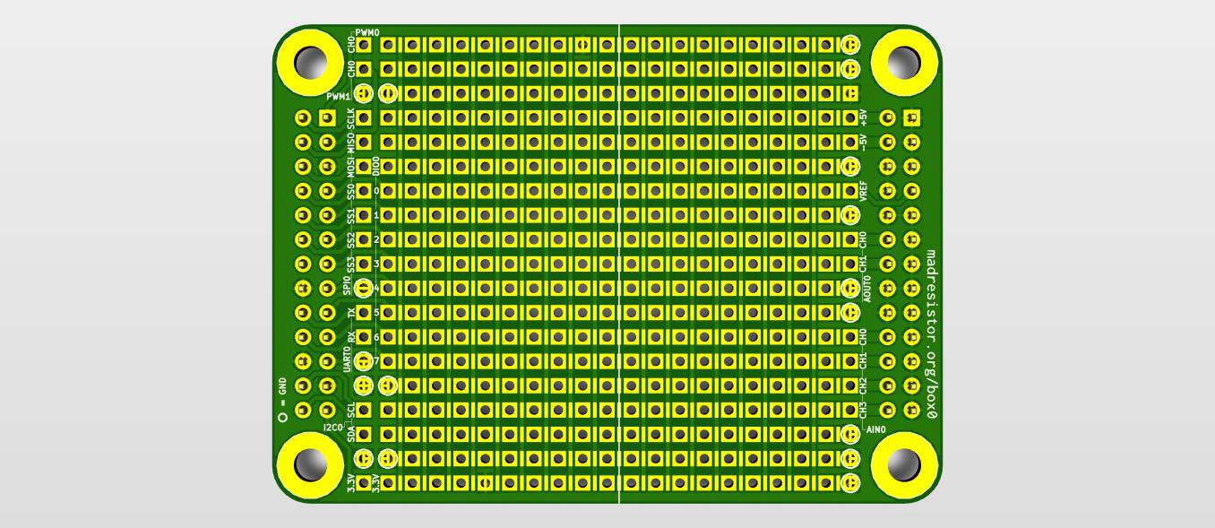
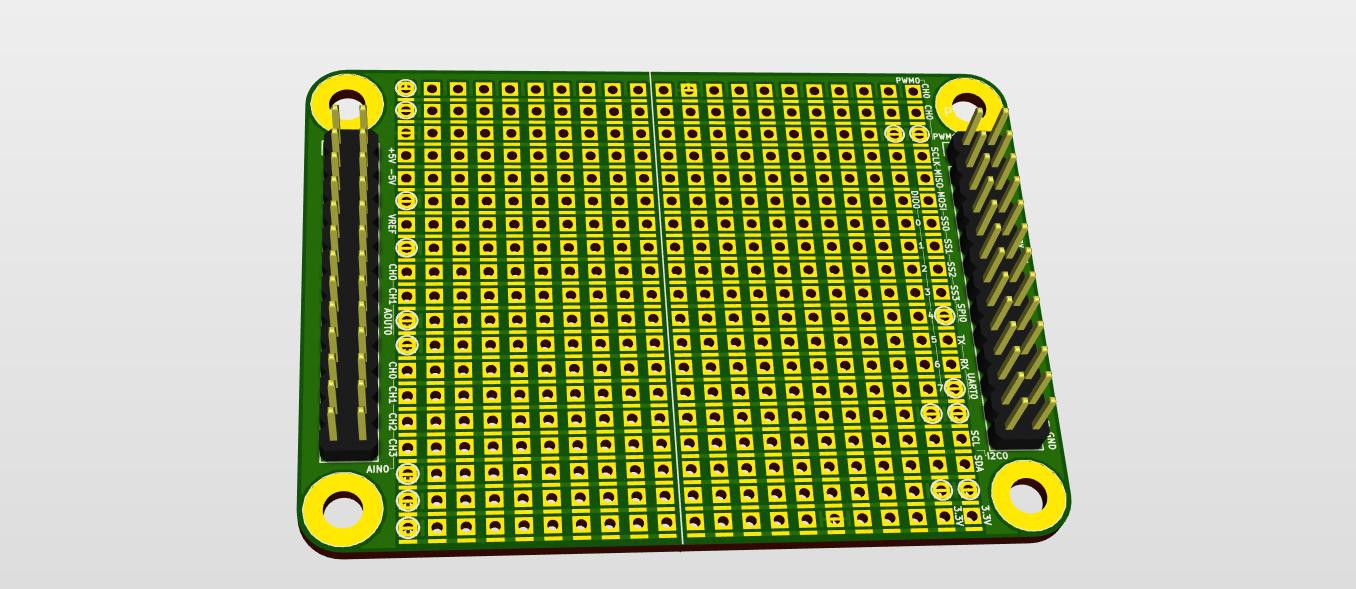
Millo - Proto board type II for DIY projects
07/10/2016 at 18:11 • 0 comments![]()
![]()
The board is an outcome of "Box0 intrument interface" + "Perf+"
(the vertical-track[on-front] / horizontal-track[on-back] between drill is of Perf+)
You can read more on Perf+ here http://hackaday.com/2016/06/16/evaluating-the-unusual-and-innovative-perf-protoboard/
Box0
Free and open source tool for exploring science and electronics anytime anywhere

 3D Back - with components (computer generated)
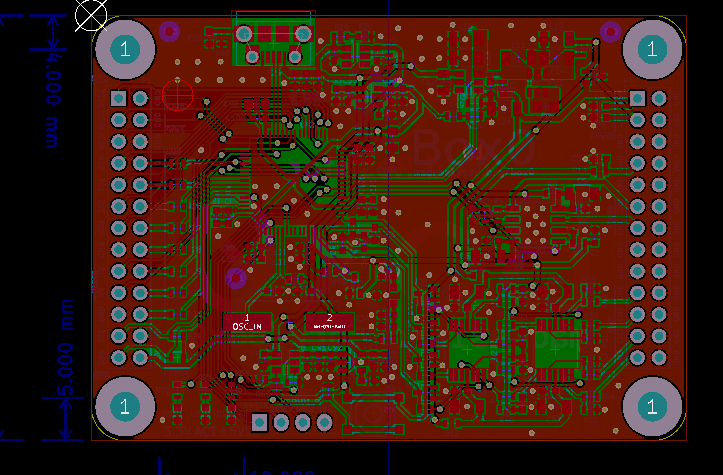
 Click on image for higher resolution.
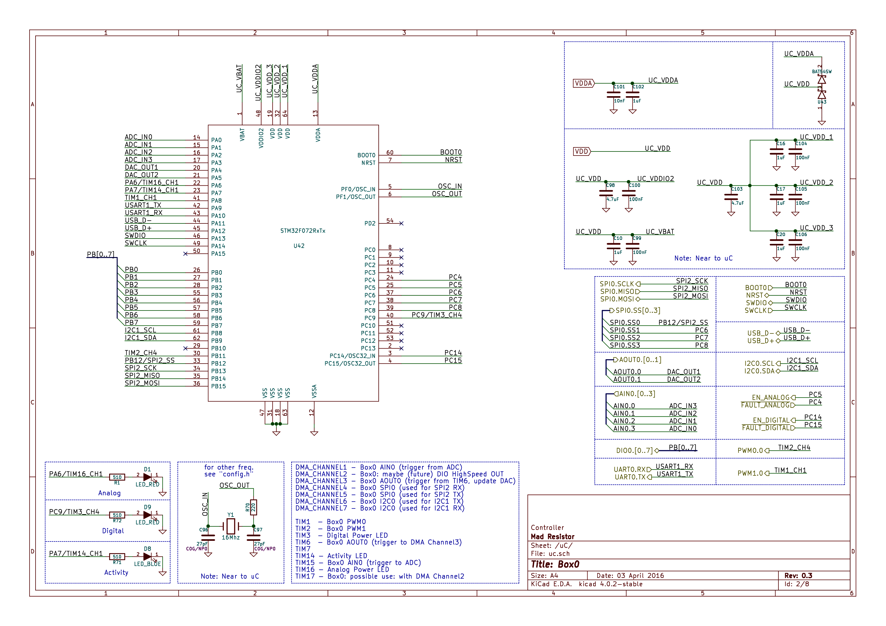
 Aim: Condition the external bipolar signal (input range depend upon the ratio of voltage divider) signal to fit the acceptable level of 0V to +3.3V of the internal SAR ADC or micro controller.