Germanium Vision
Low-resolution video camera with a lot of opened germanium transistors used as light-sensitive elements
Low-resolution video camera with a lot of opened germanium transistors used as light-sensitive elements
To make the experience fit your profile, pick a username and tell us what interests you.
We found and based on your interests.
For this project I've got a few flat lenses (Fresnel):
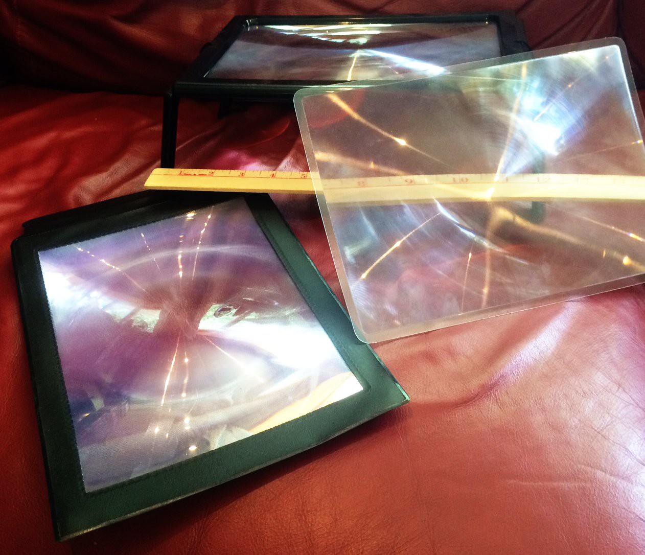
And largest one is 11x7.5 inches (not pictured here), so if one "open transistor cell" will occupy area 0.5x0.5 inches then I can achieve enormous image resolution 22x15 pixels!
Project got covered by hackaday.com!
http://hackaday.com/2016/06/03/hackaday-prize-entry-germanium-vision/
Thank you editors of Hackaday! ;)
Now we can try to use it as phototransistor as per this soviet book from my childhood (1st schematics):
I took МП25А (MP25A) and built 1st stage of that circuit on the breadboard:
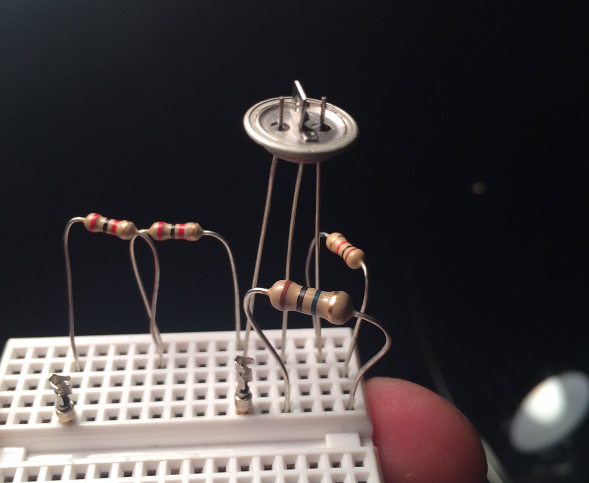
R1 and R2 were represented by single resistor 1M (and instead of R3 it was series of 2K resistors, because I didn't have 5.1K right away). Voltmeter showed slightly under 1V between emitter and ground (which should be positive for P-N-P transistors) in the dark and above 2V on the bright light.
Better transistors like МР42А (MP42A) could be used as solar cell to generate voltage directly!
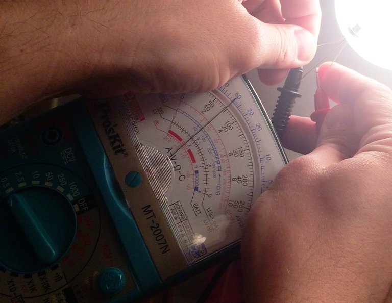
Here you can see 0.15V between base (negative) and collector (similar results fro emitter).
P.S. I also remembered this trick from childhood - article about solar panel from transistors was published by one soviet magazine for kids in early 80s:
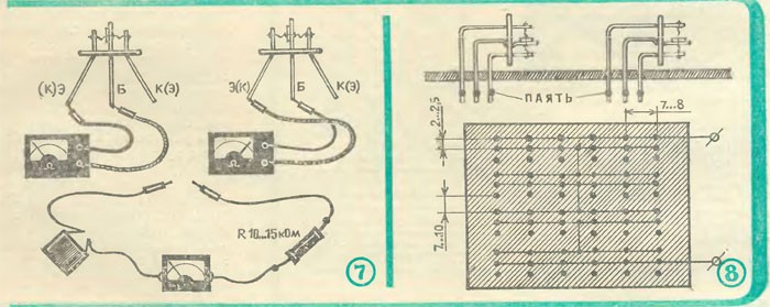
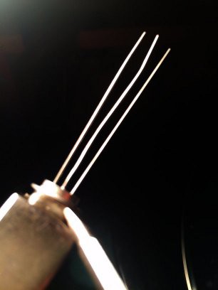
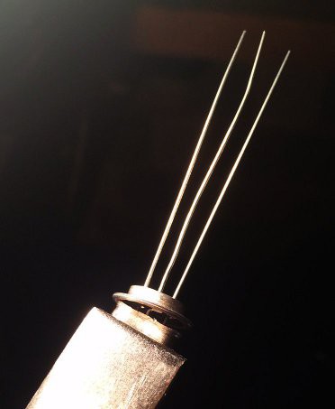
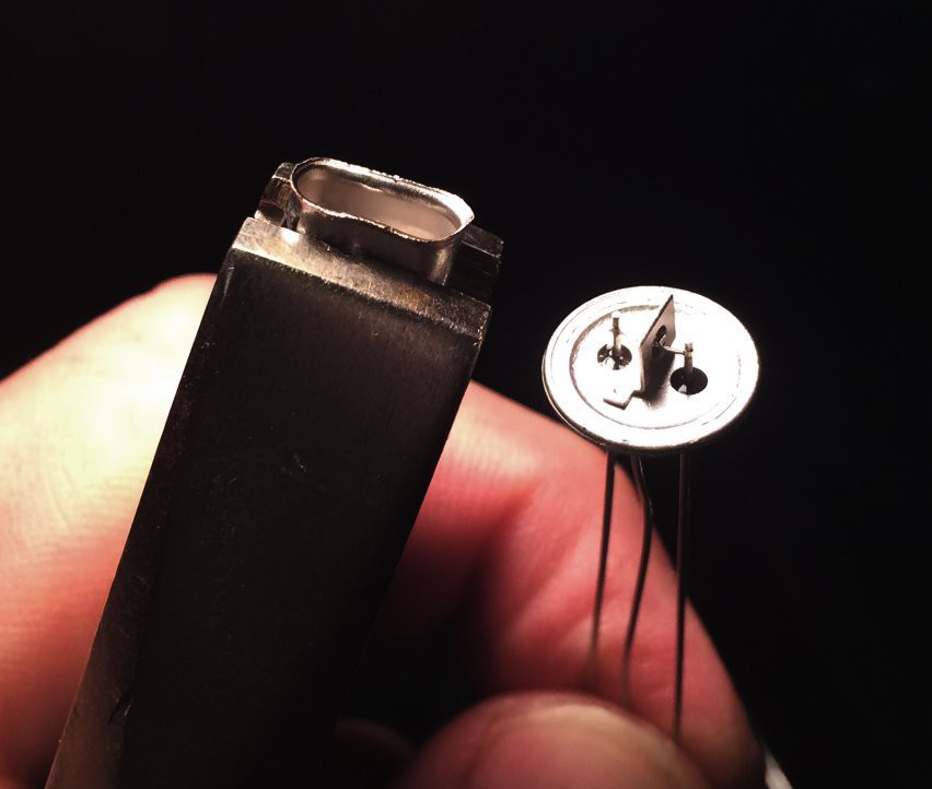
Soviet MP-transistors are relatively easy to open:
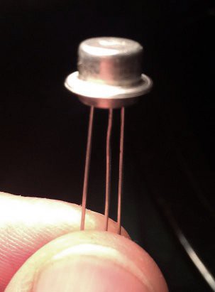
First of all you need pliers to hold a head of transistor like this to avoid damaging of semiconductor joints inside:
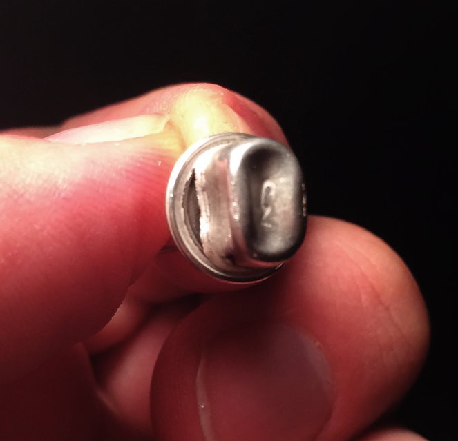
Then you need to squeeze the head to break it:
Create an account to leave a comment. Already have an account? Log In.
Одна из проблем с германием — большие темновые токи и их сильная зависимость от температуры. Тоже пытался как-то сделать простой фотодетектор на основе германиевого транзистора, но стабильной работы добиться не удалось. С кремниевыми фототранзисторами результаты были гораздо лучше.
Drawbacks of germanium include higher dark currents, with strong temperature dependence. My previous attempts at making a simple photodetector on the basis of a germanium transistor failed to produce consistent results. A silicon phototransistor performed much better.
Я сконцентрируюсь на германии и потом товарищ чуть ниже пишет, что порог срабатывания у германия чуть ниже, чем у кремния :)
I make my own alpha detectors by uncapping transistors and applying the particles directly to the base-emitter junction. This works for older power transistors (2N3055) as well as small signal 2N2222. (With an appropriate amplifier you can detect individual particles, including heavy particles (muons?) from cosmic rays.)
I've found a good way to decap the smaller 2N2222 transistors is to clamp them by their head (wires hanging down down) in a drill press and apply a file to the outside while spinning. Eventually the file breaks through and the uncapped transistor will fall into your hand.
Per the document link below, the energy per charge carrier of silicon is 3.62 eV, and for germanium it is 2.96 eV. That's the amount of energy needed to break a charge carrier free of the junction. From that, I would expect Germanium to be sensitive further into the IR spectrum than silicon.
It might make a good sensor for parts of the IR band that are otherwise difficult for hobbyists to measure. The image clipped below would tend to confirm this.
http://www.ortec-online.com/download/Preamplifier-Introduction.pdf
![]()
Does the germanium have any advantages or at least different electro-optical properties, e.g. different wavelength sensitivity?
It looks antique ;)
And it's relatively cheap on ebay (if it's USSR parts from 70s or 80s)
I should probably check if it can see infrared or something...
Awesome decap pictures ! It seems that the MP series could be "diffusion"-type transistors. This might explain their performance.
At least he isn't trying to make it out of selenium rectifier. Now those are huge pixels. :)
I can start from 3x3 and then increase it to 16x9 ;)
Ideally it should be at least 32x32, but I don't know if I will find enough spare time to wire all of those transistors...
I found largest Fresnel lens that I have - it's about 9.5x6.5 inches (with focal length about 12 inches) so if I'll use square 0.5x0.5 inches per transistor then it will be 19x13=247 transistors...
Become a member to follow this project and never miss any updates
 kelvinA
 Yann Guidon / YGDES
 N. Christopher Perry
 Discrete Electronics Guy
I made a persistence-of-vision IR viewer with a line of IR photodiodes and green LEDs on a spinning board at one point. It was moderately useful for visualizing the output of IR LEDs and lens assemblies. If you do find the germanium sensors are sensitive to interesting wavelengths, this might be a way to get better resolution with fewer devices than you'd need for a full staring array.